
 Open Access Article
 This Open Access Article is licensed under a
 Creative Commons Attribution 3.0 Unported Licence
Bonding profiling of gapless ceramic V2GaC/N MAX phases: a spectroscopic and dual theoretical approach†
Peter
Ufondu
 *a,
Sakshi
*a,
Teak D.
Boyko
b,
Niels
Kubitza
c,
Christina S.
Birkel
cd and
Alexander
Moewes
a
*a,
Sakshi
*a,
Teak D.
Boyko
b,
Niels
Kubitza
c,
Christina S.
Birkel
cd and
Alexander
Moewes
a
aDepartment of Physics and Engineering Physics, University of Saskatchewan, 116 Science Place, Saskatoon S7N 5E2, Saskatchewan, Canada. E-mail: peter.ufondu@usask.ca; sakshi.s@usask.ca
bCanadian Light Source, 44 Innovation Blvd, Saskatoon, S7N 2V3, Saskatchewan, Canada
cDepartment of Chemistry and Biochemistry, Technische Universität Darmstadt, Peter-Grünberg-Straße 128, 64287 Darmstadt, Germany
dSchool of Molecular Sciences, Arizona State University, 727 E Tyler St. Tempe, AZ 85281, USA
First published on 10th July 2025
Abstract
The family of MAX phases is growing faster than ever, resulting in more than 340 reported members so far. Even though the variety of different M- and A-elements is overwhelming, the X-site of MAX phases is still mainly dictated by solely carbide-based materials, while nitrogen-based materials, such as nitrides and (carbo)nitrides account for below 10% in total. It follows that more profound studies comparing those three classical MAX phase groups are rare in the literature, particularly in terms of combining computational considerations with high-resolution spectroscopic experiments. Here, we report the electronic properties of three vanadium-based MAX phases: V2GaC, V2GaN, and the (carbo)nitride phase V2GaC1−xNx. This investigation is carried out for C/N K-edge and the V L-edge using soft X-ray absorption (XAS) and emission spectroscopy (XES). We determine the x value to be 0.6 in the (carbo)nitride V2GaC1−xNx phase. Additionally, we determine V2.2+ as the formal oxidation state in all three phases using ligand field multiplet theory (LFMT) calculations. Our density functional theory (DFT) calculations indicate the presence of carbon vacancies in the V2GaC phase. DFT and LFMT theoretical methods confirm that the V2GaC has a higher degree of covalency than the V2GaN phase. Also, Gallium interactions are the weakest with C/N and are entirely metallic.
1. Introduction
MAX phases are an intriguing class of layered materials that combine characteristics of metals and ceramics. Conventionally, they are defined as hexagonal carbides and (carbo)nitrides with the general formula Mn+1AXn (n = 1, 2, 3, 4 (5, 6)), where M represents an early-to-mid transition metal (TM), A is an A-group element (primarily from groups 13, 14 and 15, such as IIIA, IVA and VA) or a late transition metal, and X is boron, carbon and/or nitrogen.1–4 This classical definition has been softened over the recent years, since the possible “MAX-forming” elements have been drastically extended due to new inventive synthesis approaches, such as the element replacement approach.5,6 Simultaneously, this led to an increase to more than 340 reported MAX phase members,7 including all sorts of solid–solution variants, showing diverse exceptional properties such as superconductivity,8,9 complex magnetic behavior,10,11 or the role to serve as precursors for MXenes,12,13 the 2D-siblings of MAX phases.Despite the synthesis of so many new compounds within the last 10 years, the exploration of new nitrogen-containing MAX phases is still in its infancy, mainly dictated by the members already reported by Jeitschko et al.14–16 in the late 1960s, particularly in terms of pure nitride materials. This is explained due to immense challenges during their synthesis, such as the high bonding energy of nitrogen or its gaseous physical state.17 Studies on (carbo)nitrides are even more rare and mostly restricted to the Ti–Al–C–N system focusing on its synthesis, structural and stability behavior.18–20 Here, only Yu et al. further took advantage of combining spectroscopy experiments and theory to investigate solid solution effects on the DOS to analyze the transport properties of the system.18 However, over the last few years, new members of (carbo)nitride materials have been reported more frequently, for instance, by exploiting two-step hybrid solid-state approaches as shown for Cr2GaC1−xNx,21 V2GeC1−xNx,22 or the here described V2GaC1−xNx,23 system. Particularly, in the latter it was shown that a sol–gel based synthesis approach combined with conventional solid-state techniques represents a valuable option to synthesize new (carbo)nitride MAX phase materials. Besides, even double-site solid–solution (carbo)nitrides have been reported, approaching complex/high-entropy solid–solution phases.24 Nonetheless, both the nitrides and (carbo)nitrides are still outnumbered by about a factor of 10 compared to their carbide analogs, and the (carbo)nitride studies are mainly focused on their synthesis and application-based properties.7 As shown with the latter examples and the comprehensive review article of Magnuson et al.,25 the discussion of electronic properties going from carbide (carbo)nitride and towards nitride is rare, particularly high-resolution spectroscopy experiments combined with theory. This, however, could further help to get a better understanding of the influence of C/N mixing on the X-site and to provide more information towards tunable MAX phase properties solely based on X-site substitution.
In this work, the electronic properties and structural bonding of the 211 V–Ga–C–N system, including V2GaC, V2GaN, and V2GaC1−xNx, are described.
Soft X-ray absorption spectroscopy (XAS) is used to study the electronic transition from core to partial unoccupied states, and X-ray emission spectroscopy (XES) probes the occupied electronic states. To complement our findings, resonant X-ray emission spectroscopy (rXES), which probes fundamental excitations,26,27 is applied to the vanadium L2,3-edges. These measurements are subsequently interpreted with our theoretical DFT for the K-edges of C and N and ligand field multiplet theory (LFMT) for the V L-edges. We determine the ratio of carbon and nitrogen in the V2GaC1−xNx phase. TM and groups VI and VII elements require different theories to study their electronic properties, which is why both theories are never (rarely) combined in the same publication.
We explain the bonding mechanisms in the V2GaC and V2GaN phases for Ga, V, C, and N. We also determine the formal oxidation state of the vanadium ion within the three phases.
2. Techniques
2.1. Experiment
The vanadium MAX samples were synthesized using the sol–gel method, details of which are described elsewhere.23 The samples were affixed to the sample holder by pressing them into indium foil (freshly scraped to remove surface oxide). All XAS and XES spectra are collected at the resonant elastic and inelastic X-ray scattering (REIXS) beamline at the Canadian light source (CLS). Each scan for the XAS is collected simultaneously in total electron yield (TEY) and partial fluorescence yield (PFY) mode using both an SR570 current amplifier and a silicon drift detector (SDD) and are normalized to the incoming flux using the drain current from a gold mesh upstream of the sample. However, the TEY and PFY spectra of the measured samples look similar and, therefore, indicate that surface DOS and bulk DOS are similar. The V 2p XAS shown here is in TEY, while the C and N 1s XAS are displayed in the PFY. The energy resolution (ΔE) of the XAS measurements is 0.125 eV, 0.08 eV, and 0.04 eV for the oxygen (K-edge) and vanadium (L-edge), nitrogen (K-edge), and carbon (K-edge), respectively. XES spectra are collected using a Rowland-type grating spectrometer with an effective resolution of 450 meV. The XES spectra are calibrated using elastic peaks on the stainless steel sample holder. All measurements are performed in an ultra-high vacuum (1.0 × 10⁻⁹ Torr) with the relative angle between the spectrometer and the incoming beam at 90°. The incoming beam is 62.5° with respect to the sample surface.2.2. Theory
The C and N K-edge electronic properties of the V2GaC, V2GaN, and V2GaC1−xNx are calculated using the WIEN2k (23.2) code,28 a commercially available software package. All the DFT framework calculations implemented in the WIEN2k code are based on the augmented plane wave plus local orbital (APW + LO) method,29 which considers all electrons (core and valence) with full potential to solve the Kohn–Sham equations.30 For all the calculations, the generalized gradient approximation by Perdew, Burke, and Ernzerhof (PBE-GGA)30 is used as an exchange–correlation function with an energy cutoff of −6 Ry to separate the core and valence electrons. A k-mesh of 750 (15× 15 × 3) is selected to stabilize total energy convergence per unit cell to 10−5 Ry and charge convergence of 10−3e. Muffin tin radii (V: 2.11, Ga: 2.50, C/N 1.72) are almost touching each other in the interstitial region, with RMTKmax equal to 7. The theoretical XAS and XES spectra are calculated by multiplying the density of states with the transition matrix. To compare with the experimental spectrum, the calculated spectra are broadened by lifetime and instrumental broadening. In order to simulate the effect of core-hole screening we made 4 × 4 × 1 supercell models (48 atoms) of all the materials and reduced the k-mesh proportionally (see Fig. S1, ESI†). Vacancy (impurity) calculations are also examined by removing (substituting) one or more atoms in the structure.Due to the strong interaction of the 3d electrons, any DFT approximation is limited in properly describing the transition metal (TM) d electrons.31 For that reason, the analysis of the V L2,3-edges experimental spectra is carried out using the LFMT code that properly describes multiplets and takes into account resonant excitation mechanisms such as energy loss and charge transfer. It is indispensable in interpreting spectral features by fitting calculated to experimental spectra and extracting parameters such as crystal field strength (10 Dq), spin–orbit coupling (ζ2p, ζ3d), Slater integral (Fdd, Fpd and Gpd), on-site Coulomb interaction (U), charge transfer energy (Δ) and the hopping strength of the 3d orbital (Ve and Vt2g) in an Oh symmetry. Our LFMT calculations are performed using the Quanty Code,32–35 a software package for simulating d and f electron systems.
The model Hamiltonian in Oh symmetry used for the calculations is described elsewhere.26 During the simultaneous XAS and RIXS calculations, a Powell fitting algorithm36 is used to optimize the fitted parameters, and a Gaussian profile of 0.8 eV (FWHM) is used to broaden the calculated spectra to account for the experimental resolution (see ESI,† for the GitHub link to the LFMT code and Table S2, ESI†).
3. Results and discussion
3.1. Vanadium L-edge
In Fig. 1, key peaks common to all the samples are labeled a through f, corresponding to either hybridization between the TM and ligand or specific electronic transition states. | ||
| Fig. 1 Vanadium L2,3-edge experimental spectrum (red) compared with the calculated spectrum (black). (A) Resonant X-ray emission spectroscopy (rXES) in the energy loss and (B) X-ray absorption spectroscopy (XAS) spectra plotted for V2GaN, V2GaC, and V2GaC1−xNx. The calculated spectra are shown as solid black lines, while the solid green line represents a linear combination of 60% V2GaN and 40% V2GaC. Each phase (V2GaN and V2GaC) consists of 80% V2+ and 20% V3+, capturing the mixed valence nature of vanadium. The 0 eV energy indicates the excitation energy. | ||
Fig. 1(B) shows a peak, labeled d, at approximately 513.9 eV, with the highest count in the V2GaC, compared to V2GaC1−xNx, and the lowest in V2GaN. We attribute this peak to the lower-lying, triply degenerate t2g set of V 3d orbitals.37,38 The trend in peak d counts indicates a weaker covalent bond in V2GaN than in V2GaC which corresponds to the hybridization strength in the t2g orbitals. This is consistent with our electron density calculations discussed later. The increased count and broader area of peak d in V2GaC1−xNx suggest the presence of bonding contributions from both C and N ligands in this sample (multi-center bonding). Another notable peak, labeled e, appears across all three samples at the same energy but is separated from d by approximately 2 eV. This peak arises from the higher-energy double-degenerate eg set of V 3d orbitals directed toward the ligand C, N, and (C, N) point charges. Feature f, representing the V L2-edge (P1/2), is well reproduced in the calculated spectra despite the presence of a strong Coster–Kronig transition.
To quantify the relative concentrations of carbon and nitrogen in V2GaC1−xNx, we acknowledge that vanadium retains identical metal-carbon/nitrogen coordination (M6X) within both V2GaC and V2GaN phases. Thus, a rigorous comparison can be achieved by constructing a linear combination of the experimentally observed and theoretically calculated spectra for V L-edge in V2GaC and V2GaN. By systematically varying the weights of each component in the linear combination, we can directly compare these composite spectra to the measured spectra of V2GaC1−xNx.
The optimal spectral match is achieved with a composition of 40% carbon and 60% nitrogen in V2GaC1−xNx. A strong correspondence is observed between the calculated V L-edge spectrum for V2GaC1−xNx (solid black line) and a composite spectrum derived from a linear combination of 40% V2GaC and 60% V2GaN (solid green line), where each phase consists of 80% V2+ and 20% V3+. Furthermore, both calculated spectra closely agree with the experimentally measured spectrum (solid red line). The presence of the 20% V3+ state might be due to surface oxidation and can be seen in the higher energy region of the non-resonant X-ray emission spectrum of Fig. S2 (ESI†). This highlights the accuracy of such linear combinations in reproducing experimental spectra and reinforces the validity of our experimental measurements and LFMT models. Given the high level of agreement between the experimental and calculated V L-edge spectra, we assign an oxidation state of 2.2+ for vanadium in all samples. Supporting data, including the calculated XAS for V2+ and V3+ ions across all samples, along with the various experimental spectra ratios, are provided in the ESI† (Fig. S2, S4 and S5). To further validate this oxidation state and to characterize additional spectral features, we performed energy-resolved excitations at the L3-edge, exciting at the t2g and eg peak regions selectively.
Fig. 1(A) presents the measured rXES spectra, excited using photon energies specified as marked in the XAS spectra and labeled as d (513.79 eV for V2GaC and V2GaC1−xNx, and 514.20 eV for V2GaN) and e (516.01 eV for V2GaC and V2GaN, and 516.20 eV for V2GaC1−xNx). The rXES spectra are primarily characterized by strong V fluorescence counts labeled as a and b. As the excitation energy increases, these features shift to lower energies, leading to a decrease in the count of the elastic scattering feature labeled c at 0 eV.
Features a and b exhibit a shift corresponding to the transition from the lower t2g excitation energy to the higher eg excitation energy, highlighting the energy difference between these states. We attribute peak a to fluorescence arising from the V–N p orbital transitions, while peak b corresponds to transitions between the V 2p and Ga p states.
In Table S1 (ESI†), the values of Upd–dd for V2+ and V3+ states in the samples are used to quantify the degree of covalency. The Upd–dd parameter directly impacts the degree of electron localization in the vanadium d orbitals. A stronger Upd–dd value, such as the 2.00 eV observed for both V2GaC1−xNx and V2GaN, tends to localize electrons in the d orbitals orbitals. This localization results from the greater repulsive force, limiting their overlap with ligand orbitals and reducing their participation in bonding.
In contrast, the lower Upd−dd value of 1.83 eV observed for V2GaC suggests a weaker Coulomb interaction. As a result, more electrons participate in bonding, enhancing covalency and facilitating more significant overlap and hybridization with the neighboring ligand orbitals. This increased electron delocalization contributes to the stronger covalent character observed in V2GaC.
3.2. Carbon and nitrogen K-edges
The combined presence of carbon and nitrogen in the V2GaC1−xNx allows to extract the separate effects for both carbon and nitrogen. In Fig. 2, we discuss the calculated and experimental spectra for the C and N K-edges. The comparison spectra show an excellent agreement between the calculations and measurements. We will first focus on the C K-edge. | ||
| Fig. 2 Experimental (red) and calculated (black) spectra for the K-edges. (i) Shows the C K-edge while (ii) presents the N K-edge. Panel (A), (B), (E) and (F) are V2GaC1−xNx XES and XAS at the C and N K-edges, respectively. Experimental spectra are compared with the calculated spectra of 40% (60%) carbon (nitrogen) in V2GaC1−xNx. (C) and (D) represent the measured and calculated XES and XAS spectra of carbon in V2GaC without vacancy (black) and with vacancy 4% (blue), whereas (G) and (H) illustrate N K-edge XES and XAS spectra of V2GaN alongside the calculated spectra. In the XAS, the dashed line denotes ground state calculations, while the solid indicates the core-hole. | ||
Fig. 2(B) and (D) show the measured XAS spectra (red) for the samples containing carbon in V2GaC1−xNx and V2GaC, respectively. The C Kα 1s XAS spectra of both samples are identical due to the nearly identical bonding environment. The XAS of V2GaC1−xNx and V2GaC consists of two sharp distinct features, labeled as c and d followed by less intense broad features e and f. The key difference between the two is the detection of shoulder features d′ in V2GaC1−xNx and e′ in V2GaC, respectively. These pre- and post-features are due to the modification of carbon bonding in the samples. Peak c and d are attributed to the transition of C 1s to C 2p–V 3d hybridization states with a 0.5 eV shift to the left.39,40 However, C vacancies are likely to contribute to feature c, which will be discussed later. We assign peak d to π* anti-bonding, which had been reported to be between 284 eV to 288 eV.41 The peaks e in V2GaC1−xNx and V2GaC are due to carbon σ*,41 anti-bonding. The energy difference of 1.5 eV between the two samples is observed due to the presence of nitrogen bonding in V2GaC1−xNx and as a result, shows a sharper eg peak in the V L-edge of V2GaC1−xNx than its parent carbide phase. The broadened feature f at 296 eV is due to the 1s to unoccupied orbitals that also involve contributions from C (2p, 3p) and V (3d, 4s) states.
The simulated spectra (black) for V2GaC and V2GaC1−xNx are compared along with the measurement (red). The impact of the core-hole (solid) is clearly illustrated when compared with the ground state (dashed) in the calculation. The simulated C 1s core-hole spectrum of V2GaC (see Fig. 2(D)) shows good agreement with the measured spectra. The general spectral shape and mainly all the features are well reproduced except c. The feature c is not present in the calculated (black) XAS spectrum, which is simulated with the experimentally determined crystalline structure. This small disagreement between calculated and measured spectra leads to further investigation into the structure. The work of Etzkorn et al.42 has shown a C-defect in the V–Al carbide phases. Peak c is reproduced in the vacancy calculation (blue), where we removed one carbon atom in the supercell to create a vacancy. However, it is slightly shifted to higher energy by 0.81 eV. Moreover, the impurity calculation is also performed by substitution of one carbon atom with an oxygen atom at the same position where we created the vacancy. The resulting calculated spectrum is unsuccessful at reproducing c feature (see ESI,† Fig. S6). This indicates that c is caused by a carbon vacancy and not affected by the presence of oxygen in V2GaC.
Fig. 2(A) and (C) show the C Kα non-resonant XES (nXES) excited above the C K-edge binding energy at (320 eV). The C Kα nXES spectra of both V2GaC1−xNx and V2GaC show similar shape with an energy shift of 1 eV. The XES spectra consist of strong feature a, which is due to a large amount of C 2p states present at the valence band (VB).
The presence of shoulder a′ in the case of V2GaC is the significant contrast between the two samples. This is due to the C 2p states, which show some degree of hybridization with the neighboring atoms (Ga and V). The low intense peak b and shoulder b′ are assigned to a few states present at the Fermi level. The calculated spectra of both samples match the measured emission spectra.
We now turn our analysis to the N K-edge spectra. Fig. 2ii shows the N 1s XAS and Kα XES of V2GaC1−xNx and V2GaN. The DFT calculated spectra (black) are in excellent agreement with the measured spectra (red) for both samples. The peaks e and f are from the transition of 1s electrons to the hybridized N p–V d. The lower energy feature e is assigned t2g while the higher energy peak is eg.39,43 Both samples exhibit the same spectral features (e, f, g) at the same energy but one observes that the ratio of the e to f feature is different. This variation in the ratio is due to the t2g electron density evenly redistributed in V2GaC1−xNx. The broad feature g is an account of the contribution from 2p and 3p orbitals of nitrogen and 3d and 4s states of vanadium. The DFT simulated spectra reproduce every feature with high accuracy of the spectral height in XAS for both samples.
Similarly, the calculated and measured N Kα nXES spectra of V2GaC1−xNx and V2GaN agree well. It is noted that the measured nXES spectra of V2GaC1−xNx and V2GaN have one sharp peak at 392 eV showing the 2p bonding state of nitrogen. The features b and c near the Fermi level are due to the hybridization of 2p with the vanadium d and gallium s, p, d states in the upper VB. One can see that the feature b is not prominent in V2GaC1−xNx as compared to V2GaN due to the variation in the electron density of nitrogen. Also, the relative energy of feature c is shifted more towards the Fermi energy in the case of V2GaN. This shift is due to the nitrogen bonding environment being different in both samples.
The calculated XAS and XES spectra for the V2GaC1−xNx produced all the expected spectral features with the correct relative intensities. Our DFT calculations indicate that the structure contains 40% carbon and 60% nitrogen, resulting in the configuration V2GaC0.4N0.6. This is further supported by our V L2,3-edge measurements and agreed well with the synthesis article by Kubitza et al.23
The DOS provides a more detailed analysis of the electronic structure of the samples and where the valence electrons reside. The pDOS of each element is interesting and illustrated in Fig. 3i. There are clearly two distinct bands available in the valence band (VB). The lower energy in the valence band is due to the s character in the carbon and nitrogen while the p orbital contributes to the higher energy features. This can be associated with the σ bond. Ga 3d10 states at −15 eV are highly localized, suggesting no bonding. The hybridization of V d and p states in C and N between −7 to −3 eV shows the degree of covalency in both cases. Ga p states hybridize44 weakly with V d states at −2.5 eV, which is also replicated in our electron density map Fig. 3iii. The Fermi level (0 eV) is dominated by the V d states with the contribution of the Ga p, d orbitals indicating that there is no bandgap and suggesting metallicity in the compounds. In the conduction band, the total DOS is dominated by V d states in each sample. The Ga p, d characters are fairly distributed throughout, while for the C and N atoms, the p orbital contributes significantly more than s states.
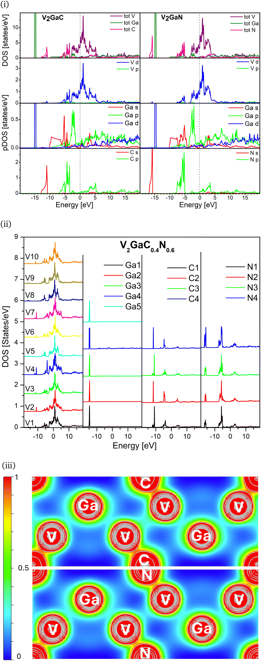 | ||
| Fig. 3 (i) Calculated density of states for V2GaC (on the left) and V2GaN (on the right). The top panel shows the total density of states, followed by the partial DOS of V, Ga, and C/N, which are color-coded. (ii) Represents calculated total DOS for nonequivalent atom sites present in (carbo)nitride phase V2GaC0.4N0.6. (iii) Calculated valence electron density of V2GaC (top) and V2GaN (bottom) in the (110) plane. This plane was selected to visualize the V, Ga, and C/N bonding scheme. The map is depicted by an isosurface of 0.827 with a minimum and maximum cutoff value of 0.018 and 0.998, respectively. | ||
Fig. 3ii shows the calculated total DOS for all nonequivalent atoms present in (carbo)nitride V2GaC0.4N0.6 unit cell. The structure is designed and optimized to represent the synthesized sample. The unit cell has ten vanadium, five gallium, and four nitrogen and carbon inequivalent sites, respectively. We find good agreement between our measurements and calculations. It is important to highlight that the calculated V2GaC0.4N0.6 structure replicates the combined DOS features of both V2GaC and V2GaN. The sites V2, V4 and V7 have the same peaks at −10.93 eV as V2GaC. Meanwhile sites V5, V8 and V9 have the same energy peak −16.15 eV as V2GaN. Additionally, sites V1, V3, V6 and V10 have energy features that are consistent with those observed in both V2GaN and V2GaC. The DOS for Ga, C, and N at all inequivalent sites is identical to that of the parent samples. This indicates that the electronic environment for Ga remains unaffected by the combined neighboring atoms, suggesting that the novel (carbo)nitride retains the electronic properties of both parent materials.
Now, the electron density color map in Fig. 3iii provides in-depth pictorial information to verify the novel bonding for Ga, V, C, and N in the systems. The maxima of the electron density of the Ga atoms are symmetric around the center, indicating that the electron density is confined to the atom. This confirms that the Ga interactions are the weakest with C/N and entirely metallic in both V2GaC and V2GaN structures. The almost spherical contours of the vanadium and carbon/nitrogen show a slight bending of contours towards each other in the system. The cyan color indicates the change in electron density between V and C/N atoms, suggesting that electron density is shared (light red) within the sample. This observation aligns with the expected covalent characteristics of the samples. However, conclusions driven by the color in the map for both samples reveal that the V–C bond exhibits a greater degree of covalency than the V–N bond, supporting the results obtained from our LFMT calculation. This is further supported by electron localization function45 (ELF) in Fig. 4 and Bader charge analysis46 in Table. S3 (ESI†).
 | ||
| Fig. 4 Electron localization function (ELF) maps for V2GaC (top) and V2GaN (bottom) MAX phases, illustrating the electron distribution and bonding nature in these layered ternary compounds. | ||
In Fig. 4, the ELF is visualized using a color contour plot ranging from blue to red (0 to 1). The delocalized electrons are projected in the lesser than 0.5. The regions shaded yellow-red correspond to high ELF values approaching 1.0, indicating strong electron localization, most notably around the Ga atoms. These observations are consistent with the Bader charge analysis presented in Table S3 (ESI†), which reveals significant charge transfer from vanadium to the carbon and nitrogen atoms, with net charges of +1.52 e and +1.48 e, respectively. This charge redistribution aligns with the high electronegativities of C and N. Notably, the ELF indicates a greater electron accumulation near the V–C bond compared to the V–N bond, suggesting stronger and more directional bonding in the former.
4. Conclusion
In this work, we explore the bonding and electronic properties of three vanadium-based MAX phases: V2GaC, V2GaN, and the (carbo)nitride phase V2GaC1−xNx. The parent models V2GaC and V2GaN exhibit distinct electronic features. V2GaC reveals a carbon vacancy in the structure, while V2GaN demonstrates significant splitting into t2g and eg bonding states. All the analysis indicates that there is no band gap in the samples, which reveals their metallic character. In the (carbo)nitride phase V2GaC1−xNx, we determine that the concentration of carbon and nitrogen are 40% and 60%, respectively with a chemical formula V2GaC0.4N0.6. These numbers validate the work by Kubitza et al.23 Also, we show that V2GaC0.4N0.6 retain the combined electronic properties as the parent samples. We examine the bonding mechanism in both V2GaC and V2GaN phases, emphasizing that the V2GaC has a higher degree of covalency than V2GaN. This is in contrast to typical electronegativity differences between carbon and nitrogen atoms.47 Among all atoms in the samples, V–Ga shows the weakest interaction with strong electron localization (metallic bonding) in both V2GaC and V2GaN. Furthermore, we established a formal oxidation state of V2.2+ for vanadium across all three MAX phases.Author contributions
Peter Ufondu: investigation, methodology, visualization, software, writing – original draft. Sakshi: investigation, methodology, visualization, writing – original draft. Teak D. Boyko: investigation, resources. Niels Kubitza: investigation, validation. Christina S. Birkel: project administration, validation. Alexander Moewes: project administration, supervision, validation and correction, funding acquisition.Conflicts of interest
There are no conflicts to declare.Data availability
The authors confirm that the data supporting the findings of this study are available within the article and its ESI.†Acknowledgements
This work is supported by the Natural Sciences and Engineering Research Council of Canada (NSERC), the Canada Research Chairs (CRC) program, the interdisciplinary Network for the Synchrotron: Promoting Innovation, Research, and Enrichment (NSERC CREATE) program, and the Deutsche Forschungsgemeinschaft (DFG, German Research Foundation) within CRC/TRR 270, project B03. All of the experimental research described in this paper was performed at the REIXS beamline of the Canadian Light Source, a national research facility of the University of Saskatchewan (USask), which is supported by the Canada Foundation for Innovation (CFI), the Natural Sciences and Engineering Research Council (NSERC), the Canadian Institutes of Health Research (CIHR), the Government of Saskatchewan, and the University of Saskatchewan. This research was enabled by computational support provided by the Digital Research Alliance of Canada (alliancecan.ca), and Plato (USask), which is managed by ICTs Advanced Research Computing (ARC) team.References
- M. W. Barsoum, Prog. Solid State Chem., 2000, 28, 201–281 CrossRef CAS.
- N. Kubitza, C. Büchner, J. Sinclair, R. M. Snyder and C. S. Birkel, ChemPlusChem, 2023, 88, e202300214 CrossRef CAS PubMed.
- M. A. Hadi, J. Phys. Chem. Solids, 2020, 138, 109275 CrossRef CAS.
- M. A. Hadi, J. Phys. Chem. C, 2023, 127, 23489–23503 CrossRef CAS.
- M. Li, J. Lu, K. Luo, Y. Li, K. Chang, K. Chen, J. Zhou, J. Rosen, L. Hultman, P. Eklund, P. O. Persson, S. Du, Z. Chai, Z. Huang and Q. Huang, J. Am. Chem. Soc., 2019, 141, 4730–4737 CrossRef CAS PubMed.
- H. Ding, Y. Li, M. Li, K. Chen, K. Liang, G. Chen, J. Lu, J. Palisaitis, P. O. Persson, P. Eklund, L. Hultman, S. Du, Z. Chai, Y. Gogotsi and Q. Huang, Science, 2023, 379, 1130–1135 CrossRef CAS PubMed.
- M. Dahlqvist, M. W. Barsoum and J. Rosen, Mater. Today, 2024, 72, 1–24 CrossRef.
- A. Bortolozo, O. SantAnna, C. dos Santos and A. Machado, Solid State Commun., 2007, 144, 419–421 CrossRef CAS.
- A. Bortolozo, G. Serrano, A. Serquis, D. Rodrigues, C. dos Santos, Z. Fisk and A. Machado, Solid State Commun., 2010, 150, 1364–1366 CrossRef CAS.
- J. P. Siebert, S. Mallett, M. Juelsholt, H. Pazniak, U. Wiedwald, K. Page and C. S. Birkel, Mater. Chem. Front., 2021, 5, 6082–6091 RSC.
- C. M. Hamm, J. D. Bocarsly, G. Seward, U. I. Kramm and C. S. Birkel, J. Mater. Chem. C, 2017, 5, 5700–5708 RSC.
- M. Naguib, O. Mashtalir, J. Carle, V. Presser, J. Lu, L. Hultman, Y. Gogotsi and M. Barsoum, ACS Nano, 2012, 6, 1322–1331 CrossRef CAS PubMed.
- M. Naguib, M. W. Barsoum and Y. Gogotsi, Adv. Mater., 2021, 33, 2103393 CrossRef CAS PubMed.
- W. Jeitschko, H. Nowotny and F. Benesovsky, Monatsh. Chem., 1964, 95, 178–179 CrossRef CAS.
- W. Jeitschko, H. Nowotny and F. Benesovsky, Monatsh. Chem., 1964, 95, 156–157 CrossRef CAS.
- O. Beckmann, H. Boller, H. Nowotny and F. Benesovsky, Monatsh. Chem., 1969, 100, 1465–1470 CrossRef CAS.
- A. Greenaway, C. Melamed, M. Tellekamp, R. Woods-Robinson, E. Toberer, J. Neilson and A. Tamboli, Annu. Rev. Mater. Res., 2021, 51, 591–618 CrossRef CAS.
- W. Yu, V. Mauchamp, T. Cabioch, D. Magne, L. Gence, L. Piraux, V. Gauthier-Brunet and S. Dubois, Acta Mater., 2014, 80, 421–434 CrossRef CAS.
- T. Cabioch, P. Eklund, V. Mauchamp and M. Jaouen, J. Am. Ceram. Soc., 2012, 32, 1803–1811 CAS.
- M. A. Pietzka and J. C. Schuster, J. Am. Ceram. Soc., 1996, 79, 2321–2330 CrossRef CAS.
- N. Kubitza, I. Huck, H. Pazniak, C. Kalha, D. Koch, B. Zhao, P. K. Thakur, T.-L. Lee, A. A. Riaz, W. Donner, H. Zhang, B. Moss, U. Wiedwald, A. Regoutz and C. S. Birkel, J. Mater. Chem. C, 2024, 12, 7552–7561 RSC.
- N. Kubitza, B. Beckmann, S. Jankovic, K. Skokov, A. A. Riaz, C. Schlueter, A. Regoutz, O. Gutfleisch and C. S. Birkel, Chem. Mater., 2024, 36, 1375–1384 CrossRef CAS.
- N. Kubitza, A. Reitz, A.-M. Zieschang, H. Pazniak, B. Albert, C. Kalha, C. Schlueter, A. Regoutz, U. Wiedwald and C. S. Birkel, Inorg. Chem., 2022, 61, 10634–10641 CrossRef CAS PubMed.
- Z. Du, C. Wu, Y. Chen, Q. Zhu, Y. Cui, H. Wang, Y. Zhang, X. Chen, J. Shang, B. Li, W. Chen, C. Liu and S. Yang, Adv. Energy Mater., 2022, 12, 2103228 CrossRef CAS.
- M. Magnuson and M. Mattesini, Thin Solid Films, 2017, 621, 108–130 CrossRef CAS.
- P. Ufondu, T. D. Boyko, M. M. Pointner, L. Eisenburger, W. Schnick and A. Moewes, J. Mater. Chem. C, 2024, 12, 4392–4398 RSC.
- P. Ufondu, Sakshi, T. D. Boyko, M. M. Pointner, W. Schnick and A. Moewes, Adv. Sci., 2025, 12, 2412830 CrossRef CAS PubMed.
- K. Schwarz, P. Blaha and G. Madsen, Comput. Phys. Commun., 2002, 147, 71–76 CrossRef.
- P. Blaha, K. Schwarz, G. Madsen, D. Kvasnicka, J. Luitz, R. Laskowski, F. Tran and L. Marks, Tech. Univer. Wien, 2018, 3–9501031 Search PubMed.
- J. P. Perdew, K. Burke and M. Ernzerhof, Phys. Rev. Lett., 1996, 77, 3865–3868 CrossRef CAS PubMed.
- P. Blaha, K. Schwarz, F. Tran, R. Laskowski, G. Madsen and L. Marks, J. Chem. Phys., 2020, 152, 0021–9606 CrossRef PubMed.
- M. W. Haverkort, M. Zwierzycki and O. K. Andersen, Phys. Rev. B: Condens. Matter Mater. Phys., 2012, 85, 165113 CrossRef.
- Y. Lu, M. Höppner, O. Gunnarsson and M. W. Haverkort, Phys. Rev. B: Condens. Matter Mater. Phys., 2014, 90, 085102 CrossRef.
- M. W. Haverkort, G. Sangiovanni, P. Hansmann, A. Toschi, Y. Lu and S. Macke, EPL, 2014, 108, 57004 CrossRef.
- M. W. Haverkort, J. Phys.:Conf. Ser., 2016, 712, 012001 CrossRef.
- M. J. D. Powell, Comput. J., 1964, 7, 155–162 CrossRef.
- T. M. Tolhurst, B. Leedahl, J. L. Andrews, P. M. Marley, S. Banerjee and A. Moewes, Phys. Chem. Chem. Phys., 2016, 18, 15798–15806 RSC.
- D. Maganas, M. Roemelt, T. Weyhermüller, R. Blume, M. Hävecker, A. Knop-Gericke, S. DeBeer, R. Schlögl and F. Neese, Phys. Chem. Chem. Phys., 2014, 16, 264–276 RSC.
- R. Kapoor, S. T. Oyama, B. Friihberger, B. D. DeVries and J. G. Chen, Catal. Lett., 1995, 34, 179–189 CrossRef CAS.
- G. Abrasonis, M. Berndt, M. Krause, K. Kuepper, F. Munnik, A. Kolitsch and W. Möller, J. Phys. Chem. C, 2008, 112, 17161–17170 CrossRef CAS.
- J. Stöhr, NEXAFS Spectroscopy, Springer, 1992 Search PubMed.
- J. Etzkorn, M. Ade and H. Hillebrecht, Inorg. Chem., 2007, 46, 7646–7653 CrossRef CAS PubMed.
- M. Krbal, A. Kolobov, P. Fons, K. Mitrofanov, Y. Tamenori, B. Hyot, B. Andre and J. Tominaga, J. Alloys Compd., 2017, 704, 254–259 CrossRef CAS.
- A. Bouhemadou, Solid State Sci., 2009, 11, 1875–1881 CrossRef CAS.
- P. Giannozzi, S. Baroni, N. Bonini, M. Calandra, R. Car, C. Cavazzon, D. Ceresoli, G. L. Chiarotti, M. Cococcioni, I. Dabo and A. Dal Corso, et al., J. Phys. Condens. Matter, 2009, 21, 395–502 CrossRef PubMed.
- W. Tang, E. Sanville and G. Henkelman, J. Phys. Condens. Matter, 2009, 21, 084–204 Search PubMed.
- M. Magnuson, MRS Proc., 2007, 1023, 901 Search PubMed.
Footnote |
| † Electronic supplementary information (ESI) available. See DOI: https://doi.org/10.1039/d5ma00222b |
| This journal is © The Royal Society of Chemistry 2025 |