
 Open Access Article
 This Open Access Article is licensed under a Creative Commons Attribution-Non Commercial 3.0 Unported Licence
Strongly coupled C@SiOx/MoSe2@NMWCNT heterostructures as anodes for Na+ batteries with excellent stability and capacity†
Mengru
Bian‡
 a,
Yincai
Yang‡
a,
Youwen
Chen
*ab,
Tiantian
Wei
a,
Wei
Deng
*a,
Biao
Fu
a and
Renhua
Qiu
*a
a,
Yincai
Yang‡
a,
Youwen
Chen
*ab,
Tiantian
Wei
a,
Wei
Deng
*a,
Biao
Fu
a and
Renhua
Qiu
*a
aCollege of Chemistry and Chemical Engineering, Hunan University, Changsha, 410081, China. E-mail: 36928664@qq.com; renhuaqiu1@hnu.edu.cn
bSchool of Information and Mechanical Engineering, Hunan International Economics University, Changsha, 410205, China
First published on 20th March 2025
Abstract
Silicon and silicon oxide have become the most prospective anode materials, but the volume variations during charging and discharging have greatly hindered their practical applications. Herein, we constructed a highly ordered, dispersed silicon-molybdenum composite, C@SiOx/MoSe2@NMWCNT, with a three-layer heterojunction structure. In this approach, molybdenum pentachloride (MoCl5) reacts with ethylene glycol to form an ethylene glycol-based organomolybdenum complex, which then undergoes a reaction with triphenylchlorosilane, effectively bridging silicon and molybdenum to form an organometallic compound. After in situ selenization and carbonization, the formed SiOx is dispersed in the framework of MoSe2 nanoflaps to form a SiOx/MoSe2 composite structure. It is then adsorbed onto carbon nanotubes (NMWCNTs) with nitrogen-containing active sites, forming a three-layer heterojunction structure with the outer carbon layer. When used as a sodium-ion battery (SIB) anode, C@SiOx/MoSe2@NMWCNT exhibits an initial discharge-specific capacity (1315 mA h g−1 at 0.1 A g−1) and a high capacity of 526 mA h g−1 after 300 cycles at 0.5 A g−1, demonstrating excellent long-cycle stability. When the current density reaches 5 A g−1, the specific capacity remains at 415 mA h g−1 after 1000 cycles and 353 mA h g−1 after 3000 cycles. Even under a high current density of 10 A g−1, the material maintains remarkable cycling stability, delivering a capacity of 177.79 mA h g−1 after 3000 cycles, illustrating the high potential of silicon for use in SIBs.
Introduction
Nowadays,1,2 lithium-ion batteries (LIBs) are largely used for mobile electronics and electric-powered vehicles due to their excellent energy density.3,4 However, owing to the relatively small spatial arrangement of lithium occurrences, it is necessary to explore alternatives for LIBs. SIBs are gaining traction owing to abundant availability and mechanisms analogous to those of LIBs.5–8 Since Na+ has a larger radius (1.06 Å)9 compared to Li+ (0.76 Å), the insertion and extraction kinetics of Na+ are slower than those of Li+.10 Thus, it is imperative to develop suitable anode materials for SIBs.Silicon, which is abundant on Earth, has a theoretical specific capacity of approximately 4200 mA h g−1,11 ten times that of conventional carbon anodes.12 Coupled with their environmental friendliness, natural abundance, and low cost,13 silicon-based materials (e.g., Si, SiOx) are regarded as promising anode materials for LIBs.14–16 Researchers have developed several strategies to enhance the functionality of LIBs, such as nanomaterials,17,18 structural engineering,19–21 and composite materials.22–24 Cao et al. created a Cu–Si nanoarray targeted at boosting the efficiency of LIBs,25 Ma et al. successfully designed a conductive 3D porous silicon structure26 to address the volume expansion problem caused by silicon during lithiation and delithiumization, and Zhong et al. invented a hollow Co/N-C@SiO2 composite to optimize SiO2 conductivity in LIBs.27 However, most of these silicon materials used for LIBs are unsuitable for SIBs because Na+, with its larger radius, creates a relatively high diffusion barrier for sodium ions. Additionally, the larger volume expansion of silicon reduces battery performance.28–30 To address these issues, methods such as designing nanostructured silicon, incorporating silicon into buffer matrices, designing silicon composite structures with conductive carbon materials, and doping of metallic elements have been recommended. Yao et al. successfully created Si/TiO2−x@C anode materials with porous structure for sodium-ion batteries by introducing Si into TiO2−x@C MOF structure acting as buffer layers, this MOF structure enhances the stability of the electrode in cycling operations, but Si does not exhibit its own high capacity due to the low conductivity of TiO2 (190 mA h g−1@2 A g−1, 2500 cycles).28 Ma et al. invented a new type of double-layer protective material Si@MnSe@PPyC/rGO for relieving volume changes for sodium-ion batteries, where nanopetaloidal MnSe serves as a buffer matrix wrapped around larger silicon particles and grows on the highly conductive PPyC/rGO carbon material, which can reduce the volume expansion of Si, but aggregation of silicon particles may occur during cycling, preventing silicon from consistently exhibiting a high capacity (226.4 mA h g−1@2 A g−1, 500 cycles).31 Hirono et al. inserted conductive Sn into SiOx to form Sn/SiOx for improving sodium-ion batteries conductivity; although the electrical conductivity improved, the volume expansion of silicon led to poor cycling stability (340 mA h g−1@0.05 A g−1, 100 cycles).32 Researchers have done a lot of work, but the results are still unsatisfactory,33 as the issues of large volume expansion of silicon and the high diffusion energy barrier of Na+ due to its larger radius have not been simultaneously addressed.
With the above challenge in mind, we designed to address these issues by uniformly dispersing SiOx on MoSe2 nanosheets to form a SiOx/MoSe2 composite structure. As we know, the layered molybdenum-based compounds have been disclosed as natural channels for the diffusion of Na+,34 especially MoSe2, the interlayer distance of 0.66 nm is greater than that of which is 0.62 nm.35–37 Therefore, MoSe2 can suppress the aggregation of SiOx particles to improve dispersion, act as a stabilizing layer to reduce volume variations, and provide diffusion channels for sodium ions by reducing the energy barrier of sodium ions. For composite preparation, carbon nanotubes (CNTs) with unique flexibility,38,39 high chemical stability and electrical conductivity are usually used as a template,40 which not only allows the electrolyte to penetrate widely to improve its electronic and ionic conductivity but also adapts to volume changes in composites. In addition, by introducing functional groups featuring nitrogen (like pyridine-N, pyrrole-N, graphite-N, and pyridine-oxide-N) as active sites on CNTs,41–43 SiOx/MoSe2 can be further adsorbed on the active sites of nitrogen (N)-doped carbon nanotubes (NMWCNT) to form a three-layered heterojunction structure, which may prevent detachment from the electrode and enhance conductivity.
In this study, we constructed a highly ordered, dispersed silicon-molybdenum composite of C@SiOx/MoSe2@NMWCNT with a three-layer heterojunction structure. The outermost carbon layer obtained by carbonizing organic matter and NMWCNT forms a protective interlayer in which SiOx/MoSe2 grows. It not only prevents the buildup of a thick SEI film but also mitigates volume expansion caused by the entry and extraction of Na+. This method not only enhances the capacity of batteries (526 mA h g−1@0.5 mA g−1, 300 cycles) but also improves their cycling stability for SIBs (415 mA h g−1, 353 mA h g−1@5 A g−1, 1000 cycles and 3000 cycles). Therefore, the C@SiOx/MoSe2@NMWCNT composite, with its three-layer heterostructure, shows great promise as an anode material for SIBs due to its synergistic advantages: the carbon layer ensures structural stability and conductivity, the SiOx provides high capacity and cycling stability, and the MoSe2 layer facilitates efficient sodium-ion diffusion. Combined with the mechanical strength and enhanced conductivity of NMWCNTs, this composite addresses key challenges such as volume expansion and low conductivity, making it a strong candidate for high-performance SIB applications.
Results and discussion
As illustrated in Fig. 1, we reacted molybdenum pentachloride (MoCl5) with ethylene glycol to form an ethylene glycol-based organomolybdenum complex via ultrasonic treatment, followed by a reaction with triphenylchlorosilane via further ultrasonic treatment, which effectively bridges silicon and molybdenum to form an organometallic compound. This indicates that Mo–Si organometallic compounds were formed successfully in high-resolution mass spectra (Fig. S1–S4†). Then, after in situ selenization and carbonization at 800 °C, the anode material C@SiOx/MoSe2@NMWCNT was successfully obtained. Within the same method, we successfully prepared C@MoSe2, C@SiOx@NMWCNT and C@SiOx/MoSe2@C composites through ultrasound and calcination (see Experimental section). | ||
| Fig. 1 Preparation process of C@SiOx/MoSe2@NMWCNT, (a) MoCl5 mixed with ethylene glycol to form organomolybdenum complexes by ultrasonic treatment; (b) organomolybdenum complexes mixed with ph3SiCl and ethylene glycol to form Si/Mo-organometallic by ultrasonic treatment; (c) Si/Mo-organometallic mixed with NMWCNT to form Si/Mo-organometallic@NMWCNT by ultrasonic treatment; (d) composite C@SiOx/MoSe2@NMWCNT obtained by in situ selenization at 800 °C; (e) C@SiOx/MoSe2@NMWCNT with three-layer structure; (f) TEM image of C@SiOx/MoSe2@NMWCNT. | ||
The structures of C@MoSe2, C@SiOx@NMWCNT, C@SiOx/MoSe2@C, and C@SiOx/MoSe2@NMWCNT were characterized using SEM and TEM. In previous studies,44 we can see that C@MoSe2 has a sheet-like structure and is intertwined with each other to create a 3D flower-like structure. The MoSe2 nanosheets were verified to be coated with a carbon layer. Fig. S5 and S6† show that the carbon-coated SiOx grows on NMWCNTs to form a three-layer heterojunction composite C@SiOx@NMWCNT, and the adsorption of C@SiOx has almost no effect on the morphology of the NMWCNTs. From the EDS element analysis in Fig. S6(d–g),† we can see four elements: C, Si, O, and N, where the Si and O elements gather to confirm the formation of SiOx and also provide an idea for the subsequent addition of MoSe2 to act as a skeleton for dispersing SiOx.
As shown in Fig. S7 and S8,† many MoSe2 nanosheets are formed in C@SiOx/MoSe2@C materials, and the formation of SiOx and MoSe2 can be seen according to the TEM electron image and EDS element analysis in Fig. S8(c–i),† and the homogeneous dispersion of Mo, Se, C, O, and Si elements also indicates that SiOx is uniformly dispersed on the MoSe2 nanosheets, and the organic components acted as carbon sources to form a carbon coating.
Fig. 2 shows the SEM image of C@SiOx/MoSe2@NMWCNT, in which (a–c) SiOx/MoSe2 = 2![[thin space (1/6-em)]](https://www.rsc.org/images/entities/char_2009.gif) :1, (d–f) SiOx/MoSe2 = 3:1, (g–i) SiOx/MoSe2 = 4:1 and (j–l) SiOx/MoSe2 = 5:1. Comparing the above four sets of plots, with the increase in the SiOx ratio, the morphology of the NMWCNT changes a little. As shown in Fig. 2(g–l), the surface of the NMWCNTs is somewhat deformed, and the pipe walls become very thick, which hinders the transport of sodium ions and decreases their mobility. Compared with Fig. 2(g–l), the carbon nanotube skeletons in Fig. 2(a–f) are almost not affected, especially in Fig. 2(d–f), some MoSe2 nanosheets can be seen growing on the NMWCNT like fish scales, and some like leaves, which can boost the contact area for the active substance and electrolyte while also offering an improved channel for sodium ions to enter. Sodium-ion mobility and active material utilization efficiency are enhanced. Therefore, we selected SiOx/MoSe2 = 3:1 as the best ratio.
:1, (d–f) SiOx/MoSe2 = 3:1, (g–i) SiOx/MoSe2 = 4:1 and (j–l) SiOx/MoSe2 = 5:1. Comparing the above four sets of plots, with the increase in the SiOx ratio, the morphology of the NMWCNT changes a little. As shown in Fig. 2(g–l), the surface of the NMWCNTs is somewhat deformed, and the pipe walls become very thick, which hinders the transport of sodium ions and decreases their mobility. Compared with Fig. 2(g–l), the carbon nanotube skeletons in Fig. 2(a–f) are almost not affected, especially in Fig. 2(d–f), some MoSe2 nanosheets can be seen growing on the NMWCNT like fish scales, and some like leaves, which can boost the contact area for the active substance and electrolyte while also offering an improved channel for sodium ions to enter. Sodium-ion mobility and active material utilization efficiency are enhanced. Therefore, we selected SiOx/MoSe2 = 3:1 as the best ratio.
 | ||
| Fig. 2 SEM images of (a–c) C@SiOx/MoSe2–2:1@NMWCNT, (d–f) C@SiOx/MoSe2–3:1@NMWCNT, (g–i) C@SiOx/MoSe2–4:1@NMWCNT and (j–l) C@SiOx/MoSe2–5:1@NMWCNT. | ||
The HAADF-STEM images of C@SiOx/MoSe2–3:1@NMWCNT can also be seen that the leaf-like MoSe2 nanosheets are grown at an angle on the NMWCNT (Fig. 3b), and the EDS element analysis of Fig. 3(e–l) indicates the uniform distribution of elements (C, N, O, Si, Se, Mo), which also shows that SiOx particles are evenly dispersed on MoSe2 nanosheets, which provides a high-capacity potential for the composite during charging and discharging. The lattice layer spacing in both HR-TEM Fig. 3c and d is approximately 0.65 nm, which matches the (002) plane of MoSe2, which also proves that a large number of MoSe2 nanosheets have been formed, which offers a good channel for the embedding of Na+, probably improves the storage capacity of sodium ions, and also plays a role in dispersing and storing silicon, upgrading the battery's capabilities.
 | ||
| Fig. 3 (a and b) TEM images of C@SiOx/MoSe2–3:1@NMWCNT, (c and d) HRTEM images of C@SiOx/MoSe2–3:1@NMWCNT, (e) STEM images of C@SiOx/MoSe2–3:1@NMWCNT, (f) elemental distribution of C@SiOx/MoSe2–3:1@NMWCNT and corresponding (g)–(l) EDS-mapping element maps. | ||
To further authenticate the properties of the synthetic materials, XRD, Raman, and XPS analyses were conducted. Fig. 4a shows the XRD images of C@MoSe2, C@SiOx/MoSe2@C and C@SiOx/MoSe2–3:1@NMWCNT from 10 to 80 (2θ). The peaks at 26.2° for C@SiOx/MoSe2@C and C@SiOx/MoSe2–3:1@NMWCNT correspond to the (011) plane of SiO2 (JCPDS 47-1144), and the peaks at 47° and 56° correspond to SiO (JCPDS 30-1127). With the exception of these peaks, the other peaks correspond to the MoSe2 (JCPDS 29-0914) peak group, indicating the significant formation of MoSe2. Fig. 4b, S9a† and 4c show the Raman spectra for C@MoSe2, NMWCNT, C@SiOx/MoSe2@C, and C@SiOx/MoSe2–3:1@NMWCNT, as shown in Fig. 4b, where 238.0 cm−1 represents the out-of-plane atomic vibration mode (A1g) of MoSe, and 283.1 cm−1 represents the in-plane atomic vibration mode (E12g) of MoSe. The strength ratios of C@MoSe2 (12.29), C@SiOx/MoSe2@C (1.08) and C@SiOx/MoSe2–3:1@NMWCNT (1.19) from A1g to E12g are quite different, indicating that SiOx has a certain influence on the layered structure of MoSe2, and confirms that SiOx is successfully inserted and attached to the layered structure of MoSe2 to form SiOx/MoSe2 composites. The results also suggest a powerful interaction between NMWCNTs and SiOx/MoSe2. In Fig. 4c, the Raman images for C@MoSe2, NMWCNT, C@SiOx/MoSe2@C and C@SiOx/MoSe2–3:1@NMWCNT show that the two peaks at 1352 cm−1 and 1586 cm−1 are the D and G segments of NMWCNT,37 and the D/G respectively matches to C@MoSe2 (0.91), NMWCNT (1.0), C@SiOx/MoSe2@C (0.96) and C@SiOx/MoSe2–3:1@NMWCNT (0.92). The strength ratios are almost identical, proving that they have similar degrees of defect.38
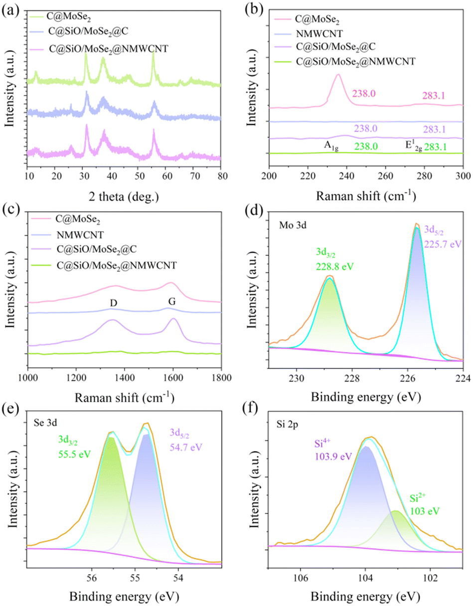 | ||
| Fig. 4 (a) XRD patterns of C@MoSe2, C@SiOx/MoSe2@C, C@SiOx/MoSe2–3:1@NMWCNT, (b and c) Raman spectra of C@MoSe2, NMWCNT, C@SiOx/MoSe2@C, C@SiOx/MoSe2–3:1@NMWCNT, and high-resolution XPS (d) Mo 3d spectrum, (e) Se 3d spectrum, (f) Si 2p spectrum of C@SiOx/MoSe2–3:1@NMWCNT. | ||
XPS was used to analyze the elemental composition and oxidation states at the surface of the C@SiOx/MoSe2–3:1@NMWCNT composites. The O, Mo, N, C, Se and Si signals can be observed in the full spectrum (Fig. S9b†). In the Mo 3d spectrum (Fig. 4d), the Mo 3d3/2 signal is observed at 228.8 eV, and the Mo 3d5/2 signal is observed at 225.7 eV, indicating the state of Mo4+. In Fig. 4e (Se 3d spectrum), the Se 3d3/2 signal is observed at 55.5 eV, and the Se 3d5/2 signal is observed at 54.7 eV, indicating the state of Se2+. In the Si 2p spectrum (Fig. 4f), the signals at 103.9 eV and 103 eV correspond to tetravalent and divalent silicon, respectively, confirming the formation of SiO2 and SiO. In Fig. S9d† (N 1s spectrum), there are three main peaks, which are 401.1 eV, 399.3 eV, and 395.1 eV, matching graphitic-N, pyrrolic-N and pyridinic-N.45 In Fig. S9c† (C 1s spectrum), there are four main peaks at 288.8 eV, 286.8 eV, 285.6 eV and 284.8 eV, respectively named C![[double bond, length as m-dash]](https://www.rsc.org/images/entities/char_e001.gif) O, C–O, C–N and C–C bonds.
O, C–O, C–N and C–C bonds.
The MoSe2 and SiOx contents in C@MoSe2, C@MoSe2@NMWCNT and C@SiOx/MoSe2 (2/3/4:1) @NMWCNT were determined by thermogravimetric analysis (TGA) (Fig. S10†). When heated in air, SiOx is completely converted to SiO2, and its weight changes negligibly, and MoSe2 oxidizes to form MoO3 and SeO2 before 350 °C; therefore, there is a phenomenon of weight increase. Thereafter, there will be two phases of weight loss. The first stage of weight reduction is due to SeO2 sublimation, and the second stage of weight reduction is due to carbon oxidation. At temperatures of 900–1000 °C, the residues of C@MoSe2 and C@MoSe2@NMWCNT were only 2.2% and 3.5%. The products of C@MoSe2 and C@MoSe2@NMWCNT calcined at 900 °C for 4 h were detected by SEM (Fig. S11†) and TEM (Fig. S12 and S13†), and the results indicated that the product was predominantly MoO3 encapsulated within the C–O–Mo frame (MoO3 accounted for 99.47% of the product composition in Fig. S12e†).
Combined with the conservation principle applied to the Mo element, the proportion of MoSe2 can be calculated using eqn (1).
 | (1) |
:1@NMWCNT, C@SiOx/MoSe2–3:1@NMWCNT, and C@SiOx/MoSe2–4:1@NMWCNT are 53.1%, 30.4%, 30.9%, 25.2%, and 23.9%, respectively. The MoSe2 contents in C@MoSe2, C@MoSe2@NMWCNT, C@SiOx/MoSe2–2:1@NMWCNT, C@SiOx/MoSe2–3:1@NMWCNT and C@SiOx/MoSe2–4:1@NMWCNT were calculated to be 93.6%, 53.6%, 54.5%, 44.4% and 42.2%, respectively. The SiOx contents in C@SiOx/MoSe2–2:1@NMWCNT, C@SiOx/MoSe2–3:1@NMWCNT, and C@SiOx/MoSe2–4:1@NMWCNT were 2.5%, 14%, and 19.2%, respectively.
Next, we tested the energy storage performance of the SIBs of four materials (Fig. 5): C@MoSe2, C@SiOx@NMWCNT, C@SiOx/MoSe2@C, and C@SiOx/MoSe2–3:1@NMWCNT by making button batteries. Fig. 5a shows the cyclic voltammetry (CV) curve of the C@SiOx/MoSe2–3:1@NMWCNT composite as an SIB electrode. In the initial cyclic voltammetry (CV) scan, three cathodic peaks were noted at 1.03 V, 0.63 V, and 0.36 V. The peak (1.03 V) represents the process by which Na+ is inserted into MoSe2 to form NaxMoSe2, and then NaxMoSe2 is converted to Mo and Na2Se. The peaks (0.63 V, 0.36 V) respectively stand for the alloying of amorphous Si and the development of a solid electrolyte interface (SEI) layer.46 These two peaks vanished during the second cycle, resulting in an initial irreversible high capacity. Furthermore, during the charging process, two anodic peaks appeared at 1.73 V and 2.0 V. The peak (1.73 V) represents the process in which Mo is partially oxidized to MoSe2 and Na2Se is partially converted to Se. Meanwhile, the peak (2.0 V) is due to the dealloying of Si.
 | ||
| Fig. 5 (a) CV curves at a scan rate of 0.1 mV s−1, (b) galvanostatic discharge and charge voltage curves (0.1 A g−1) of C@SiOx/MoSe2–3:1@NMWCNT, (c) discharge and charge profiles (0.5 A g−1) of C@SiOx/MoSe2–1/2/3/4/5:1@NMWCNT, (d) rate capacity of C@SiOx/MoSe2–3:1@NMWCNT, (e) long-term tests (5 A g−1, 10 A g−1) of C@SiOx/MoSe2–3:1@NMWCNT. | ||
From the ex situ TEM images of C@SiOx/MoSe2–3:1@NMWCNT (Fig. S14a, b and S15b†), When charged to either 3 V or 2 V, the spacing between lattice layers, matching the (004) plane of MoSe2, measured approximately 0.33 nm. Additionally, the concentration of Se (Fig. S14j†) further confirmed the presence of Se. From the second cycle, the main cathodic peak at 1.38 V is a result of further insertion of Na+. In addition, from the second cycle onwards, the cyclic voltammetry (CV) curve remains nearly overlapping, signifying the material's stability when charged and discharged. Fig. 5b shows the galvanostatic charge and discharge profiles (at 0.1 A g−1) of the material C@SiOx/MoSe2–3:1@NMWCNT as an SIB electrode. The first discharge and charge capacities were 1178 and 649 mA h g−1, respectively, with a charge/discharge efficiency of 55% in the first cycle. The low efficiency of the initial charge–discharge process can be attributed to the formation of an SEI layer during the first cycle. The charge/discharge efficiency rapidly increased to 88.7% in the second cycle and continued to exceed 95% in subsequent cycles, indicating the excellent reversibility of the C@SiOx/MoSe2–3:1@NMWCNT anode.
Fig. 5c shows the charge–discharge ratio capacity and cycle durability of the material C@SiOx/MoSe2@NMWCNT at 1:1, 2:1, 3:1, 4:1, and 5:1 for SiOx/MoSe2 (at 0.5 A g−1, and the initial five cycles at 0.1 A g−1), and it is observable that the charge/discharge capacity is lower at 1:1, 2:1, 4:1, and 5:1 for SiOx/MoSe2. At 3:1 for SiOx/MoSe2, superior charge–discharge capacity and enhanced cycle stability were achieved, with the discharge capacity remaining at 526 mA h g−1 even after 300 cycles.
As depicted in Fig. S16,† the sodium-ion battery (SIB) electrode demonstrates significant capacitance attenuation and poor cycling stability without SiOx or NMWCNT participation. For C@MoSe2, after 300 cycles (at 0.1 A g−1), the discharge capacity decreases to 99 mA h g−1. For C@SiOx@NMWCNT, the incorporation of silicon leads to a growth in the initial capacity when charged and discharged. However, after five cycles, the specific capacity for charging and discharging began to decline, and over 300 cycles (at 0.5 A g−1), the average discharge capacity is approximately 225 mA h g−1. For C@SiOx/MoSe2@C, after 300 cycles (at 0.5 A g−1), the discharge-specific capacity drops to 378 mA h g−1, indicating poor cycling stability. These results indicate that the three-layer C@SiOx/MoSe2–3:1@NMWCNT heterojunction material exhibits an elevated specific capacity for charging and discharging and good cycle stability. Among them, SiOx and MoSe2 exhibit the best battery performance when added at a ratio of 3:1 (C@SiOx/MoSe2–3:1@NMWCNT). Their TEM, SEM and thermogravimetric analyses revealed that SiOx/MoSe2 had more exposed edges and concentrations, providing more active sites when C@SiOx/MoSe2 was grown on NMWCNT, thereby enhancing the specific capacity and stability over multiple cycles.
Fig. 5d illustrates the rate performance of the C@SiOx/MoSe2–3:1@NMWCNT, where a gradual decline in specific capacity is observed when the current density escalates from 0.1 to 10 A g−1. When the current densities were 0.1, 0.2, 0.4, 0.8, 1.0, 1.5, 2.0, 3.0, 4.0, 5.0 and 10.0 A g−1, respectively, the respective discharge-specific capacities were 720, 644, 588, 536, 516, 485, 464, 434, 410, 395 and 347 mA h g−1. Upon reverting the current density to 0.1 A g−1, the discharge capacity recovers to 660 mA h g−1, indicating favorable reversibility. Fig. 5e highlights the exceptional durability of the C@SiOx/MoSe2–3:1@NMWCNT, exhibiting a remarkable capacity retention of 353 mA h g−1 after 3000 cycles at a current density of 5 A g−1. Even at a higher current density of 10 A g−1, it demonstrated excellent cycling stability, retaining 177.79 mA h g−1 after 3000 cycles. Compared with C@MoSe2, C@SiOx@NMWCNT, and C@SiOx/MoSe2@C, the C@SiOx/MoSe2–3:1@NMWCNT composites combine high-capacity SiOx with MoSe2 to form SiOx/MoSe2, which is grown on NMWCNT to provide additional active locations for storing Na+ and improve the capacity as SIB electrodes. Simultaneously, the application of a carbon layer mitigates the volume fluctuations of the composite material when charged and discharged, thereby enhancing its cyclic stability.
The SEM images (Fig. 6a and b) show the change in the electrode sheet thickness of the C@SiOx/MoSe2–3:1@NMWCNT composite as the SIB electrode before and after charging and discharging. The results show that the morphology of C@SiOx/MoSe2–3:1@NMWCNT remained stable after charging and discharging, the electrode sheet thickness increased from 17.8 μm to 20.9 μm on average, and the structure did not collapse significantly. This proves that the unique three-layer heterojunction structure of the C@SiOx/MoSe2–3:1@NMWCNT composites buffers the volume changes when charged and discharged, thereby boosting the stability of the C@SiOx/MoSe2–3:1@NMWCNT composites and their durable cycling performance as SIB electrode materials.
 | ||
| Fig. 6
In situ SEM thickness analysis images of C@SiOx/MoSe2–3:1@NMWCNT: (a) charge from open-circuit voltage 0.01 V to 3 V, (b) discharge from open-circuit voltage 3 V to 0.01 V. | ||
The modifications made to silicon used as an anode material for SIBs are presented in Table 1. These include carbon coating, elemental doping, porous structure and composite material preparation. Although the volume expansion problem of silicon has been solved somewhat, the capacity is still not only satisfactory, so we try to synthesize the composite C@SiOx/MoSe2@NMWCNT by adding high-capacity SiOx into MoSe2, which has a two-dimensional structure, so that the lamellar structure of MoSe2 relieves the volume expansion brought by SiOx along with mutually improving the overall capacity, and NMWCNT can also provide good electrical conductivity. Compared to their work, our three-layer C@SiOx/MoSe2@NMWCNT composite exhibits not only superior structural stability but also higher capacity. This enhancement was attributed to the excellent dispersion of SiOx facilitated by the layered MoSe2 nanosheets. These nanosheets provide abundant active sites, ensuring the uniform dispersion of high-capacity SiOx and preventing its aggregation during cycling. Therefore, when the C@SiOx/MoSe2@NMWCNT with a three-layer heterojunction structure is used for the anode of SIBs, it exhibits excellent charging and discharging performance with high discharge capacity and good stability performance.
| Anode material | Synthesis method | Rate performance | Long-cycle performance | Ref. |
|---|---|---|---|---|
| SiOx/C | Annealing | 530 mA h g−1@0.03 A g−1, 300 mA h g−1@0.1 A g−1 | 200 mA h g−1@0.3 A g−1, 100 cycles | 47 |
| Sn/SiOx | Jet milling | 340 mA h g−1@0.05 A g−1, 100 cycles | 32 | |
| 2D Si-Ge | Ball milling, annealing | 540 mA h g−1@0.05 A g−1, 130 mA h g−1@2 A g−1 | 276 mA h g−1@0.05 A g−1, 50 cycles | 48 |
| Si/TiO2−x@C | Annealing | 365.4 mA h g−1@0.1 A g−1, 233.3 mA h g−1@2 A g−1 | 191 mA h g−1@2 A g−1, 2500 cycles | 28 |
| Si@MnSe@PPyC/rGO | Chemical bath deposition, freeze-drying | 313 mA h g−1@0.1 A g−1, 226.4 mA h g−1@2 A g−1 | 323 mA h g−1@0.2 A g−1, 270 cycles | 31 |
| C@SiOx/MoSe2@NMWCNT | Annealing | 720 mA h g−1@0.1 A g−1, 347 mA h g−1@10 A g−1 | 415 mA h g−1@5 A g−1, 1000 cycles, 353 mA h g−1@5 A g−1, 3000 cycles | This work |
The capacitance contribution of the C@SiOx/MoSe2–3:1@NMWCNT composites was studied based on their CV data, and Fig. 7a shows the CV curves of the C@SiOx/MoSe2–3:1@NMWCNT over a range of 0.2–1.2 mV s−1 scan velocity. The b value at the anode (cathode) peak can be determined based on the correlation involving i and v, as shown in eqn (2) and (3):
| i = a × vb | (2) |
| log(i) = log(a) + b × log(v) | (3) |
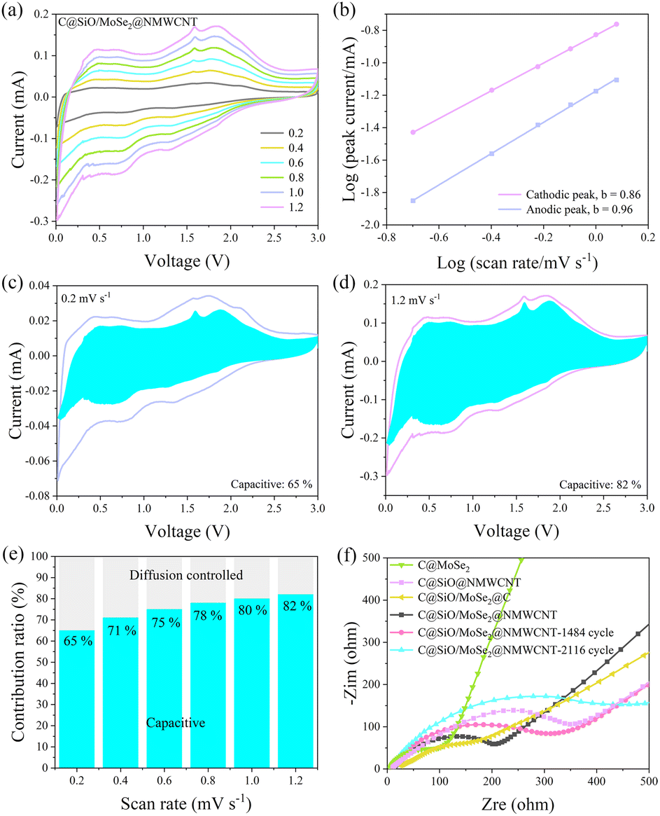 | ||
| Fig. 7 (a) CV curves of C@SiOx/MoSe2–3:1@NMWCNT, (b) curves of log (scan rate) versus log (peak current), (c) and (d) Pseudocapacitive contribution of C@SiOx/MoSe2–3:1@NMWCNT (0.2&1.2 mV s−1), (e) Pseudocapacitive contribution of C@SiOx/MoSe2–3:1@NMWCNT, (f) Nyquist plots of C@MoSe2, C@SiOx@NMWCNT, C@SiOx/MoSe2@C, C@SiOx/MoSe2–3:1@NMWCNT, C@SiOx/MoSe2–3:1@NMWCNT-1484 cycle and C@SiOx/MoSe2–3:1@NMWCNT-2116 cycle. | ||
As shown in Fig. 7b, the b-values of C@SiOx/MoSe2–3:1@NMWCNT composites at the anode and cathode are 0.96 and 0.86. It implies that this belongs to the pseudocapacitance process when the b-value is near 1.46 The capacitance contribution ratio of C@SiOx/MoSe2–3:1@NMWCNT can be analyzed using eqn (4):
| i(v) = k1v + k2v0.5 | (4) |
In eqn (4), k1v and k2v0.5 represent the capacitance-controlled behavior and diffusion-controlled behavior, respectively. According to Fig. 7c and d, when the scan speeds were 0.2 and 1.2 mV s−1, the capacitance contributions were 65% and 82%, respectively. As shown in Fig. 7e, the capacitance contribution rates are 65%, 71%, 75%, 78%, 80% and 82% at scanning speeds ranging from 0.2 to 1.2 mV s−1, which is in an increasing trend. These results confirm that the capacitive control process significantly contributes to the total capacity of the electrode at elevated scan rates.
The electrical and chemical interactions of the C@MoSe2, C@SiOx@NMWCNT, C@SiOx/MoSe2@C, C@SiOx/MoSe2–3:1@NMWCNT, C@SiOx/MoSe2–3:1@NMWCNT-1484 cycle, and C@SiOx/MoSe2–3:1@NMWCNT-2116 cycle materials underwent analysis via electrochemical impedance spectroscopy (Fig. 7f). The Nyquist plots comprise a semicircle in the high-frequency range, which is indicative of the charge transfer impedance (Rct) between the electrode and the electrolyte, along with a low-frequency area that represents the sodium diffusion impedance (Zw). In Fig. 7f, the Rcts for the C@MoSe2, C@SiOx@NMWCNT, C@SiOx/MoSe2@C, C@SiOx/MoSe2–3:1@NMWCNT, C@SiOx/MoSe2–3:1@NMWCNT-1484 cycle, and C@SiOx/MoSe2–3:1@NMWCNT-2116 cycle are 107, 359, 204, 212, 328, and 492 Ω, respectively. The results indicate that the incorporation of NMWCNT elevates the charge transfer impedance, suggesting a robust interaction between SiOx/MoSe2 and NMWCNT. When C@SiOx/MoSe2–3:1@NMWCNT was used as the electrode material, the Rct increased only significantly after 2116 cycles, suggesting that the material exhibited excellent cycling stability.
Fig. 8a shows the Nyquist plots for the C@MoSe2, C@SiOx@NMWCNT, C@SiOx/MoSe2@C, C@SiOx/MoSe2–3:1@NMWCNT, C@SiOx/MoSe2–3:1@NMWCNT-1484 cycle, and C@SiOx/MoSe2–3:1@NMWCNT-2116 cycle, used for calculating the sodium diffusion coefficient (D) according to eqn (5):
| D = R2T2/2A2n4F4C2σ2 | (5) |
| Zreal = Re + Rct + σω−1/2 | (6) |
:1@NMWCNT, C@SiOx/MoSe2–3:1@NMWCNT-1484 cycle, and C@SiOx/MoSe2–3:1@NMWCNT-2116 cycle were 2259, 3316, 1137, 1130, 814, and 1710, respectively. Then, the D of C@MoSe2, C@SiOx@NMWCNT, C@SiOx/MoSe2@C, C@SiOx/MoSe2–3:1@NMWCNT, C@SiOx/MoSe2–3:1@NMWCNT-1484 cycle, and C@SiOx/MoSe2–3:1@NMWCNT-2116 cycle were calculated to be 4.130787205996194 × 10⁻¹⁸ cm2 s−1, 1.917062364763804 × 10⁻¹⁸ cm2 s−1, 1.63058842731859 × 10⁻¹⁷ cm2 s−1, 1.650852980340063 × 10⁻¹⁷ cm2 s−1, 3.18138680371784 × 10⁻¹⁷ cm2 s−1, 7.208967445012913 × 10⁻¹⁸ cm2 s−1. This indicates that the sodium-ion mobility of the C@SiOx/MoSe2–3:1@NMWCNT is stronger than that of the C@MoSe2, C@SiOx@NMWCNT and C@SiOx/MoSe2@C. More interestingly, the sodium-ion mobility of the C@SiOx/MoSe2–3:1@NMWCNT composites after 1484 cycles was higher than that before cycling. The C@SiOx/MoSe2–3:1@NMWCNT composites were further validated for their exceptional performance and robust cycling stability.
 | ||
| Fig. 8 (a) Nyquist plots of the C@MoSe2, C@SiOx@NMWCNT, C@SiOx/MoSe2@C, C@SiOx/MoSe2–3:1@NMWCNT, C@SiOx/MoSe2–3:1@NMWCNT-1484 cycle and C@SiOx/MoSe2–3:1@NMWCNT-2116 cycle, and (b) functional relation diagrams of Zre (Zreal) and ω−1/2. | ||
Conclusions
In summary, we describe a straightforward method for synthesizing C@SiOx/MoSe2@NMWCNT three-layer heterojunction materials based on NMWCNTs. The three-layer heterojunction structure within the composite system is capable of not only efficiently accommodating the volume fluctuations of SiOx/MoSe2 but also preserving the structural stability of the electrode, thereby improving the conductivity of sodium ions and electrons, but also making the high-capacity SiOx uniformly dispersed in the MoSe2 nanosheet framework. When used as a stand-alone electrode, the optimized C@SiOx/MoSe2–3:1@NMWCNT material provides high capacity (526 mA h g−1 after 300 cycles at 500 mA g−1) and robust cycling stability (373 mA h g−1 after 2000 cycles at 5A g−1 and 353 mA h g−1 after 3000 cycles, 177.79 mA h g−1 after 3000 cycles at 10 A g−1). The good characteristics of this composite can be attributed to these underlying factors. First, high-capacity silicon was added to the composite system, and the two-dimensional (2D) MoSe2 nanoflap played the role of dispersing silicon, which improved the discharge capacity and rate performance of the C@SiOx/MoSe2@NMWCNT composites. The second is the formation of three-dimensional heterojunction materials, NMWCNT and externally coated carbon, which provide a specific space for SiOx/MoSe2, which can alleviate the volume expansion caused by the detachment and intercalation of Na+ and increase the cyclic durability of the composites. The newly devised synthesis technique can be used to design electrode materials intended for the fabrication of SIBs.
Experimental
Materials and methods
First, ethylene glycol (15 mL) and MoCl5 (27.2 mg) were mixed for four hours of sonication and then poured into a ceramic ark filled with Se (24 mg) and calcined to 800 °C in a tube furnace to prepare C@MoSe2 (12.37 mg). The yield of the anode material was 44% (based on Mo element), 33% (based on Se element).
As in the above process, ethylene glycol (15 mL) and triphenylchlorosilane (88.2 mg) were mixed to form a mixed solution (ultrasonic until completely dissolved). NMWCNTs (8 mg) were then added, and ultrasonication was continued for 4 h. Finally, this mixed solution was poured into a ceramic ark and calcined to 800 °C in a cylindrical furnace to prepare C@SiOx@NMWCNT (12.1 mg), and the yield of the anode material was 5.9% (based on Si element).
As above, MoCl5 (27.2 mg) was first dissolved in ethylene glycol (8.5 mL), then triphenylchlorosilane (58.8 mg) and ethylene glycol (11.5 mL) were added to ultrasonic for four hours and then poured into the ceramic ark filled with Se (24 mg) and calcined to 800 °C in a cylindrical furnace to prepare C@SiOx/MoSe2@C (26.4 mg); the yield of anode material was 91% (based on Mo element), 66% (based on Se element), and 7.8% (based on Si element).
In the same way, when SiOx and MoCl5 were in different proportions (1:1, 2:1, 3:1, 4:1, 5:1), MoCl5 (27.2 mg) was first separately dissolved in a certain amount of ethylene glycol (10 mL, 8.5 mL, 5.6 mL, 6 mL, 6 mL), then different amounts of triphenylchlorosilane (29.4 mg, 58.8 mg, 88.2 mg, 117.6 mg, 147 mg) and ethylene glycol (5.6 mL, 11.5 mL, 17 mL, 20 mL, 22 mL) were separately added to ultrasonic for four hours and then poured into the ceramic ark filled with Se (24 mg) and calcined to 800 °C in a tube furnace to prepare C@SiOx/MoSe2@NMWCNT (32 mg, 29.06 mg, 33.9 mg, 29.86 mg, 33.89 mg). The composites obtained with different ratios of SiOx and MoCl5 were respectively named C@SiOx/MoSe2–1:1@NMWCNT, C@SiOx/MoSe2–2:1@NMWCNT, C@SiOx/MoSe2–3:1@NMWCNT, C@SiOx/MoSe2–4:1@NMWCNT and C@SiOx/MoSe2–5:1@NMWCNT. When the ratio was 3:1, the yield of anode material is 77% (based on Mo element), 57% (based on the Se element), and 10% (based on the Si element).
The tube furnace was first heated for 2 h at 80 °C, then heated for 3 h at 180 °C, and finally heated for 4 h at 800 °C. The heating conditions are: heating rate of 5 °C min−1 and Ar heating atmosphere.
Material characterization
The scanning electron microscope SEM (S-4800 & IGMAHD) and transmission electron microscope TEM (JEM-2100F) were used to observe the morphology of the materials. The structure of the substance was observed by X-ray photoelectron spectroscopy AXIS SUPRA (SHIMADZU), X-ray powder diffraction with Bruker-D8 and Raman spectra Lab RAM Odyssey (HORIBA). The MoSe2 and SiOx contents were measured by thermogravimetry (STA7200 HITACHI).Fabrication of cells and electrochemical measurements.
Initially, C@MoSe2, C@SiOx@NMWCNT, C@SiOx/MoSe2@C, or C@SiOx/MoSe2@NMWCNT are blended with carboxyl methylated cellulose and carbon black, each in a mass ratio of 4:1:1. Then, a suitable quantity of deionized water and ethanol was added and stirred to produce a mixed slurry. Finally, the slurry was evenly applied to the copper foil. Subsequently, it was dried inside a vacuum oven used for drying and then cut to obtain electrode sheets. The electrode sheets, electrolyte, separator, sodium metal and CR2032 coin cells were then assembled into batteries. Sodium-ion batteries are made in a glove box with an Ar atmosphere, and the concentration of water and oxygen within the glove box should be less than 0.5 ppm. The electrolyte consisted of 1 M NaClO4 dissolved in a mixture with a 1:1 EC/PC volume ratio containing 5% FEC and a fiberglass separator. After assembling the batteries, they were tested for cycling and rate performance using the Neware test system with a voltage range of 0.01–3.0 V (vs. Na+/Na), and a range of current densities was employed during the testing process. Cyclic voltammetry (CV) and alternating current impedance (AC-Impedance) measurements were performed using a CH Instrument model CHI 660E.
Data availability
The data supporting this article are included in the ESI.†Author contributions
Conceptualization: RQ, MB, YY, YC, WD; methodology: RQ, MB, YY, TW, YC, WD; investigation: MB, YY, TW, BF, YC; project administration: RQ; writing – original draft: RQ, MB; writing – review & editing: RQ, MB, YY, YC, WD.Conflicts of interest
MB and YY contribute equally.Acknowledgements
The authors thank the National Natural Science Foundation of China (21878071, 22278120 and U24A20539), the Program sponsored by the Foundation of YueLuShan Center Industrial Innovation (2023YCII0127) for financial support. The authors thank Prof. Wai-Yeung Wong (Hongkong Polytech University), Prof. Shuang-Feng Yin and Prof. Shiguo Zhang (Hunan University), and Prof. Zhenqiang Yu (Shenzheng University) for helpful discussion.Notes and references
- H. Z. Niu, N. Zhang, Y. Lu, Z. Zhang, M. N. Li, J. X. Liu, N. Zhang, W. Q. Song, Y. Z. Zhao and Z. C. Miao, J. Energy Storage, 2024, 88, 111666 Search PubMed.
- X. Liu, T. Y. Zhang, X. X. Shi, Y. Ma, D. W. Song, H. Z. Zhang, X. Z. Liu, Y. G. Wang and L. Q. Zhang, Adv. Sci., 2022, 9, 2104531 CAS.
- C. Y. Wang, C. P. Yang and Z. J. Zheng, Adv. Sci., 2022, 9, 2105213 CAS.
- Y. Q. Luo, Y. J. Tang, S. S. Zheng, Y. Yan, H. Q. Xue and H. Pang, J. Mater. Chem. A, 2018, 6, 4236–4259 CAS.
- P. T. Bhutia, S. Grugeon, A. EI Mejdoubi, S. Laruelle and G. Marlair, Batteries, 2024, 10, 370 CAS.
- Y. You and A. Manthiram, Adv. Energy Mater., 2024, 10, 370 Search PubMed.
- L. Z. Wang, Q. M. Li, Z. Y. Chen, Y. T. Wang, Y. F. Li, J. L. Chai, N. Han, B. H. J. Tang, Y. C. Rui and L. Jiang, Small, 2024, 20, 2310426 CAS.
- D. Schäfer, K. Hankins, M. Allion, U. Krewer, F. Karcher, L. Derr, R. Schuster, J. Maibach, S. Mück, D. Kramer, R. Mönig, F. Jeschull, S. Daboss, T. Philipp, G. Neusser, J. Romer, K. Palanisamy, C. Kranz, F. Buchner, R. J. Behm, A. Ahmadian, C. Kuebel, I. Mohammad, A. Samoson, R. Witter, B. Smarsly and M. Rohnke, Adv. Energy Mater., 2024, 14, 202302830 Search PubMed.
- Z. Zhang, X. Yang, Y. Fu and K. Du, J. Power Sources, 2015, 296, 2–9 CrossRef CAS.
- M. Y. He, S. M. Liu, J. T. Wu and J. L. Zhu, Prog. Solid State Chem., 2024, 74, 100452 CrossRef CAS.
- H. Zhou, J. Z. Liu, L. S. Guo, J. Y. Zhang, S. Feng and X. M. Zhang, Colloids Surf., A, 2022, 648, 129386 CrossRef CAS.
- P. Nie, Z. Y. Le, G. Chen, D. Liu, X. Y. Liu, H. B. Wu, P. C. Xu, X. R. Li, F. Liu, L. M. Chang, X. G. Zhang and Y. F. Lu, Small, 2018, 14, 1800635 CrossRef PubMed.
- Y. Q. Tao, Q. Y. Zhou, C. J. Cai, C. Y. Song, H. Li, X. Huang, L. J. Yang, W. Huang and S. Z. Li, Energy Environ. Sci., 2021, 14, 6672–6677 RSC.
- M. B. Huai, X. M. Li, Y. Zhang, X. M. Qin, Y. F. Zhang, X. Y. Qin, Y. F. Liu, X. X. Liang, G. Li and J. B. Zhao, ChemCatChem, 2024, 17, e202401651 CrossRef.
- H. J. Chen, Z. M. Li, Z. X. Qin, H. J. Kim, H. Abroshan and G. Li, ACS Appl. Nano Mater., 2019, 2, 2999–3006 CrossRef CAS.
- J. B. Zhao, X. M. Li, M. Zhang, Z. Xu, X. M. Qin, Y. F. Liu, L. F. Han and G. Li, Nanoscale, 2023, 15, 4612 RSC.
- L. H. Zhang, Y. Z. Liu, B. Key, S. E. Trask, Z. Z. Yang and W. Q. Lu, ACS Appl. Mater. Interfaces, 2017, 9, 32727–32736 CrossRef CAS PubMed.
- Y. Hwa, C. M. Park and H. J. Sohn, J. Power Sources, 2013, 222, 129–134 CrossRef CAS.
- J. H. Kim, A. R. Song, J. M. Park, J. S. Park, S. Behera, E. M. Cho, Y. C. Park, N. Y. Kim, J. W. Jung, S. J. Lee and H. S. Kim, Adv. Mater., 2024, 36, 2309183 CrossRef CAS PubMed.
- J. Woo, S. H. Baek, J. S. Park, Y. M. Jeong and J. H. Kim, J. Power Sources, 2015, 299, 25–31 CrossRef CAS.
- D. J. Lee, M. H. Ryou, J. N. Lee, B. G. Kim, Y. M. Lee, H. W. Kim, B. S. Kong, J. K. Park and J. W. Choi, Electrochem. Commun., 2013, 34, 98–101 CrossRef CAS.
- Y. Q. Lu, Z. M. Zou, Y. Bai and C. H. Jiang, Appl. Surf. Sci., 2024, 642, 158593 CrossRef CAS.
- N. Ishii, N. Kakinuma and H. Morimoto, Electrochemistry, 2024, 92, 017006 CrossRef CAS.
- G. G. Kumar, M. K. Francis, P. B. Bhargav and N. Ahmed, Int. J. Hydrogen Energy, 2024, 51, 1448–1461 CrossRef.
- F. F. Cao, J. W. Deng, S. Xin, H. X. Ji, O. G. Schmidt, L. J. Wan and Y. G. Guo, Adv. Mater., 2011, 23, 4415–4420 CrossRef CAS PubMed.
- J. J. Ma, H. Zhang, R. Q. Liu, W. Q. Zhang, S. X. Han, J. Han, G. R. Xu, L. S. Li, Y. S. He and Z. F. Ma, Sci. China Mater., 2022, 66, 493–504 CrossRef.
- Q. Zhong, K. J. Zhou, Z. Y. Yang and J. Yu, J. Energy Storage, 2024, 97, 112784 Search PubMed.
- T. H. Yao, H. K. Wang, X. Ji, D. Y. Wang, Q. M. Zhang, L. J. Meng, J. W. Shi, X. G. Han and Y. H. Cheng, Small, 2023, 19, 2302831 CrossRef CAS PubMed.
- Y. Li, F. Wu, Y. Li, X. Feng, L. M. Zheng, M. Q. Liu, S. Q. Li, J. Qian, Z. H. Wang, H. X. Ren, Y. T. Gong, C. Wu and Y. Bai, Adv. Mater., 2024, 36, 2310270 CAS.
- M. Shimizu, H. Usui, K. Fujiwara, K. Yamane and H. Sakaguchi, J. Alloys Compd., 2015, 640, 440–443 CAS.
- C. L. Ma, Y. H. Wang, N. J. Song, Z. R. Wang, F. Zhang, S. Q. Li, Q. Zhang, Y. Li and Y. Zhao, Int. J. Energy Res., 2022, 46, 15912–15925 CAS.
- T. Hirono, H. Usui, Y. Domi, W. Irie, T. Nishida, T. Sawada and H. Sakaguchi, Electrochemistry, 2023, 91, 017001 CAS.
- C. H. Lim, T. Y. Huang, P. S. Shao, J. H. Chien, Y. T. Weng, H. F. Huang, B. J. Hwang and N. L. Wu, Electrochim. Acta, 2016, 211, 265–272 CAS.
- M. Yousaf, Y. S. Wang, Y. J. Chen, Z. P. Wang, A. Firdous, Z. Ali, N. Mahmood, R. Q. Zou, S. J. Guo and R. P. S. Han, Adv. Energy Mater., 2019, 9, 1900567 CrossRef.
- N. Abharana, K. K. Halankar, A. Pathak and D. Bhattacharyya, J. Alloys Compd., 2024, 976, 173096 CrossRef CAS.
- H. Wang, X. Z. Lan, D. L. Jiang, Y. Zhang, H. H. Zhong, Z. P. Zhang and Y. Jiang, J. Power Sources, 2015, 283, 187–194 CrossRef CAS.
- F. Wang, M. R. Bian, Y. C. Yang, S. G. Zhang, Z. Q. Yu, C. T. Au, S. F. Yin and R. H. Qiu, J. Alloys Compd., 2023, 963, 171175 CrossRef CAS.
- Y. C. Yang, F. Wang, M. R. Bian, Y. W. Chen, S. G. Zhang, Z. Q. Yu, C. T. Au, S. F. Yin and R. H. Qiu, Electrochim. Acta, 2023, 461, 142598 CrossRef CAS.
- A. C. Joshi, D. P. Dutta, R. Alexander, M. Roy and K. Dasgupta, ChemNanoMat, 2024, 10, e202400014 CrossRef CAS.
- M. Yousaf, Y. S. Wang, Y. J. Chen, Z. P. Wang, W. Aftab, A. Mahmood, W. Wang, S. J. Guo and R. P. S. Han, ACS Appl. Mater. Interfaces, 2018, 10, 14622–14631 CrossRef CAS PubMed.
- S. W. Li, L. Wu, J. J. Zhao, R. X. Li, H. L. Yang, L. M. Zhao and R. F. Jin, Green Chem., 2023, 25, 10033–10042 RSC.
- S. K. Singh, K. Takeyasu and J. Nakamura, Adv. Mater., 2019, 31, 1804297 CrossRef PubMed.
- M. X. Liang, N. N. Liu, X. C. Zhang, Y. Xiao, J. H. Yang, F. Yu and J. Ma, Adv. Funct. Mater., 2022, 32, 2209741 CrossRef CAS.
- Y. C. Yang, F. Wang, Y. W. Chen, C. M. Chen, S. G. Zhang, Z. Q. Yu, C. T. Au, S. F. Yin and R. H. Qiu, Sci. China: Chem., 2023, 66, 475–491 CrossRef CAS.
- X. P. Yi, X. L. Liu, J. Fang, H. L. Huo, R. F. Dou, Z. Wen and W. N. Zhou, Appl. Surf. Sci., 2023, 615, 156367 CrossRef CAS.
- Y. C. Yang, F. Wang, M. R. Bian, Y. W. Chen, S. G. Zhang, Z. Q. Yu, C. T. Au, S. F. Yin and R. H. Qiu, J. Alloys Compd., 2024, 984, 173926 CrossRef CAS.
- V. T. Phat, C. T. M. Thu, N. T. Trung, L. M. L. Phung and W. Kaveevivitchai, Int. J. Energy Res., 2022, 46, 21727–21738 CrossRef CAS.
- X. Chen, L. Monconduit and V. Seznec, Electrochim. Acta, 2023, 462, 142756 CrossRef CAS.
Footnotes |
| † Electronic supplementary information (ESI) available: Additional TEM images. See DOI: https://doi.org/10.1039/d4lf00399c |
| ‡ MB and YY contribute equally. |
| This journal is © The Royal Society of Chemistry 2025 |