
 Open Access Article
 This Open Access Article is licensed under a
 Creative Commons Attribution 3.0 Unported Licence
Promoting combined AFM-electrochemistry techniques for analysis of charge transport at grain boundaries of ceramic components in electrochemical cells
K.
Neuhaus
 *a,
P.
Mowe
a and
M.
Winter
ab
*a,
P.
Mowe
a and
M.
Winter
ab
aForschungszentrum Jülich GmbH, Institute of Energy Materials and Devices IMD-4: Helmholtz-Institute Münster (HI MS), Münster, Germany. E-mail: k.neuhaus@fz-juelich.de
bUniversity of Münster, MEET Battery Research Center, Institute of Physical Chemistry, Münster, Germany
First published on 11th March 2025
Abstract
For decades, the differences between the transport properties of grains and grain boundaries in polycrystalline oxides have been widely discussed in the scientific community. The reason is that grain boundaries, although representing a much smaller fraction of a given material than the grain interior, can greatly influence the performance of ceramic materials, which is a major drawback for the industrial application of these materials. Detailed knowledge of the chemical and physical parameters at the interfaces between adjacent grains is required in order to develop targeted synthesis strategies that specifically influence the transport properties of grain boundaries. Atomic force microscopy (AFM)-based electrochemical methods use an nm-sized tip as a probe and are able to image, for example, band bending at grain boundaries or variations in electrical conductivity with extremely high local resolution, thus providing small-scale insights into the physical and electrochemical conditions at grain boundaries. The results obtained by AFM-based electrochemical experiments are complementary to conventional electrochemical measurements and facilitate detailed modeling of grain boundary parameters in different materials. In this work, the differences between grain boundaries and grain interiors with respect to charge transport properties are first discussed with a special focus on oxide ion conducting and proton conducting materials. In a second step, a broader perspective on current research and potential applications of AFM-based grain boundary analysis in the field of lithium-ion battery materials is given.
1 Introduction
Atomic force microscopy (AFM) is a measurement technique which was invented by Binnig, Quate and Gerber in 1986.1 It evolved from scanning tunneling microscopy and can primarily be used to measure the topography of a given sample. Basically, a very fine tip with a diameter in the range of a few nm, which is attached to a cantilever, is scanned along a sample surface. The position of the cantilever is controlled by a laser positioning system where a laser beam is reflected off the back of the cantilever, and the reflection is then captured by a photodetector. The possible resolution for AFM topography measurements depends on the tip diameter, but is typically in the nm range in the x and y directions and in the pm range in the z direction. By monitoring the tilt and torsional motion of the cantilever and tip, additional information about the surface roughness and elasticity can be obtained.AFM measurements are possible in three basic modes: i) contact mode, where the tip remains in contact with the sample surface throughout the whole experiment, ii) intermittent contact mode, where the cantilever vibrates at its resonance frequency (typically in the kHz-range) and taps the sample surface at regular intervals during scanning, and iii) non-contact mode, where the tip is moved at a constant distance above the surface, allowing interaction between the tip and short-range physical attractive and repulsive forces of the sample surface.2
The AFM technique has been rapidly diversified, for instance by the use of conductive AFM tips, which allow to image different physical properties like electrical conductivity or local surface potential distribution and to correlated them with the sample topography. Due to the very high resolution, AFM-based methods are well-suited to measure a range of different parameters at very tiny interfaces and have been used more and more frequently in the last decade to shed light on the complex topic of charge carrier transport and defect concentrations at grain boundaries and similar interfaces.3–5
The present work focuses on AFM-based electrochemical methods and their application for measurements of grain boundary related variations in transport behavior and defect concentrations in oxidic oxide-ion, proton, and lithium-ion conductors. Corresponding measurement techniques have already been successfully applied for example in the field of solar cell materials,6,7 where grain boundaries play an important role in charge transport, although the focus here is on electron/hole transport rather than ion transport.
The overall goal of this perspective is, on the one hand, to show how valuable AFM-based electrochemical measurements can be for determining small-scale electrochemical interactions at very small interfaces. On the other hand, challenges and opportunities for AFM-based studies of charge transport at grain boundaries are identified.
2 Theoretical background and methods
2.1 Differences in transport characteristics between grain interior and grain boundaries
In a first instance, grain boundaries represent confined zones with a structural mismatch due to differing crystallographic orientations between adjacent grains. However, grain boundaries can have strongly different transport characteristics for ions and/or electrons compared to the bulk of a given material. This can have different reasons, which are discussed in the following sections.The width of these space-charge layers is typically larger in low-dopant systems due to reduced screening effects, as fewer mobile charge carriers are available.20,21 The description of dilute systems assumes constant defect mobilities in grain boundaries and grain interiors, whereby the defect concentrations differ. However, defect–defect or defect–dopant interactions are neglected here, which increasingly influence the transport properties at higher doping concentrations.22 Various studies have already shown that the agreement between theory and experiment, which works quite well with dilute materials, is insufficient for higher dopant concentrations.23,24 However, materials with low doping concentrations are not suitable for a range of applications such as fuel cells, battery storage or sensors due to their low ionic conductivity. D. S. Mebane and R. A. De Souza25 were able to solve this problem and extended the theoretical framework to predict experimental point-defect behavior at grain boundaries in concentrated solid solutions. By combining the Poisson–Boltzmann approach to describe defect behavior near interfaces with the Cahn–Hilliard model for concentrated solid solutions they achieved good accordance between their model and experimental values from impedance spectroscopy measurements.
Impedance spectroscopy is the most common method for measuring the lateral extent of space-charge regions. Other possibilities to investigate dopant segregation26 and also to directly observe local grain boundary potential barriers are transmission electron microscopy based methods (e.g. atom tomography).27 Here, the advantage is the possible combination with measurements of the local chemical composition, but the disadvantages are the difficult sample preparation (ion beam milling, FIB lamellae preparation etc.) and high costs of the TEM instrumentation.
Recently, S. Kim and co-workers31 established an impedance spectroscopy-based method to determine the contribution of space-charge vs. insulating layers on the grain boundary resistivity in proton and oxide-ion conducting ceramic with low dopant concentrations. Apart from that, it is difficult to study the transport properties of individual grain boundary phases with conventional electrochemical methods due to their very low thickness. For both dilute and high doping concentrations, but also for materials with secondary phases at the grain boundaries, AFM-based measuring methods are suitable as complementary techniques for analyzing the grain boundaries. On the one hand, they can act as a nanocontact for conventional electrochemical measurements due to their small contact diameter. On the other hand, special measuring methods such as Kelvin probe force microscopy (KPFM) or Electrochemical Strain Microscopy (ESM) can provide direct information about the height and width of the potential barrier at grain boundaries or enable high-resolution measurements of ionic conductivity. Details will be discussed in chapter 2.2 and 3.
Ceramic proton and oxide-ion conductors work at ideal operation temperatures between 400–900 °C. Since most AFM-based observations are conducted in a low-temperature regime, typically below 200 °C, or even at sub-room temperature, impedance spectroscopy measurements of ceramics can be performed at optimal operating temperatures. For materials with high application temperatures, AFM-based measurements at room temperature therefore only provide limited information, but can be used to complement measurements at the corresponding application temperatures. There are some AFM measurement setups that can also work at temperatures well above 200 °C,33,34 but then there are problems with, for example, the conductive coating or the very fine AFM tips that cannot easily withstand these temperatures. Meanwhile, AFM-based measurement methods are ideally suited for battery materials that already exhibit very good conductivity within the range of ambient temperature.35,36
2.2 AFM-based electrochemical measurement techniques
AFM-based electrochemical measurements allow for measurement as well as visualization of different grain boundary characteristics (see also Fig. 1). For this kind of measurements, typically an AFM tip coated with Pt or Au is used to make it conductive. Other than in most conventional electrochemical measurement techniques which apply macroscopic electrodes, a conductive AFM tip offers the possibility to gather information on different parameters with a high lateral resolution and simultaneously correlate the results to topographical attributes of the sample. This means that grain boundaries can be easily identified on crystalline samples which have not undergone a surface treatment, as grain boundaries appear as small trenches in the topography (similarly as in light or electron microscopy images). In the following, the four most important AFM-based measurement techniques in this context will be broadly introduced. An overview can also be found in Table 1. | ||
| Fig. 1 Schematic overview of possibilities of grain boundary characterization using AFM-based measurement techniques. Right: The AFM tip is scanned over an idealized ceramic material with differently sized grains. The defect concentration varies from bulk to grain boundaries. Right: Apart from the sample topography, AFM-based analysis methods allow directly obtaining or calculating important physical characteristics associated with the defect concentration variations. | ||
| Technique | Common abbreviations | Measurand |
|---|---|---|
| Conductive AFM | CAFM, CS-AFM | Local electrical conductivity |
| Electrochemical strain microscopy | ESM | Change in surface morphology due to ion movement induced by applied voltage |
| Kelvin probe force microscopy | KPFM, KFM, SKPM | Local contact potential difference between metal coated tip and sample surface |
| Scanning microwave impedance microscopy | sMIM, SMM | Complex impedance → resistance |
ESM can be divided into two main spectroscopy methods, the time spectroscopy and the voltage spectroscopy. While in time spectroscopy the signal is measured after a short voltage pulse and normally is detected over a longer time, in voltage spectroscopy the signal is measured during each pulse of increasing and decreasing voltage.
It is possible to detect several different signals. Information about the surface are similar to other standard AFM techniques and are mainly described by the height and phase signal. The topography shows an image of the sample by scanning the surface with the AFM tip and depicts the differences in both lateral and height difference, the height information is directly connected to the change of the AFM z-piezo. The phase signal is sensitive to the stiffness of the surface as well as to the adhesion between tip and sample. Both signals (height and phase) are detected in intermitting contact mode (AC mode). The ESM amplitude signal gives information about the change of the strain while applying different bias pulses,47 either with comparably low frequency or in the high frequency regime. This signal is detected while the AFM tip is directly in contact with the surface and is based on the deflection of the cantilever, which means that variations in the pm-range can be detected. An increasing ESM amplitude signal means that the surface height is increasing locally and vice versa.
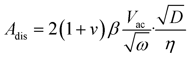
Based on the assumption that ion transport processes in the sample material are diffusion-limited and that the contribution of migration is minimal, the amplitude of the oscillating surface displacement Adis, in units of distance, is (in the high-frequency regime):
 | (1) |
 | (2) |
| ΔφCPD = φtip − φsmp | (3) |
The KPFM signal can be calibrated using a reference sample with a well-established work function like for example HOPG, thus yielding absolute values for the contact potential difference. Then, a correlation of the Volta potential at the probe location and surface Fermi energy EFS can be established by:
| EFS = EVac − Vtip − φtip | (4) |
In many cases, KPFM studies are not executed in vacuum but in air, so an influence of adsorbed water and other adsorbed species on the measurement signal cannot be ruled out. Water acts as a dipole which can be aligned for example in an electric field and which can have an additional effect on the KPFM signal.56
Apart from conventional impedance spectroscopy methods, there are two other impedance spectroscopy-related AFM-based methods: Keysight, USA and Oxford Instruments, UK offer Scanning Microwave Microscopy (SMM) and Scanning Microwave Impedance Microscopy (sMIM), respectively, which are measurement techniques utilizing an external microwave signal in the GHz range to measure the complex impedance of a sample. To achieve this, in contact mode, the signal is conducted through the AFM tip onto the surface of the sample and the diffracted signal is monitored. During scanning, local sample variations in permittivity (ε) and conductivity (σ) affect the reflected microwaves and can be analyzed. Typical penetration depths are in the range of 80 nm to 120 nm, depending on the materials. Respective techniques have already been used to measure charge carrier mobility in different semi-conductive materials or electrolytes60,61 and even for observation of grain boundary characteristics in electron conductors such as solar cell materials62 or ferrites,63 but comprehensive studies on grain boundaries of ion conductive, oxidic materials are very scare so far. However, the measurement approach would be extremely interesting for a variety of different questions with relation to defect concentration distribution at grain boundaries.
3 AFM analysis of grain boundaries in oxide-ion and proton conductive oxides
Oxide ion conductive ceramics normally work at elevated application temperatures compared to those typically used for solid oxide electrolyzers, lithium ion batteries or semi-conductors. Typical temperatures range from 600–1000 °C with ceria-based materials at the low temperature end, perovskites like (La,Sr)(Co,Fe)O3 (LSCF) and (Ba,Sr)(Co,Fe)O3 (BSCF, see also Fig. 2) in the low to middle temperatures and yttria-stabilized zirconia (YSZ) at the high temperature end. Apart from very few exceptions,33,34,64 these temperatures cannot be accessed by AFMs, hence AFM-based research has to focus on temperatures where the oxygen vacancies only show very low mobility or are completely frozen.65,66 Nevertheless, near-surface defects can still be mobile and, for example, participate in catalytic reactions and proton conductivity in oxide-ion conductors also occurs at lower temperatures than oxide-ion conductivity.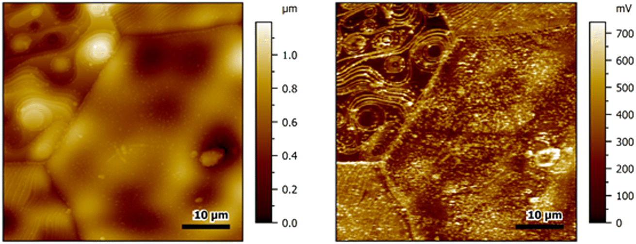 | ||
| Fig. 2 Topography (left) and corresponding KPFM image (right) of a Ba0.5Sr0.5Co0.8Fe0.2O3 ceramic pellet with very large grains. The grain boundaries appear as lines with markedly increased potential and also step faults show light potential differences. Measurements were performed with PPP-NCSTPt tips in a single-pass amplitude modulation mode in lab air. | ||
There has not been much scientific work published with regards to AFM-based measurements specifically on proton conductive oxides. However, predominantly oxide-ion conductive materials like ceria and zirconia have shown to transport protons via the surface in the low to intermediate temperature regions.67–70
3.1 Perovskite proton and oxide ion conductors
Y-doped BaZrO3 (especially the composition BaZr0.9Y0.1O3−δ) has one of the highest reported bulk proton conductivities compared with other perovskite materials (6.5 mS cm−1 at 650 °C in wet air)71 and it also shows a higher chemical and mechanical stability than corresponding cerate-based materials, especially when exposed to CO2. Similar to the oxygen ion conductive materials described in section 5, BaZrO3 and its acceptor-doped derivatives have been shown to develop a net positive charge at the grain boundaries with an adjacent negatively charged SCL. The positive charge at the grain boundary core is counteracted by segregation of the acceptor dopant, therefore a higher acceptor dopant concentration leads to a decreased potential barrier height at the grain boundaries, hence space-charge layers are mainly relevant for dilute defect concentrations. The situation is easily comparable to the one for oxide-ion conductive materials, as BaZrO3 and related perovskite proton conductors also show oxide-ion conductivity at elevated temperatures.Differences between the grain boundary potential barrier height calculated from eqn (1) under humid or dry conditions have been attributed to a grain boundary core hydration process (preferred absorption of protons at the grain boundary core defects when changing from dry to humid conditions).71 Also, a strong influence of the synthesis conditions is reflected in differing potential height barriers found for materials with the same compositions but different synthesis routes.71–74
Specific measurements of the potential barrier at the grain boundaries under different conditions using AFM-based methods have so far (to the knowledge of the authors) not been performed for BaZrO3-based materials, although the potential difference is high enough to make grains and grain boundaries easily distinguishable with AFM-based electrochemical measurement methods,71–74 but there are two AFM-based studies on proton transport which also are of interest for fully understanding the grain boundary characteristics in BaZrO3.
Yang et al.75 performed ESM measurements to detect the electrochemical activity of fully hydrated BaZr0.8Y0.2O3−δ thin films on NdGaO3 substrates, which show a 10% lattice mismatch. Local electrochemical results were complemented with scanning transmission electron microscopy (STEM) investigations to obtain information about local structural defects. The investigations showed a clear dependence between the local conductivity and local structural defects (introduced by lattice mismatch of thin film and substrate) at temperatures between RT and 110 °C, which is in good accordance to the idea that grain boundaries are main obstacles for proton transport in Y-doped BaZrO3. For the measurements, short polarization pulses with up to 42 V were used and the polarization–relaxation of the lattice strain was monitored using the local dilatation in z-direction. The obtained activation energies for samples with 300 nm film thickness were roughly comparable to literature results for the bulk transport (0.3 eV with ESM compared to roughly 0.4 eV obtained from literature by conventional electrochemical methods). Samples with a film thickness of 20 nm showed considerably decreased activation energies. This was attributed to a network of dislocations at the interface between thin film and substrate, which could increase the proton transport locally and have a major impact due to the low thickness of the film.
These findings are backed up by investigations by Ding et al.76 using time-resolved KPFM on epitaxial BaZr0.8Y0.2O3−δ thin films grown on MgO substrates. For their measurements, Ding et al. polarized their samples using sputtered micro contacts and performed a series of measurements before, during and after the polarization in order to measure polarization–relaxation effects on the surface potential. They were able to show that slightly Ba-deficient/Y-enriched thin films show a smaller local distortion accompanied by a decrease of proton-trapping effect and a higher proton mobility (Ba vacancies act as acceptor dopants on the A-side). Local enrichment of Y3+ cations has also been observed at the grain boundaries in Y-doped BaZrO3.
Apart from proton conducting perovskites, there is a huge variety of mixed oxygen ion and electron conductive perovskite compositions which have been published so far,77 the most prominent example being lanthanum strontium cobalt ferrate or La1−xSrxCo1−yFeyO3 (LSCF),78 which is a chemically stable and already widely applied oxygen ion conductor, and the related Ba1−xSrxCo1−yFeyO3 (BSCF). Compared to the proton conductive perovskites, both LSCF and BSCF show a very high electron conductivity, making them ideal materials for oxygen permeation membranes or electrodes in solid oxide fuel cells.77,79 Grain boundaries within LSCF and BSCF are characterized by segregation of Sr and Ba, which are mobile within the crystal structure at common application temperatures, but also, depending on the exact composition, by segregation of Co cations.80 However, there are no comprehensive AFM-based measurements of the height and extent of the potential barrier in corresponding materials.
3.2 Doped ceria and yttria-stabilized zirconia
As doped ceria as well as YSZ show ionic conductivities combined with – in case of ceria – a considerable electronic conductivity depending on the dopant, they have already been object of intense investigations. Due to the fluorite structure of both materials, physical and electrochemical characteristics are isotropic within a crystal.Previous studies confirmed that grain boundaries in acceptor doped ceria as well as YSZ13,81–84 can be described as double-Schottky layer, with the grain boundary core being positively charged with respect to the grain interior. The positive charge of the grain boundary core is thought to be counterbalanced by a diffuse SCL of negative charge (electrons or small polarons), which extends into the bulk of the grain similar to the structure confirmed for proton conductive oxides.
For YSZ, the positive net charge of the grain boundary core was found to be mainly produced by segregation of immobile oxygen vacancies,81 while for 10 cat% Gd-doped ceria an enrichment of Gd3+ in the first cation layer and an enrichment of positively charged, immobile oxygen vacancies  in the first anion layer of the grain surface was proposed based on simulations.85 In the surrounding SCL, a decreased concentration of mobile
  is found, while at the same time, the concentration of electrons is increased to compensate the positive net charge of the grain boundary core.84,86 The simulations were confirmed by a variety of AFM-based experiments: direct measurements of the grain boundary potential barrier by KPFM have already successfully been achieved for Gd-doped ceria87,88 confirming a potential barrier height in the area between 100–200 mV for 10 cat% acceptor doping, but strongly variable on a local scale depending on dopant concentration, inhomogeneities, crystal orientation etc. As can be seen from Fig. 3, the potential difference between grains and grain boundaries in 20 cat% Gd-doped ceria can still be perceived, but at a significantly reduced level. This is attributed to the phenomenon of reciprocal cancellation of effects at high dopant concentrations. In addition, combined polarization-KPFM measurements have been carried out on doped ceria and YSZ, which were used for the investigation of the surface exchange and local reduction–re-oxidation processes89–91 as well as gathering information about the effect of grain boundaries by comparison of the polarization–relaxation characteristics of nanocrystalline and epitaxial ceria thin films.92
 | ||
| Fig. 3 Top left: Topography measurements of 20 cat% doped CGO (Sigma Aldrich, USA), top middle: corresponding surface potential measurement by KPFM, where grain boundaries can be observed as faint outline with higher potential, top right: average grain boundary potential for 50 grain boundaries, the grain boundary potential barrier is in the range of the noise. Bottom left: Topography measurements of 10 cat% doped CGO (Treibacher Industrie AG, Germany), bottom middle corresponding surface potential measurement by KPFM, where grain boundaries can be observed as clear outline with higher potential, bottom right: average grain boundary potential for 71 grain boundaries. The average grain boundary potential barrier height is about 100 mV. Both samples were measured as received using Pt-coated cantilevers (PPP-NCSTPt) with amplitude modulation mode in lab air. | ||
Doria et al.93 compared the effects of polarization between nanocrystalline and epitaxial Sm-doped ceria thin films using ESM. By measuring the local vertical strain during application of short bias pulses and the subsequent mechanical relaxation of the samples, which relate directly to changes in the local defect concentration, they were able to show the existence of space-charge regions at Sm-doped ceria grain boundaries as well as at the sample surface with high resolution. The results were later backed up by measurements by Chen et al., who used a similar measurement method at temperatures between 20–200 °C.94
3.3 ZnO – high electron conductivity paired with low proton conductivity
Pure ZnO is a cheap, non-toxic, transparent, n-type semi-conductive material for multi-purpose application,95,96 which also shows a slight proton conductivity. Historically, it has been commercially used as a pigment since the 19th century.97 In electronics, ZnO ceramics and thin films are additionally widely used for photovoltaic and light emitting applications98 and have also been proposed as material for other electronic components,96,99 especially LEDs.100,101 Apart from this, one of the most important applications of ZnO with additions of Bi2O3 and other oxides is as varistor material,102 as it shows highly nonlinear I–V-properties, which are caused by double-Schottky barriers formed at the grain boundaries of the material.103 Below a critical breakdown voltage, which is typically in the range of 3–4 V, charge transport across grain boundaries is almost purely capacitive and the boundary behaves like an insulator. Above the critical voltage, however, electron transport across the grain boundary becomes ohmic.It is already known that negative charges represented by cation vacancies 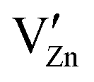 and
and 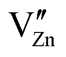 segregate at the grain boundary, while a positively charged SCL surrounds the grain boundary, including mainly oxygen vacancies
 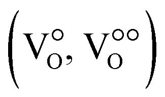 and zinc on interstitial lattice sites (
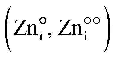 ), but also impurity donor cations at the place of Zn (
 , cf.Fig. 4).103,104 These cations can either be donor dopants or impurities like Bi or Sb, but it has been shown that protons or rather OH-groups at oxygen sites
 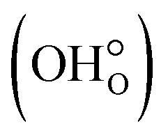 work as shallow donors in ZnO,105–107 increasing the electronic conductivity.
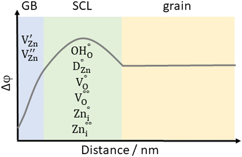 | ||
| Fig. 4 Scheme of the local Volta potential distribution at the grain boundary of ZnO, showing a complex interplay of different types of charged defects which are mobile to different extents. At the grain boundary, negative defects are abundant, while in the adjacent positive depletion layer, an increased concentration of positive defects can be found. | ||
AFM-based impedance spectroscopy methods have first been demonstrated using commercial ZnO varistor materials.58,59 It was found that a parallel resistor–capacitor equivalent circuit associated with transport in the grain boundary in addition to the Schottky contact build by the metallic tip and surface, provides the best description of the impedance spectroscopy data, which was to be expected from macroscopic results.
It has been shown by KPFM measurements that the potential barrier height at the grain boundaries of ZnO is strongly depending on the synthesis process,108 structure of the crystallites109 and substrate in case of thin films.110 For example Gonzalez-Julian et al.108 reported that an increase of the total proton concentration in a sample by wetting during sample synthesis (in this case spark plasma sintering) leads to an increase of positive charge in the space-charge region and also to an increase of negative charge in the direct vicinity of the grain boundary. This resulted in an increased potential barrier at grain boundaries and increased electronic conductivity along the grain boundaries. The results were confirmed by macroscopic impedance spectroscopy measurements.
Further, de Lucas-Gil et al.109 showed that by formation of star-shaped ZnO-particles consisting of stacked thin ZnO micro-platelets, the Schottky barrier character of the grain boundaries can be used to create negative charge accumulations by accumulating the band bending effect at the grain boundaries. The tips of the “stars” show an extremely high surface potential difference of up to 3.5 V between bulk and tips, which makes these particles suitable for antimicrobial applications. Similarly, Moreira et al.110 were able to confirm using a combination of EFM, KPFM and CAFM band bending in the range of 50 meV at grain boundaries of ZnO thin films.
4 Lithium ion conductors
From the previous section, it can be concluded that consistent results for the analysis of charge transport and the potential barrier at grain boundaries can be achieved in both oxide-ion or proton conducting oxide electrolytes and mixed ionic/electronic conductive (MIEC) using conventional and AFM-based measurement techniques. The AFM-based measurement methods, which have so far been used more as niche applications, are therefore a valid instrument for carrying out detailed spatially resolved analyses at grain boundaries and should also be recognized as such by the community. In the following, we would like to show that this can also be utilized for lithium-ion conducting materials, which are much more in the scientific and industrial focus.One of the key challenges for the design of efficient and long-living lithium batteries is to keep up a homogeneous Li-ion flow throughout several hundred charge and discharge cycles and throughout the full reaction area to prevent inhomogeneous lithium deposition, which is frequently called Li metal dendrite formation, which is a severe problem for battery safety. One reason for inhomogeneities of the lithium ion distribution can be internal interfaces in the solid electrolyte or electrode materials,111 for example grain boundaries and boundaries between different phases in composite materials. Investigation of local chemical, electrochemical and physical aspects can therefore help to improve the material design and battery safety.
Lithium ion conductors, similar to other ion conductors, can be divided in purely ion conductive (electrolyte) materials and MIEC materials, which are commonly used as active materials in lithium battery electrodes. Apart from this, the way of lithiation plays an important role: for layered materials like lithium cobalt oxide or NMC, Li+ is intercalated and de-intercalated, while for the electrolyte lithium lanthanum titanate or high-voltage spinels like lithium manganese oxide, Li+ can be inserted or de-inserted on lithium vacancies within the crystal structure (solid solution). In both cases, grain boundaries can either be disruptive or supportive for lithium transport.
For typical battery applications, however, active materials in particular are not installed as a block in the electrode but normally particles are mixed with carbon and a binder and this mix is applied to a current collector serving as substrate for the mix. For such applications, grain boundaries in the materials tend to play a subordinate role, but can nevertheless be of importance for instance in crack formation which is accompanied by capacity loss,112,113 dendrite formation, or general ageing of the material. Still, the prevalent use of particles as well as the high moisture sensitivity of most battery materials are part of the reasons why there are even fewer studies dealing specifically with AFM-based measurements at grain boundaries for lithium-ion conductors than for the previously discussed oxidic materials.
4.1 Insertion materials
Li3xLa0.67−xTiO3 (LLTO) is an oxidic perovskite material that was first mentioned in the 1980s114,115 and which exhibits very high lithium-ion conductivity.116–121 The best conductivity with about 1 mS cm−1 has been found for a composition of Li0.3La0.57TiO3.122 Therefore, the material has since been carefully investigated for applications in lithium ion batteries122 but also for pH sensor application.123–126 AFM measurements of LLTO samples were performed by Roffat et al.127 to establish why LLTO shows either sensitivity or insensitivity to the pH of the environment depending on the sintering temperature. For all observed materials, the grain boundaries (which were not specifically addressed in this study) show a distinctly lower surface potential than the grain interior. Sasano et al. used AFM combined with atomic-resolution scanning transmission electron microscopy to study Li-ion conductivity at LLTO grain boundaries. The study found that certain grain boundaries reduce Li-ion conductivity due to positive charge formation and Li-ion depletion layers.128,129The garnet-type material Li7La3Zr2O12 (LLZO) is another example for an oxide insertion-type electrolyte with high lithium-ion conductivity.130,131 Lu et al. used LLZO as a model to show significant local inhomogeneity with a hundredfold decrease in dendrite triggering bias at grain boundaries compared to grain interiors using CAFM.132 A small difference in the range of 25 mV can also be observed in KPFM measurements (cf.Fig. 5).
 | ||
| Fig. 5 KPFM measurements on an untreated LLZO ceramic pellet. The sample was investigated using Pt-coated cantilevers (PPP-NCSTPt) with frequency modulation mode under glovebox atmosphere (Ar). Left: Topography measurements showing individual grains, middle: corresponding surface potential measurement where grain boundaries can be observed as faint outline with lower potential, right: average grain boundary potential for 80 grain boundaries. The average grain boundary potential difference is about 25 mV. | ||
ZnFe2O4 is a material with spinel structure that has been discussed as a possible active material for the negative electrode in lithium-ion batteries as well as potential candidate for the positive electrode in zinc-ion batteries. Apart from this, it is in the focus of research due to its high photocatalytic activity and interesting magnetic properties. Recent measurements of the potential difference between grains and grain boundaries by KPFM show a similar difference as for LLZO.133
4.2 Layered intercalation materials
Lithium cobalt oxide (LixCoO2) is a typical layered material, where Li+ ions are intercalated or de-intercalated rather than solved in a solid solution. LixCoO2 exhibits a strong correlation between its lithium content and the lattice parameters, making it an ideal material for ESM studies.134 Balke et al.48 showed that the Li+ ion concentration within the material can be changed on a local scale by application of a constant voltage to the AFM tip. Using ESM to measure the local Li+ ion transport, it was revealed that the Li+ ion diffusivity is dependent on the crystallographic orientation of the respective grains. The orientation of the adjacent grains was found to influence the Li+ ion transport behavior of the grain boundaries. The local conductance has therefore to be closely associated with localized Li+ deficiency. Measurements by Zhu et al.135 are in good accordance to these findings. They observed by means of CAFM that the grain boundaries in LixCoO2 generally show an increased Li+ ion diffusion due to a decreased potential barrier compared to the grains, which is beneficial for Li+ ion transport. The experimental findings are also in accord to their first principle calculations. It was concluded that high-rate charge lithium ion batteries with a high capacity can be achieved by adapting LixCoO2 nanostructured electrodes composed of grains with a large grain boundary to grain ratio.Compared to LixCoO2, LiaMnxNiyCozO2 (NMCxyz) shows a higher cost and performance effectiveness and can be tailored especially for high power or high energy applications. Yang et al. applied CAFM to measure the locally resolved conductivity of a Li1.2Co0.13Ni0.13Mn0.54O2 thin films under different electric fields.136 With increased applied voltage, the current flow at the grain boundaries increased significantly, while the current flow measured at the grain surfaces only increased moderately (cf.Fig. 6). Similar to LixCoO2, the authors determined an increased Li+ diffusion at grain boundaries for this NMC composition, which is associated with a lower diffusion energy barrier for Li+ ions compared to the bulk of the grain.
 | ||
| Fig. 6 The changes of the current in Li1.2Co0.13Ni0.13Mn0.54O2 cathode thin film under various electrical fields over the scanning area of 1.5 × 1.5 μm2. (a) to (f) are the current images scanned with the bias of 0.5 V, 1 V, 1.5 V, 2 V, 2.5 V and 3 V, respectively; and (g) is the current profile along the lines in the images (d) to (f), respectively. Image and caption taken from ref. 136 (Creative Commons license CC BY 3.0). | ||
In summary there have been first promising studies on the use of AFM-based measurement methods for the analysis of grain boundaries are also available in the field of lithium ion conductors. Particularly for issues in all-solid-state batteries, corresponding measurement techniques can provide interesting and further impulses for research.
5 Conclusions and future perspectives
AFM-based electrochemical measurement methods are well-suited to give detailed information about the charge carrier transport characteristics at grain boundaries with very high local resolution. By complementing other imaging methods like electron microscopy methods, various vibrational spectroscopy methods or cathodoluminescence as well as a broad range of macroscopic electrochemical experiments, AFM-based methods have become more common in electrochemical analysis but however, are still rarely used.A major disadvantage of AFM measurements is that they usually only provide information about the top few nm of the surface. Some deviation from the behavior of the bulk material is to be expected, especially when additional preparation techniques such as polishing etc. are used, which may introduce additional (immobile) defects or contamination. Therefore, complementary measurements using bulk techniques such as impedance spectroscopy are still essential for a complete description of the grain boundaries in a sample. In addition, it must always be considered that AFM measurements take place at a boundary to the gas phase or vacuum and therefore a different defect distribution and activity is to be expected than in the bulk. Conversely, this represents a key advantage of AFM-based measurement techniques, especially for oxide-ion and proton-conducting materials, as it is possible to study the surface exchange in different gas environments in more detail. The same holds true for lithium-ion conducting materials, as they can be studied in direct contact to liquid electrolytes which mainly is not possible with other high-resolution imaging methods.
Similar to grain boundaries, other interfaces in a given material can of course be investigated by AFM – as is already done in photovoltaics. Regions of interest for AFM-based electrochemical characterizations for example in battery research could be interphases, i.e. the solid electrolyte interphase (SEI) at the anode side or cathode electrolyte interphase (CEI) as well as interfaces in hybrid electrolyte materials137 or electrode composites. Published measurements include several in situ and operando measurement setups and already yield valuable results. Other areas of interest are of course fuel cell materials and especially catalytic reactions at MIEC surfaces, for example for membrane reactor applications, as well as oxygen or proton permeation membranes (O2 and H2 splitting and incorporation, methanation of CO2 syngas formation, etc.).
Generally speaking, it can be said that although AFM-based measurement techniques enable a wide range of possible measured variables, these possibilities are still far from being widely applied in “classical” defect chemical and electrochemical research.
Data availability
No primary research results, software or code have been included and no new data were generated or analysed as part of this review.Conflicts of interest
There are no conflicts to declare.Acknowledgements
The authors acknowledge funding by the German Research Foundation (DFG) – project #387282673.References
- G. Binnig, C. F. Quate and C. Gerber, Phys. Rev. Lett., 1986, 56, 930 Search PubMed.
- F. J. Giessibl, Rev. Mod. Phys., 2003, 75, 949 CAS.
- M. Setvín, M. Wagner, M. Schmid, G. S. Parkinson and U. Diebold, Chem. Soc. Rev., 2017, 46, 1772–1784 Search PubMed.
- P. Bampoulis, R. van Bremen, Q. Yao, B. Poelsema, H. J. Zandvliet and K. Sotthewes, ACS Appl. Mater. Interfaces, 2017, 9, 19278–19286 CAS.
- C. Maragliano, S. Lilliu, M. Dahlem, M. Chiesa, T. Souier and M. Stefancich, Sci. Rep., 2014, 4, 4203 CAS.
- L. Yang, Y. Wang, X. Wang, S. Shafique, F. Zheng, L. Huang, X. Liu, J. Zhang, Y. Zhu and C. Xiao, Small, 2024, 20, 2304362 CrossRef CAS PubMed.
- C. C. Ahia and E. L. Meyer, Phys. Status Solidi A, 2024, 221, 2300293 CrossRef CAS.
- J. Frenkel, Kinetic Theory Of Liquids, Clarendon Press, Oxford, 1946 Search PubMed.
- C. Wagner, J. Phys. Chem. Solids, 1972, 33, 1051–1059 CrossRef CAS.
- J. B. Wagner and T. Jow, J. Electrochem. Soc., 1979, 126, 163 Search PubMed.
- S. Kim and J. Maier, J. Eur. Ceram. Soc., 2004, 24, 1919–1923 CrossRef CAS.
- J. Maier, Prog. Solid State Chem., 1995, 23, 171–263 CrossRef CAS.
- X. Guo, W. Sigle, J. Fleig and J. Maier, Solid State Ionics, 2002, 154–155, 555–561 CrossRef CAS.
- S. Kim, J. Fleig and J. Maier, Phys. Chem. Chem. Phys., 2003, 5, 2268–2273 RSC.
- J. Maier, Ber. Bunsenges. Phys. Chem., 1989, 93, 1468–1473 CrossRef.
- J. Maier, Ber. Bunsenges. Phys. Chem., 1985, 89, 355–362 CrossRef CAS.
- J. Maier, J. Phys. Chem. Solids, 1985, 46, 309–320 CrossRef CAS.
- J. Maier, S. Prill and B. Reichert, Solid State Ionics, 1988, 28–30, 1465–1469 Search PubMed.
- S. Kim, Phys. Chem. Chem. Phys., 2016, 18, 19787–19791 RSC.
- D. R. Diercks, J. Tong, H. Zhu, R. Kee, G. Baure, J. C. Nino, R. O'Hayre and B. P. Gorman, J. Mater. Chem. A, 2016, 4, 5167–5175 RSC.
- K. Sato, J. Phys. Chem. C, 2015, 119, 5734–5738 Search PubMed.
- H. B. Lee, F. B. Prinz and W. Cai, Acta Mater., 2013, 61, 3872–3887 CrossRef CAS.
- A. Tschöpe, S. Kilassonia and R. Birringer, Solid State Ionics, 2004, 173, 57–61 CrossRef.
- S. K. Kim, S. Khodorov, I. Lubomirsky and S. Kim, Phys. Chem. Chem. Phys., 2014, 16, 14961–14968 RSC.
- D. S. Mebane and R. A. De Souza, Energy Environ. Sci., 2015, 8, 2935–2940 RSC.
- N. Shibata, Y. Ikuhara, F. Oba, T. Yamamoto and T. Sakuma, Philos. Mag. Lett., 2002, 82, 393–400 CrossRef CAS.
- X. Xu, Y. Liu, J. Wang, D. Isheim, V. P. Dravid, C. Phatak and S. M. Haile, Nat. Mater., 2020, 1–7 Search PubMed.
- S.-Y. Park, P.-S. Cho, S. B. Lee, H.-M. Park and J.-H. Lee, J. Electrochem. Soc., 2009, 156, B891 CrossRef CAS.
- G. Lewis, A. Atkinson, B. Steele and J. Drennan, Solid State Ionics, 2002, 152, 567–573 CrossRef.
- H. J. Avila-Paredes and S. Kim, Solid State Ionics, 2006, 177, 3075–3080 CrossRef CAS.
- S. Kim, S. Khodorov, L. Chernyak, T. Defferriere, H. Tuller and I. Lubomirsky, Solid State Ionics, 2024, 417, 116706 CrossRef CAS.
- L. Katzenmeier, L. Carstensen and A. S. Bandarenka, ACS Appl. Mater. Interfaces, 2022, 14, 15811–15817 CrossRef CAS PubMed.
- K. V. Hansen, C. Sander, S. Koch and M. Mogensen, J. Phys.: Conf. Ser., 2007, 61, 389 CrossRef.
- K. V. Hansen, Y. Wu, T. Jacobsen, M. B. Mogensen and L. T. Kuhn, Rev. Sci. Instrum., 2013, 84(7), 073701 CrossRef CAS PubMed.
- Z. Zhang, S. Said, K. Smith, R. Jervis, C. A. Howard, P. R. Shearing, D. J. Brett and T. S. Miller, Adv. Energy Mater., 2021, 11, 2101518 CrossRef CAS.
- S. V. Kalinin and N. Balke, Adv. Mater., 2010, 22, E193–E209 CAS.
- A. N. Morozovska, E. A. Eliseev, N. Balke and S. V. Kalinin, J. Appl. Phys., 2010, 108, 053712 CrossRef.
- S. V. Kalinin, N. Balke, S. Jesse, A. Tselev, A. Kumar, T. M. Arruda, S. Guo and R. Proksch, Mater. Today, 2011, 14, 548–558 CrossRef CAS.
- S. Kim, K. No and S. Hong, Chem. Commun., 2016, 52, 831–834 RSC.
- D. O. Alikin, A. V. Ievlev, S. Y. Luchkin, A. P. Turygin, V. Y. Shur, S. V. Kalinin and A. L. Kholkin, Appl. Phys. Lett., 2016, 108, 113106 CrossRef.
- D.-W. Chung, N. Balke, S. V. Kalinin and R. E. Garcia, J. Electrochem. Soc., 2011, 158, A1083 CrossRef CAS.
- S. Yang, B. Yan, J. Wu, L. Lu and K. Zeng, ACS Appl. Mater. Interfaces, 2017, 9, 13999–14005 CrossRef CAS PubMed.
- Q. N. Chen, Y. Liu, Y. Liu, S. Xie, G. Cao and J. Li, Appl. Phys. Lett., 2012, 101, 063901 CrossRef.
- A. Kumar, S. Jesse, A. N. Morozovska, E. Eliseev, A. Tebano, N. Yang and S. V. Kalinin, Nanotechnology, 2013, 24, 145401 Search PubMed.
- A. Kumar, F. Ciucci, A. N. Morozovska, S. V. Kalinin and S. Jesse, Nat. Chem., 2011, 3, 707–713 CrossRef CAS PubMed.
- F. Hausen and N. Balke, Curr. Opin. Electrochem., 2024, 101562 CrossRef CAS.
- S. Jesse, A. Kumar, T. M. Arruda, Y. Kim, S. V. Kalinin and F. Ciucci, MRS Bull., 2012, 37, 651–658 CrossRef CAS.
- N. Balke, S. Jesse, A. N. Morozovska, E. Eliseev, D. W. Chung, Y. Kim, L. Adamczyk, R. E. Garcia, N. Dudney and S. V. Kalinin, Nat. Nanotechnol., 2010, 5, 749–754 CrossRef CAS PubMed.
- M. Nonnenmacher, M. P. O'Boyle and H. K. Wickramasinghe, Appl. Phys. Lett., 1991, 58, 2921–2923 CrossRef.
- M. Nonnenmacher, M. O'Boyle and H. K. Wickramasinghe, Ultramicroscopy, 1992, 42–44, 268–273 CrossRef.
- W. Melitz, J. Shen, A. C. Kummel and S. Lee, Surf. Sci. Rep., 2011, 66, 1–27 CrossRef CAS.
- T. Mélin, M. Zdrojek and D. Brunel, in Scanning Probe Microscopy in Nanoscience and Nanotechnology, ed. B. Bhushan, Springer, Berlin, 1st edn, 2010, pp. 89–128 Search PubMed.
- U. Zerweck, C. Loppacher, T. Otto, S. Grafström and L. M. Eng, Phys. Rev. B: Condens. Matter Mater. Phys., 2005, 71, 125424 CrossRef.
- H. O. Jacobs, P. Leuchtmann, O. J. Homan and A. Stemmer, J. Appl. Phys., 1998, 84, 1168–1173 CrossRef CAS.
- K. Schmale, J. Barthel, M. Bernemann, M. Grünebaum, S. Koops, M. Schmidt, J. Mayer and H. D. Wiemhöfer, J. Solid State Electrochem., 2013, 17, 2897–2907 Search PubMed.
- C. Örnek, C. Leygraf and J. Pan, Corros. Eng., Sci. Technol., 2019, 54, 185–198 CrossRef.
- S. V. Kalinin and D. A. Bonnell, Appl. Phys. Lett., 2001, 78, 1306–1308 CrossRef CAS.
- R. Shao, S. V. Kalinin and D. A. Bonnell, Appl. Phys. Lett., 2003, 82, 1869–1871 CrossRef CAS.
- R. O'Hayre, M. Lee and F. B. Prinz, J. Appl. Phys., 2004, 95, 8382–8392 CrossRef.
- L. Lei, R. Xu, S. Ye, X. Wang, K. Xu, S. Hussain, Y. J. Li, Y. Sugawara, L. Xie and W. Ji, J. Phys. Commun., 2018, 2, 025013 CrossRef.
- O. Amster, Y. Yang, B. Drevniok, S. Friedman, F. Stanke and S. J. Dixon-Warren, Practical quantitative scanning microwave impedance microscopy of semiconductor devices, 2017 IEEE 24th International Symposium on the Physical and Failure Analysis of Integrated Circuits (IPFA), 2017, pp. 1–4 Search PubMed.
- M. Tuteja, P. Koirala, V. Palekis, S. MacLaren, C. S. Ferekides, R. W. Collins and A. A. Rockett, J. Phys. Chem. C, 2016, 120, 7020–7024 CrossRef CAS.
- J. Myers, T. Nicodemus, Y. Zhuang, T. Watanabe, N. Matsushita and M. Yamaguchi, J. Appl. Phys., 2014, 115, 17A506 CrossRef.
- J. Zhu, C. R. Pérez, T.-S. Oh, R. Küngas, J. M. Vohs, D. A. Bonnell and S. S. Nonnenmann, J. Mater. Res., 2015, 30, 357–363 CrossRef CAS.
- K. Sasaki and J. Maier, J. Appl. Phys., 1999, 86, 5422–5433 CrossRef CAS.
- K. Sasaki and J. Maier, J. Appl. Phys., 1999, 86, 5434–5443 CrossRef CAS.
- H. J. Avila-Paredes, C.-T. Chen, S. Wang, R. A. De Souza, M. Martin, Z. Munira and S. Kim, J. Mater. Chem., 2010, 20, 10110–10112 RSC.
- G. Gregori, M. Shirpour and J. Maier, Adv. Funct. Mater., 2013, 23, 5861–5867 CrossRef CAS.
- C. Tandé, D. Pérez-Coll and G. C. Mather, J. Mater. Chem., 2012, 22, 11208–11213 RSC.
- J. S. Park, Y. B. Kim, J. H. Shim, S. Kang, T. M. Gür and F. B. Prinz, Chem. Mater., 2010, 22, 5366–5370 CrossRef CAS.
- C. Kjølseth, H. Fjeld, Ø. Prytz, P. I. Dahl, C. Estournès, R. Haugsrud and T. Norby, Solid State Ionics, 2010, 181, 268–275 CrossRef.
- S. Duval, P. Holtappels, U. Vogt, E. Pomjakushina, K. Conder, U. Stimming and T. Graule, Solid State Ionics, 2007, 178, 1437–1441 CrossRef CAS.
- M. Shirpour, B. Rahmati, W. Sigle, P. A. van Aken, R. Merkle and J. Maier, J. Phys. Chem. C, 2012, 116, 2453–2461 CrossRef CAS.
- P. Babilo, T. Uda and S. M. Haile, J. Mater. Res., 2007, 22, 1322–1330 CrossRef CAS.
- N. Yang, C. Cantoni, V. Foglietti, A. Tebano, A. Belianinov, E. Strelcov, S. Jesse, D. Di Castro, E. Di Bartolomeo, S. Licoccia, S. V. Kalinin, G. Balestrino and C. Aruta, Nano Lett., 2015, 15, 2343–2349 CrossRef CAS PubMed.
- J. Ding, J. Balachandran, X. Sang, W. Guo, G. M. Veith, C. A. Bridges, C. M. Rouleau, J. D. Poplawsky, N. Bassiri-Gharb, P. Ganesh and R. R. Unocic, ACS Appl. Mater. Interfaces, 2018, 10, 4816–4823 CrossRef CAS PubMed.
- J. Sunarso, S. Baumann, J. M. Serra, W. A. Meulenberg, S. Liu, Y. S. Lin and J. C. Diniz Da Costa, J. Membr. Sci., 2008, 320, 13–41 CrossRef CAS.
- Y. Teraoka, H. M. Zhang, K. Okamoto and N. Yamazoe, Mater. Res. Bull., 1988, 23, 51–58 CrossRef CAS.
- S. Baumann, J. M. Serra, M. P. Lobera, S. Escolástico, F. Schulze-Küppers and W. A. Meulenberg, J. Membr. Sci., 2011, 377, 198–205 CrossRef CAS.
- X. Wang, T. Miyazaki, K. Yashiro, S. Hashimoto and T. Kawada, ECS Trans., 2017, 75, 1–9 CrossRef CAS.
- J. An, J. S. Park, A. L. Koh, H. B. Lee, H. J. Jung, J. Schoonman, R. Sinclair, T. M. Gür and F. B. Prinz, Sci. Rep., 2013, 3, 2680 Search PubMed.
- X. Guo, W. Sigle and J. Maier, J. Am. Ceram. Soc., 2003, 86, 77–87 Search PubMed.
- X. Guo and R. Waser, Solid State Ionics, 2004, 173, 63–67 CrossRef CAS.
- X. Guo and R. Waser, Prog. Mater. Sci., 2006, 51, 151–210 CrossRef CAS.
- H. B. Lee, F. B. Prinz and W. Cai, Acta Mater., 2010, 58, 2197–2206 CrossRef CAS.
- R. Waser and R. Hagenbeck, Acta Mater., 2000, 48, 797–825 CrossRef CAS.
- K. Neuhaus and H.-D. Wiemhöfer, Solid State Ionics, 2021, 371, 115771 CrossRef CAS.
- W. Lee, H. J. Jung, M. H. Lee, Y. B. Kim, J. S. Park, R. Sinclair and F. B. Prinz, Adv. Funct. Mater., 2012, 22, 965–971 CrossRef CAS.
- W. Lee, M. Lee, Y.-B. Kim and F. B. Prinz, Nanotechnology, 2009, 20, 445706 CrossRef PubMed.
- K. Neuhaus, M. Bernemann, K. V. Hansen, T. Jacobsen, G. Ulbrich, E. Heppke, M. Paun, M. Lerch and H.-D. Wiemhöfer, J. Electrochem. Soc., 2016, 163, H1179–H1185 CrossRef CAS.
- K. Neuhaus, F. Schulze-Küppers, S. Baumann, G. Ulbrich, M. Lerch and H.-D. Wiemhöfer, Solid State Ionics, 2016, 288, 325–330 CrossRef CAS.
- K. Neuhaus, G. Gregori and J. Maier, ECS J. Solid State Sci. Technol., 2018, 7, P362 CrossRef CAS.
- S. Doria, N. Yang, A. Kumar, S. Jesse, A. Tebano, C. Aruta, E. Di Bartolomeo, T. M. Arruda, S. V. Kalinin and S. Licoccia, Appl. Phys. Lett., 2013, 103, 171605 CrossRef.
- Q. N. Chen, S. B. Adler and J. Li, Appl. Phys. Lett., 2014, 105, 201602 CrossRef.
- C. G. Van de Walle, Phys. Rev. Lett., 2000, 85, 1012 CrossRef CAS PubMed.
- B. Barros, R. Barbosa, N. dos Santos, T. Barros and M. Souza, Inorg. Mater., 2006, 42, 1348–1351 CrossRef CAS.
- L. Burgio, R. J. H. Clark and P. J. Gibbs, J. Raman Spectrosc., 1999, 30, 181–184 CrossRef CAS.
- J. E. Nause, ZnO broadens the spectrum, III-Vs Review, 1999, vol. 12(4), pp. 28–31 Search PubMed.
- T. K. Gupta, J. Am. Ceram. Soc., 1990, 73, 1817–1840 CrossRef CAS.
- X. Jiang, F. L. Wong, M. K. Fung and S. T. Lee, Appl. Phys. Lett., 2003, 83, 1875–1877 CrossRef CAS.
- Y. I. Alivov, E. V. Kalinina, A. E. Cherenkov, D. C. Look, B. M. Ataev, A. K. Omaev, M. V. Chukichev and D. M. Bagnall, Appl. Phys. Lett., 2003, 83, 4719–4721 CrossRef CAS.
- G. D. Mahan, J. Appl. Phys., 1983, 54, 3825–3832 CrossRef CAS.
- T. K. Gupta and W. G. Carlson, J. Mater. Sci., 1985, 20, 3487–3500 CrossRef CAS.
- A. F. Kohan, G. Ceder, D. Morgan and C. G. Van de Walle, Phys. Rev. B: Condens. Matter Mater. Phys., 2000, 61, 15019–15027 Search PubMed.
- C. G. Van de Walle, Phys. Rev. Lett., 2000, 85, 1012 CrossRef CAS PubMed.
- D. M. Hofmann, A. Hofstaetter, F. Leiter, H. Zhou, F. Henecker, B. K. Meyer, S. B. Orlinskii, J. Schmidt and P. G. Baranov, Phys. Rev. Lett., 2002, 88, 045504 CrossRef PubMed.
- A. Janotti and C. G. Van de Walle, Rep. Prog. Phys., 2009, 72, 126501 CrossRef.
- J. Gonzalez-Julian, K. Neuhaus, M. Bernemann, J. Pereira da Silva, A. Laptev, M. Bram and O. Guillon, Acta Mater., 2018, 144, 116–128 CrossRef CAS.
- E. de Lucas-Gil, J. J. Reinosa, K. Neuhaus, L. Vera-Londono, M. Martín-González, J. F. Fernández and F. Rubio-Marcos, ACS Appl. Mater. Interfaces, 2017, 9, 26219–26225 Search PubMed.
- R. Moreira, L. P. dos Santos, C. Salomão, E. B. Barros and I. F. Vasconcelos, ACS Appl. Electron. Mater., 2023, 6, 415–425 CrossRef.
- J. Kuriplach, A. Pulkkinen and B. Barbiellini, Condens. Matter, 2019, 4, 80 CrossRef CAS.
- S. Lee, L. Su, A. Mesnier, Z. Cui and A. Manthiram, Joule, 2023, 7, 2430–2444 CrossRef CAS.
- E. Trevisanello, R. Ruess, G. Conforto, F. H. Richter and J. Janek, Adv. Energy Mater., 2021, 11, 2003400 CrossRef CAS.
- A. G. Belous, G. N. Novitskaya, S. V. Polyanetskaya and Y. I. Gornikov, Neorg. Mater., 1987, 23, 470–547 CAS.
- L. Latie, G. Villeneuve, D. Conte and G. Le Flem, J. Solid State Chem., 1984, 51, 293–299 Search PubMed.
- J.-G. Kim, H.-G. Kim and H.-T. Chung, J. Mater. Sci. Lett., 1999, 18, 493–496 CrossRef CAS.
- H. Kawai and J. Kuwano, J. Electrochem. Soc., 1994, 141, L78–L79 CrossRef CAS.
- E. E. Jay, M. J. D. Rushton, A. Chroneos, R. W. Grimes and J. A. Kilner, Phys. Chem. Chem. Phys., 2015, 17, 178–183 RSC.
- J. Ibarra, A. Várez, C. León, J. Santamaría, L. M. Torres-Martínez and J. Sanz, Solid State Ionics, 2000, 134, 219–228 CrossRef CAS.
- C. H. Chen and K. Amine, Solid State Ionics, 2001, 144, 51–57 CrossRef CAS.
- O. Bohnke, C. Bohnke and J. L. Fourquet, Solid State Ionics, 1996, 91, 21–31 CrossRef CAS.
- S. Stramare, V. Thangadurai and W. Weppner, Chem. Mater., 2003, 15, 3974–3990 CrossRef CAS.
- M. Vijayakumar, Q. N. Pham and C. Bohnke, J. Eur. Ceram. Soc., 2005, 25, 2973–2976 CrossRef CAS.
- C. Bohnke, B. Regrag, F. Le Berre, J. L. Fourquet and N. Randrianantoandro, Solid State Ionics, 2005, 176, 73–80 Search PubMed.
- C. Bohnke and J.-L. Fourquet, Electrochim. Acta, 2003, 48, 1869–1878 CrossRef CAS.
- C. Bohnke, H. Duroy and J. L. Fourquet, Sens. Actuators, B, 2003, 89, 240–247 CrossRef CAS.
- M. Roffat, O. Noël, O. Soppera and O. Bohnke, Sens. Actuators, B, 2009, 138, 193–200 CrossRef CAS.
- S. Sasano, R. Ishikawa, G. Sánchez-Santolino, H. Ohta, N. Shibata and Y. Ikuhara, Nano Lett., 2021, 21, 6282–6288 CrossRef CAS PubMed.
- S. Sasano, R. Ishikawa, K. Kawahara, T. Kimura, Y. H. Ikuhara, N. Shibata and Y. Ikuhara, Appl. Phys. Lett., 2020, 116, 043901 CrossRef CAS.
- M. M. Raju, F. Altayran, M. Johnson, D. Wang and Q. Zhang, Electrochemistry, 2021, 2, 390–414 CAS.
- L. Zhang, Q. Zhuang, R. Zheng, Z. Wang, H. Sun, H. Arandiyan, Y. Wang, Y. Liu and Z. Shao, Energy Storage Mater., 2022, 49, 299–338 CrossRef.
- Z. Lu, Z. Yang, C. Li, K. Wang, J. Han, P. Tong, G. Li, B. S. Vishnugopi, P. P. Mukherjee and C. Yang, Adv. Energy Mater., 2021, 11, 2003811 CrossRef CAS.
- S. Krämer, J. Hopster, A. Windmüller, R.-A. Eichel, M. Grünebaum, T. Jüstel, M. Winter and K. Neuhaus, Energy Adv., 2024, 3, 2175 RSC.
- G. Amatucci, J. Tarascon and L. Klein, J. Electrochem. Soc., 1996, 143, 1114 CrossRef CAS.
- X. Zhu, C. S. Ong, X. Xu, B. Hu, J. Shang, H. Yang, S. Katlakunta, Y. Liu, X. Chen and L. Pan, Sci. Rep., 2013, 3, 1–8 Search PubMed.
- S. Yang, B. Yan, L. Lu and K. Zeng, RSC Adv., 2016, 6, 94000–94009 RSC.
- B. Wang, M. S. R. Limon, Y. Zhou, K. Cho, Z. Ahmad and L. Su, ACS Energy Lett., 2025, 10, 1255–1257 CrossRef.
| This journal is © The Royal Society of Chemistry 2025 |