
 Open Access Article
 This Open Access Article is licensed under a Creative Commons Attribution-Non Commercial 3.0 Unported Licence
Well-defined assembly of plasmonic metal nanoparticles by dielectrophoresis for highly sensitive SERS-active substrates†
Yun Su
Yeo‡
ac,
Jaejun
Park‡
ac,
Sunghoon
Yoo
ac,
Dong Hwan
Nam
ac,
Hayoung
Kim
ac,
Tae Jae
Lee
d,
Gyu
Leem
 ef,
Jae-Sung
Kwon
*ghi and
Seunghyun
Lee
*abc
ef,
Jae-Sung
Kwon
*ghi and
Seunghyun
Lee
*abc
aDepartment of Applied Chemistry, Hanyang University ERICA, Ansan, 15588, Republic of Korea. E-mail: leeshyun@hanyang.ac.kr
bDepartment of Energy and Bio Sciences, Hanyang University ERICA, Ansan, 15588, Republic of Korea
cCenter for Bionano Intelligence Education and Research, Hanyang University ERICA, Ansan, 15588, Republic of Korea
dCenter for Nano-Bio Development, National NanoFab Center, Daejeon, 34141, Republic of Korea
eDepartment of Chemistry, State University of New York College of Environmental Science and Forestry, 1 Forestry Drive, Syracuse, NY 13210, USA
fInstitute for Sustainable Materials and Manufacturing, 1 Forestry Drive, Syracuse, NY 13210, USA
gDepartment of Mechanical Engineering, Incheon National University, Incheon, 22012, Republic of Korea. E-mail: jsungkwon@inu.ac.kr
hConvergence Research Center for Insect Vectors (CRCIV), Incheon National University, Incheon 22012, Republic of Korea
iNuclear Safety Research Institute, Incheon National University, Incheon, 22012, Republic of Korea
First published on 14th May 2025
Abstract
In this study, dielectrophoresis (DEP) was performed to develop highly sensitive surface- enhanced Raman scattering (SERS)-active substrates for molecular sensing. Substrates with a circular hole pattern were used, and plasmonic particles were trapped and immobilized along the edges of the pattern using dielectrophoretic forces. The arranged particles created hotspots, resulting in an enhanced SERS signal that was detectable even at concentrations as low as 10−10 M. This uniform arrangement provided a consistent signal over a large area. In addition, it was experimentally verified that the behavior of the particles varied with pattern diameter. This phenomenon was further supported by theoretical analysis. The proposed DEP-based SERS substrates are expected to be useful in various applications due to their excellent reproducibility and reliability.
Surface-enhanced Raman scattering (SERS) is one of the most widely used analytical techniques in the field of nanoscale science due to its nondestructive property and does not require isotopic labeling.1 SERS is based on the localized surface plasmon resonance (LSPR) effect, in which electrons on the surface of plasmonic metal nanoparticles collectively vibrate upon light irradiation. This oscillation amplifies the electromagnetic field of light, consequently enhancing the Raman signal intensity,2,3 and the enhancement is predominantly determined by the material, shape, and size of the nanoparticles.4,5 Furthermore, when the nanoparticles are positioned in close proximity to the nanogap level, the Raman signal is significantly enhanced in the interparticle region, known as the “hotspot”.6 The formation of uniform hotspots is crucial for enhancing sensitivity, signal uniformity, and experimental reproducibility. Through precise control of the nanoparticle parameters and interparticle distances, the Raman signal can be substantially amplified,7–10 enabling detection down to the single-molecule level with excellent sensitivity.11–13
Two main methods are known for controlling hotspots: bottom-up14–20 and top-down,21–24 with the latter typically involving lithographic processes. A bottom-up approach is often preferred owing to its convenience, time efficiency, and cost-effectiveness. In bottom-up fabrication, precise control of particle movement is crucial for hotspot formation. Numerous studies have investigated the control of nanoparticle movement through self-assembly and physical/chemical approaches, including temperature gradients, electromagnetic fields, and optical forces.25–32 While the self-assembly methods provide a straightforward approach for nanoparticle organization; however, they often require extended periods for complete assembly. Among various particle array techniques, electrophoresis and magnetophoresis provide effective control over particle movement; however, their applications are inherently limited to electrically charged and magnetic particles. Thermophoresis, which is applicable to various particle materials, presents challenges for achieving precise movement control. Dielectrophoresis, however, offers fine control over particle motion regardless of magnetic or electrical properties and enables the simultaneous manipulation of multiple particles, making it widely applicable across various fields.33,34
In this study, we developed a SERS-active substrates with consistent hotspots using dielectrophoresis. The substrates design incorporates a circular pattern coupled with a flat electrode configuration. This arrangement facilitated a uniform particle distribution along the pattern edges, resulting in well-defined hotspots. The experimental process is represented in Fig. 1. The substrates exhibited excellent sensitivity, achieving reliable SERS signal detection at concentrations as low as 10−10 M, attributed to the precise assembly of the particles. This study has significant implications for applications in biosensing, environmental monitoring, and the development of advanced nanomaterial devices.
 | ||
| Fig. 1 Schematic illustration of the experimental process. Gold coated silica nanoparticles were arranged using dielectrophoresis (DEP), followed by SERS signal measurement through Raman spectroscopy. | ||
Dielectrophoresis, which is used to control the behaviour of nanoparticles, is induced by a gradient in the electric field. When a particle exists in a nonuniform electric field, it experiences polarization and moves by a dielectrophoretic force resulting from the imbalance of the electric force acting on each side. The direction in which the particle moves depends on whether the electric field is strong or weak. Positive dielectrophoresis refers to when a particle moves toward a stronger electric field, whereas the opposite is referred to as negative dielectrophoresis. The dielectrophoretic force acting on a particle is expressed as follows:35
| FDEP = πεmr3Re [fCM] ∇ |E|2. | (1) |
 | (2) |
 and
and  represent the complex permittivity of the particle and the surrounding medium, respectively. The equation of the complex permittivity is
  . Positive and negative dielectrophoresis are related when the real parts of the CM factor are positive and negative, respectively.37,38 The point at which the sign of the real part changes is called the crossover frequency and is mathematically expressed as follows:39
 | (3) |
The variation in electric field strength with respect to the diameter, obtained through numerical simulations, is shown in Fig. 2. The spacing and depth of the patterns were fixed at 5 μm and 10 μm, respectively. The diameters of the patterns in Fig. 2(a–d) are 5, 10, 15, and 20 μm, respectively. As the diameter increases, a stronger electric field is observed at the edge of the pattern. This is because of the ratio of the distance between the patterns to the diameter of the pattern; if the diameter is larger than the distance between the patterns, the number of electric field lines that converge on the edges of the pattern increases, resulting in a stronger electric field at the edges. Consequently, the difference in the electric field strength between the edge and spacing of the patterns increases, resulting in a stronger dielectrophoretic force on the particles towards the edge region.
 | ||
| Fig. 2 Results of the numerical analysis of the effect of the diameter on the formation of nonuniform electric fields: diameter = (a) 5 μm, (b) 10 μm, (c) 15 μm, and (d) 20 μm, respectively. The scale bars are equal to 10 μm. (e) the diameter and depth influence the formation of non-uniform electric field. Detailed results of the numerical analysis of the effect of depth are provided in the ESI† as Fig. S1–S3. | ||
The silica nanoparticles were synthesized by sol–gel method.40 To prepare SiO2@Au nanoparticles, silica nanoparticles were surface modified with 3-aminopropyltrimthoxysilane (APTMS) to introduce amino groups and coated with gold, as illustrated in Fig. S4.†41,42 The detailed SiO2@Au particle synthesis method is provided in the ESI.†
Based on the results of numerical simulations, a patterned substrates with holes of 10 μm depth, 5 μm distance with holes, and diameters of 5, 10, 15, and 20 μm was fabricated, as shown in Fig. 3. Using these patterned substrates, particles were captured and arranged in the patterns through DEP.
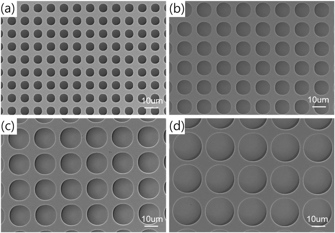 | ||
| Fig. 3 SEM images of patterned holes. (a) Holes with a diameter of 5 μm, (b) 10 μm, (c) 15 μm, and (d) 20 μm are shown. The distance between patterns is 5 μm, and the depth of all holes is 10 μm. All scale bars are 10 μm. | ||
The optimal electrical conditions for effective trapping of particles were determined by frequency sweeping; it was confirmed that the optimal frequency was 1 MHz. When the voltage was fixed at 20 Vpp and 1 kHz, a small number of particles were captured at the edges of the pattern. However, at 1 MHz, all the particles were captured at the edges. The particles were not stably trapped at 1 kHz as a result of side effects, such as alternating current electro-osmosis (ACEO)43,44 and alternating current electrothermal flow (ACET).45,46 At 1 kHz, these two effects dominate the dielectrophoretic force, causing the particles to be pushed into the spaces between the patterns rather than being pulled to the edge.47 Conversely, at 1 MHz, the dielectrophoretic force dominated both effects, resulting in a stable arrangement of the particles at the edges of the pattern. Consequently, we found that the optimal electrical conditions for effective trapping were 20 Vpp and 1 MHz. However, the results varied depending on the pattern diameter. This was because the strength of the electric field varied according to the diameter of the pattern.
At diameters of 5 and 10 μm, the difference between the edge of the pattern and its adjacent area was not significant, resulting in a weakened dielectrophoretic force on the particles. Therefore, the number of captured particles under these conditions was much lower than that for other diameters. On the other hand, at diameters of 15 and 20 μm, the difference was much more significant such that the particles were subjected to a stronger force than the above conditions and all the particles were captured at the edges of the pattern. Thus, we were able to demonstrate the effect of diameter on dielectrophoretic trapping experimentally and theoretically.
Immobilization is necessary for fabricating SERS-active substrates for molecular detection. This was accomplished by using a two-step method. First, the frequency was reduced from 1 MHz to 1 kHz to fix the particles. The frequency was then reverted to 1 MHz, the voltage was reduced to 3 Vpp, and a 3 DC offset was applied to enhance the binding between the substrate and the particles.48–50 In the first step, the capacitance effect resulted in lower frequencies. At 1 MHz, the period was too short to allow sufficient charge accumulation between the particles and the substrate. However, if the frequency was rapidly reduced, a large amount of charge accumulated within a short time. This led to a strong capacitance effect that could immobilize the particles. In the second step, a positive DC offset was applied given that the particles were negatively charged; therefore, the binding between them was reinforced by the electrical force. Fig. 4 shows that the particles were stably attached when the solution was dried and were observable after peeling off the ITO electrode. The optical images of the immobilization step for the particles reveal differences in clarity depending on the measurement conditions. Fig. 5(a–d) were measured in the presence of liquid as the particles would not remain attached without completing the full immobilization process, when dried. In contrast, Fig. 5(e–h) were measured in a dried state, resulting in sharper images due to the absence of liquid interference.
 | ||
| Fig. 4 Optical images of the particle immobilization step. (a) Represents the trapping step (b) represents the immobilization step using the capacitance effect, while (c) represents the immobilization step using a positive current, measured in a dried state. All scale bars are 10 μm. The following are conditions of each step (a) 20 Vpp, 1 MHz. (b) 20 Vpp, 1 kHz. (c) 3 Vpp, 1 MHz with a +3 V DC offset. | ||
 | ||
| Fig. 5 Optical images of gold nanoparticles trapped along the edges of hole patterns. (a–d) Substrates before the immobilization step with hole pattern diameters of 5, 10, 15, and 20 μm, respectively. The images were obtained using a covered, transparent ITO electrode. (e–h) Substrates after the immobilization step with diameters of 5, 10, 15, and 20 μm, respectively, measured in a dried state. All scale bars are 10 μm. | ||
To verify the performance of the fabricated substrates as a molecular detection platform, we measured the SERS signals as 633 nm with different concentrations of Malachite green isothiocyanate (MGITC). The signal was measured down to 10−10 M, and the correlation coefficient (R2) of the calibration curve at 1613 cm−1, which is the signature peak of MGITC, was 0.9611; the results are shown in Fig. 6(c). Raman spectroscopy spectra obtained with other wavelengths are presented in Fig. S5(a).† The enhancement factor (EF) was calculated using the known number of adsorbed molecules and the measured Raman intensity data from our experiments.51,52 As a result, the EF obtained in this study was 2.877 × 10⁷. The detailed calculation procedure is provided in the ESI.†
 | ||
| Fig. 6 (a) Comparison of SERS spectra at following substrates. (1) Is a substrate arranged in a pattern using DEP, (2) is a substrate with random gold particles on a gold substrate, (3) is a substrate with random gold particles on a Si wafer, and (4) is a gold substrate without gold particles. The substrates schematic is shown in Fig. S5(b)† as sample (1–4). (b) SERS spectra at different concentrations (10−5–10−10 M) using a 633 nm laser. (c) Intensity of the Raman spectrum corresponding to the 1613 cm−1 band. The Raman signals were obtained using the average values from 10 different points. The regression equation and R2 value are shown in the graph, where y represents the intensity (Raman counts), and x is the analyte concentration. | ||
In conclusion, in the development of sensitive SERS-based sensors for molecular detection, it is crucial to create consistent hotspots to obtain reliable and reproducible signals. In this study, we performed dielectrophoretic trapping and immobilization of nanoparticles to achieve this objective. The fabricated substrates exhibited uniform high-intensity signals, as validated by comparing its SERS spectra with those of different substrates. Notably, the substrates demonstrated the ability to detect molecules at low concentrations, with sensitivity down to 10−10 M. Consequently, SERS-active substrates fabricated through a dielectrophoretic assembly are expected to be used in various fields because of their ability to provide uniform signals over a large area.
Data availability
The authors confirm that the data supporting the findings of this study are available within the article. The authors will supply the relevant data in response to reasonable requests.Author contributions
Yun Su Yeo: writing – review & editing, writing – original draft, software, methodology, investigation, formal analysis, data curation. Jaejun Park: writing – review & editing, writing – original draft, methodology, investigation, formal analysis, data curation. Sunghoon Yoo: methodology, investigation. Dong Hwan Nam: methodology, investigation. Hayoung Kim: methodology, investigation. Tae Jae Lee: methodology, investigation. Gyu Leem: methodology, investigation. Jae-Sung Kwon: conceptualization, supervision, writing – review & editing. Seunghyun Lee: conceptualization, funding acquisition, project administration, resources, supervision, writing – review & editing.Conflicts of interest
There are no conflicts to declare.Acknowledgements
This work was supported by grants from the National Research Foundation of Korea (RS-2024-00339674 and 2022R1F1A1065369) funded by the Ministry of Science and ICT, Republic of Korea; the Technology Innovation Program (20022507 and RS-2024-00424104) funded By the Ministry of Trade, Industry & Energy (MOTIE, Korea); and the GRRC program of Gyeonggi Province (GRRCHanyang2020-B03), Brain Pool program funded by the Ministry of Science and ICT through the National Research Foundation of Korea (2022H1D3A2A01096391).References
- C. Zhang, D. Paria, S. Semancik and I. Barman, Composite-scattering plasmonic nanoprobes for label-free, quantitative biomolecular sensing, Small, 2019, 15, 1901165, DOI:10.1002/smll.201901165.
- M. Moskovits, Surface-enhanced Raman spectroscopy: a brief retrospective, J. Raman Spectrosc., 2005, 36(6–7), 485–496, DOI:10.1002/jrs.1362.
- A. Campion and P. Kambhampati, Surface-enhanced Raman scattering, Chem. Soc. Rev., 1998, 27(4), 241–250, 10.1039/A827241Z.
- J. M. Nam, J.-W. Oh, H. Lee and Y. D. Suh, Plasmonic nanogap-enhanced Raman scattering with nanoparticles, Acc. Chem. Res., 2016, 49, 2746–2755, DOI:10.1021/acs.accounts.6b00409.
- K. Takemura, Surface plasmon resonance (SPR)- and localized SPR (LSPR)-based virus sensing systems: optical vibration of nano- and micro-metallic materials for the development of next-generation virus detection technology, Biosensors, 2021, 11, 250, DOI:10.3390/bios11080250.
- H.-Y. Chen, M.-H. Lin, C.-Y. Wang, Y.-M. Chang and S. Gwo, Large-scale hot spot engineering for quantitative SERS at the single-molecule scale, J. Am. Chem. Soc., 2015, 137, 13698–13705, DOI:10.1021/jacs.5b09111.
- Y.-M. Lee, S.-E. Kim and J.-E. Park, Strong coupling in plasmonic metal nanoparticles, Nano Converg., 2023, 10, 34, DOI:10.1186/s40580-023-00383-5.
- A. Yadav, L. Zhong, J. Sun, L. Jiang, G. J. Cheng and L. Chi, Tunable random lasing behavior in plasmonic nanostructures, Nano Converg., 2017, 4, 1, DOI:10.1186/s40580-016-0095-5.
- Y. Hu, S. Lee, P. Kumar, Q. Nian, W. Wang, J. Irudayaraj and G. J. Cheng, Water flattens graphene wrinkles: laser shock wrapping of graphene onto substrate-supported crystalline plasmonic nanoparticle arrays, Nanoscale, 2015, 7, 19885–19893, 10.1039/C5NR04810A.
- S. Lee, P. Kumar, Y. Hu, G. J. Cheng and J. Irudayaraj, Graphene laminated gold bipyramids as sensitive detection platforms for antibiotic molecules, Chem. Commun., 2015, 51, 15494–15497, 10.1039/C5CC04890G.
- J. Kneipp, H. Kneipp and K. Kneipp, SERS-a single-molecule and nanoscale tool for bioanalytics, Chem. Soc. Rev., 2008, 37, 1052–1060, 10.1039/B708459P.
- S. Lee, M. G. Hahm, R. Vajtai, D. P. Hashim, T. Thurakitseree, A. C. Chipara, P. M. Ajayan and J. H. Hafner, Utilizing 3D SERS active volumes in aligned carbon nanotube scaffold substrates, Adv. Mater., 2012, 24, 5261–5266, DOI:10.1002/adma.201200645.
- S. Lee, U. S. Kadam, A. P. Craig and J. Irudayaraj, In vivo biodetection using surface-enhanced Raman spectroscopy, CRC Press, Taylor and Francis Group, Florida, 2014 Search PubMed.
- N. Hajduková, M. Procházka, J. Štěpánek and M. Špírková, Chemically reduced and laser-ablated gold nanoparticles immobilized to silanized glass plates: preparation, characterization and SERS spectral testing, Colloids Surf., A, 2007, 301, 264–270, DOI:10.1016/j.colsurfa.2006.12.065.
- S. M. Lee, D. H. Nam, D. Lee, S. H. Lim, S. J. Son and S. Lee, Gold nanoparticles deposited on a conical anodic aluminum oxide substrate for improved surface-enhanced Raman scattering, ACS Appl. Nano Mater., 2021, 4, 12905–12912, DOI:10.1021/acsanm.1c02105.
- Y. S. Hu, J. Jeon, T. J. Seok, S. Lee, J. H. Hafner, R. A. Drezek and H. Choo, Enhanced Raman scattering from nanoparticle-decorated nanocone substrates: a practical approach to harness in-plane excitation, ACS Nano, 2010, 4, 5721–5730, DOI:10.1021/nn101352h.
- S. Kim, S. Yoo, D. H. Nam, H. Kim, J. H. Hafner and S. Lee, Monodispersed mesoscopic star-shaped gold particles via silver-ion-assisted multi-directional growth for highly sensitive SERS-active substrates, Nano Converg., 2024, 11, 26, DOI:10.1186/s40580-024-00435-4.
- S. Yoo, D. H. Nam, T. I. Singh, G. Leem and S. Lee, Effect of reducing agents on the synthesis of anisotropic gold nanoparticles, Nano Converg., 2022, 9, 5, DOI:10.1186/s40580-021-00296-1.
- S. Yoo, G. Youn, H. Lee, J.-S. Kwon, Y. Lee and S. Lee, Synthesis of ultra-small gold nanorods: effect of reducing agent on reaction rate control, Bull. Korean Chem. Soc., 2023, 44, 648–652, DOI:10.1002/bkcs.12706.
- S. Eslami and S. Palomba, Integrated enhanced Raman scattering: a review, Nano Converg., 2021, 8(1), 41, DOI:10.1186/s40580-021-00290-7.
- N. A. Hatab, C.-H. Hsueh, A. L. Gaddis, S. T. Retterer, J.-H. Li, G. Eres, Z. Zhang and B. Gu, Free-standing optical gold bowtie nanoantenna with variable gap size for enhanced Raman spectroscopy, Nano Lett., 2010, 10, 4952–4955, DOI:10.1021/nl102963g.
- A. M. Jubb, Y. Jiao, G. Eres, S. T. Retterer and B. Gu, Elevated gold ellipse nanoantenna dimers as sensitive and tunable surface enhanced Raman spectroscopy substrates, Nanoscale, 2016, 8, 5641–5648, 10.1039/C5NR08920D.
- Z. Zhang, Y. Lee, M. F. Haque, J. Leem, E. Y. Hsieh and S. W. Nam, Plasmonic sensors based on graphene and graphene hybrid materials, Nano Converg., 2022, 9, 28, DOI:10.1186/s40580-022-00319-5.
- A. Das, K. Kim, S.-G. Park, N. Choi and J. Choo, SERS-based serodiagnosis of acute febrile diseases using plasmonic nanopopcorn microarray platforms, Biosens. Bioelectron., 2021, 192, 113525, DOI:10.1016/j.bios.2021.113525.
- M. A. M. Ali, A. B. A. Kayani and B. Y. Majlis, Biological particle control and separation using active forces in microfluidic environments, Microfluidics and Nanofluidics, ed. Kandelousi, InTech, 2018 Search PubMed.
- O. Péron, E. Rinnert, M. Lehaitre, P. Crassous and C. Compère, Detection of polycyclic aromatic hydrocarbon (PAH) compounds in artificial sea-water using surface-enhanced Raman scattering (SERS), Talanta, 2009, 79, 199–204, DOI:10.1016/j.talanta.2009.03.043.
- P. Reineck, C. J. Wienken and D. Braun, Thermophoresis of single stranded DNA, Electrophoresis, 2010, 31, 279–286, DOI:10.1002/elps.200900505.
- H. Lee, D. Hong, H. Cho, J. Y. Kim, J. H. Park, S. H. Lee, H. M. Kim, R. F. Fakhrullin and I. S. Choi, Turning diamagnetic microbes into multinary micro-magnets: magnetophoresis and spatio-temporal manipulation of individual living cells, Sci. Rep., 2016, 6, 38517, DOI:10.1038/srep38517.
- X. Jin, S. Abbot, X. Zhang, L. Kang, V. Voskinarian-Berse and R. Zhao, et al., Erythrocyte enrichment in hematopoietic progenitor cell cultures based on magnetic susceptibility of the hemoglobin, PLoS One, 2012, 7, e39491, DOI:10.1371/journal.pone.0039491.
- H. A. Pohl, Dielectrophoresis: the behavior of neutral matter in nonuniform electric fields, Cambridge University Press, Cambridge, 1978 Search PubMed.
- K. M. Mayer, S. Lee, H. Liao, B. C. Rostro, A. Fuentes, P. T. Scully, C. L. Nehl and J. H. Hafner, A label-free immunoassay based upon localized surface plasmon resonance of gold nanorods, ACS Nano, 2008, 2, 687–692, DOI:10.1021/nn7003734.
- S. Lee, K. M. Mayer and J. H. Hafner, Improved localized surface plasmon resonance immunoassay with gold bipyramid substrates, Anal. Chem., 2009, 81, 4450–4455, DOI:10.1021/ac900276n.
- N. Abd Rahman, F. Ibrahim and B. Yafouz, Dielectrophoresis for biomedical sciences applications: a review, Sensors, 2017, 17, 449, DOI:10.3390/s17030449.
- N. G. Green, A. Ramos and H. Morgan, Numerical solution of the dielectrophoretic and travelling wave forces for interdigitated electrode arrays using the finite element method, J Electrostat., 2002, 56, 235–254, DOI:10.1016/S0304-3886(02)00069-4.
- A. Yamaguchi, Y. Utsumi and T. Fukuoka, Aggregation and dispersion of Au-nanoparticle-decorated polystyrene beads with SERS-activity using AC electric field and Brownian movement, Appl. Surf. Sci., 2019, 465, 405–412, DOI:10.1021/j100368a049.
- H. Morgan and N. G. Green, AC electrokinetics: colloids and nanoparticles, Research Studies Press, Baldock, 2003, DOI:10.1007/978-94-007-6178-0_130-2.
- B. C. Gierhart, D. G. Howitt, S. J. Chen, R. L. Smith and S. D. Collins, Frequency dependence of gold nanoparticle superassembly by dielectrophoresis, Langmuir, 2007, 23, 12450–12456, DOI:10.1021/la701472y.
- N. G. Green, Dielectrophoresis and AC electrokinetics, in Electrokinetics and Electrohydrodynamics in Microsystems, Springer Vienna, Vienna, 2011, pp. 61–84, DOI:10.1007/978-3-7091-0900-7.
- C. Yang, C.-J. Wu, A. E. Ostafin, G. Thibaudeau and A. R. Minerick, Size and medium conductivity dependence on dielectrophoretic behaviors of gas core poly-l-lysine shell nanoparticles, Electrophoresis, 2015, 36, 1002–1010, DOI:10.1002/elps.201400315.
- C. K. Dixit, S. Bhakta, A. Kumar, S. L. Suib and J. F. Rusling, Fast nucleation for silica nanoparticle synthesis using a sol–gel method, Nanoscale, 2016, 8, 19662–19667, 10.1039/C6NR07568A.
- T. Pham, J. B. Jackson, N. J. Halas and T. R. Lee, Preparation and characterization of gold nanoshells coated with self-assembled monolayers, Langmuir, 2002, 18, 4915–4920, DOI:10.1021/la015561y.
- S. J. Oldenburg, R. D. Averitt, S. L. Westcott and N. J. Halas, Nanoengineering of optical resonances, Chem. Phys. Lett., 1998, 288, 243–247, DOI:10.1016/S0009-2614(98)00277-2.
- M. Z. Bazant and Y. Ben, Theoretical prediction of fast 3D AC electro-osmotic pumps, Lab Chip, 2006, 6, 1455–1461, 10.1039/B608092H.
- B. Weiss, W. Hilber, P. Gittler and B. Jakoby, Particle separation in alternating-current electro-osmotic micropumps using field-flow fractionation, Microfluid. Nanofluid., 2009, 7, 191–203, DOI:10.1063/1.2918129.
- S. Dash and S. Mohanty, Dielectrophoretic separation of micron and submicron particles: a review, Electrophoresis, 2014, 35, 2656–2672, DOI:10.1002/elps.201400084.
- A. Salari, M. Navi, T. Lijnse and C. Dalton, AC electrothermal effect in microfluidics: a review, Micromachines, 2019, 10, 762, DOI:10.3390/mi10110762.
- D. F. Chen, H. Du and W. H. Li, Bioparticle separation and manipulation using dielectrophoresis, Sens. Actuators, A, 2007, 133, 329–334, DOI:10.1016/j.sna.2006.06.029.
- R. Kataoka, H. Tokita, S. Uchida, R. Sano and H. Nishikawa, Frequency dependence and assembly characteristics of silver nanomaterials trapped by dielectrophoresis, J. Phys.: Conf. Ser., 2015, 646, 012005, DOI:10.1088/1742-6596/646/1/012005.
- M. Hakoda, Development of dielectrophoresis separator with an insulating porous membrane using DC-offset AC electric fields, Biotechnol. Prog., 2016, 32, 1292–1300, DOI:10.1002/btpr.2330.
- Y. J. Eo, G. Y. Yoo, H. Kang, Y. K. Lee, C. S. Kim, J. H. Oh, K. N. Lee, W. Kim and Y. R. Do, Enhanced DC-operated electroluminescence of forwardly aligned p/MQW/n InGaN nanorod LEDs via DC offset-AC dielectrophoresis, ACS Appl. Mater. Interfaces, 2017, 9, 37912–37920, DOI:10.1021/acsami.7b09794.
- S. Cherukulappurath, S. H. Lee, A. Campos, C. L. Haynes and S. H. Oh, Rapid and sensitive in situ SERS detection using dielectrophoresis, Chem. Mater., 2014, 26(7), 2445–2452, DOI:10.1021/cm500062b.
- L. O. Brown and S. K. Doorn, Optimization of the preparation of glass-coated, dye-tagged metal nanoparticles as SERS substrates, Langmuir, 2008, 24(5), 2178–2185, DOI:10.1021/la703218f.
Footnotes |
| † Electronic supplementary information (ESI) available. See DOI: https://doi.org/10.1039/d5lc00238a |
| ‡ These authors contributed equally to this work. |
| This journal is © The Royal Society of Chemistry 2025 |