
 Open Access Article
 This Open Access Article is licensed under a
 Creative Commons Attribution 3.0 Unported Licence
Enhanced bending stability of flexible perovskite solar cells on stainless steel substrates via C60 buffer layer integration†
Hyun Jeong
Lee‡
 a,
Kyunghwan
Kim‡
b,
Solhee
Lee
b,
Dowon
Pyun
b,
Ji-Seong
Hwang
b,
Jiyeon
Nam
b,
Sujin
Cho
b,
Seok-Hyun
Jeong
b,
Donghwan
Kim
b,
Yoonmook
Kang
cd,
Dong Ha
Kim
*aefgh and
Hae-Seok
Lee
*cd
a,
Kyunghwan
Kim‡
b,
Solhee
Lee
b,
Dowon
Pyun
b,
Ji-Seong
Hwang
b,
Jiyeon
Nam
b,
Sujin
Cho
b,
Seok-Hyun
Jeong
b,
Donghwan
Kim
b,
Yoonmook
Kang
cd,
Dong Ha
Kim
*aefgh and
Hae-Seok
Lee
*cd
aDepartment of Chemistry and Nanoscience, Ewha Womans University, 52, Ewhayeodae-gil, Seodaemun-gu, Seoul 03760, Republic of Korea. E-mail: dhkim@ewha.ac.kr
bDepartment of Materials and Engineering, Korea University, Seoul 02841, Republic of Korea
cGraduate School of Energy and Environment (KU-KIST Green School), Korea University, Seoul 02841, Republic of Korea. E-mail: lhseok@korea.ac.kr
dDepartment of Integrative Energy Engineering, Korea University, Seoul 02841, Republic of Korea
eCollege of Medicine, Ewha Womans University, 25, Magokdong-ro 2-gil, Gangseo-gu, Seoul 07804, Republic of Korea
fGradutate Program in Innovative Biomaterials Convergence, Ewha Womans University, 52 Ewhayeodae-gil, Seodaemun-gu, Seoul 03760, Republic of Korea
gBasic Sciences Research Institute (Priority Research Institute), Ewha Womans University, 52, Ewhayeodae-gil, Seodaemun-gu, Seoul 03760, Republic of Korea
hNanobio Energy Materials Center (National Research Facilities and Equipment Center), Ewha Womans University, 52, Ewhayeodae-gil, Seodaemun-gu, Seoul 03760, Republic of Korea
First published on 14th July 2025
Abstract
Flexible perovskite solar cells (PSCs) based on stainless steel (SS) substrates offer a highly promising platform for next-generation Building-Integrated Photovoltaics (BIPV) and Vehicle-Integrated Photovoltaics (VIPV), owing to their superior durability, mechanical strength, and thermal resilience. However, achieving long-term operational stability under bending stress remains a significant hurdle. In this work, we identify fractures in the TiO2 electron transport layer as the dominant source of performance degradation under mechanical deformation. To address this issue, we introduce a C60 buffer layer atop the TiO2, which serves dual functions: mechanical protection and enhanced interfacial charge extraction. The C60 layer functions by redistributing strain through a shift of the neutral axis closer to the TiO2 layer and by passivating interfacial trap states, as confirmed by SEM, AFM, PL, TRPL, and EIS analyses. As a result, SS-based PSCs with an optimized 20 nm C60 layer demonstrate a remarkable ∼5% increase in PCE before bending and an ∼92.84% improvement in PCE retention after bending, compared to control devices. Furthermore, devices maintained superior performance over 100 bending cycles and continuous bending for 100 hours. These findings establish the C60 buffer layer as a powerful strategy for enabling flexible PSCs with both high efficiency and mechanical reliability, accelerating their practical deployment in BIPV and VIPV systems where mechanical stress is unavoidable.
Broader contextFlexible and durable perovskite solar cells (PSCs) are essential for emerging applications in building-integrated photovoltaics (BIPV) and vehicle-integrated photovoltaics (VIPV). This study addresses the mechanical and electrical challenges faced by stainless steel (SS)-based PSCs under bending conditions and proposes a strategy to enhance their stability and efficiency. By incorporating a 20 nm thick C60 buffer layer, we significantly improved bending durability and charge extraction efficiency, mitigating damage to the TiO2 layer. The optimized SS-based PSCs achieved a 92.84% improvement in PCE retention after bending, demonstrating the potential of C60 integration as a viable approach for robust and flexible PSCs. These findings contribute to the advancement of high-performance, flexible photovoltaics for next-generation energy applications. |
Introduction
Recent years have witnessed substantial progress in the development of flexible solar cells tailored for Building-Integrated Photovoltaics (BIPV) and Vehicle-Integrated Photovoltaics (VIPV).1–4 Among these advancements, stainless steel (SS)-based perovskite solar cells (PSCs) have garnered significant attention due to their remarkable durability, superior mechanical strength, and flexibility, which surpass those of conventional flexible substrates.5–8 These attributes render SS-based PSCs highly suitable for demanding applications in BIPV and VIPV, where structural stability under mechanical stress is essential.9–12 Despite these advantages, SS-based PSCs continue to face critical challenges, particularly efficiency degradation when subjected to bending and mechanical stress. While SS-based PSCs have emerged as a promising alternative to overcome these limitations, the majority of research to date has remained focused on polymer-based substrates, such as polyethylene terephthalate (PET) and polyethylene naphthalate (PEN).13–16 Li et al. reported a flexible PSCs incorporating a bioinspired multisite polymer, which achieved a power conversion efficiency (PCE) of 24.43% and retained 94.1% of its initial performance after 10![[thin space (1/6-em)]](https://www.rsc.org/images/entities/char_2009.gif) 000 bending cycles under high humidity conditions.17 Similarly, Chalkias et al. demonstrated a carbon-based flexible PSCs fabricated under ambient air, achieving a PCE of 20.09% and maintaining mechanical stability over 5000 bending cycles.18 Furthermore, Dong et al. developed a fully printed flexible PSCs module that preserved 95% of its original efficiency after 3000 cycles of mechanical deformation.19 These studies collectively highlight key strategies to simultaneously enhance efficiency and mechanical robustness, including the introduction of elastic or ductile interlayers, surface modifications to improve interfacial adhesion and stress distribution, and structural designs that position functional layers near the neutral mechanical plane.
000 bending cycles under high humidity conditions.17 Similarly, Chalkias et al. demonstrated a carbon-based flexible PSCs fabricated under ambient air, achieving a PCE of 20.09% and maintaining mechanical stability over 5000 bending cycles.18 Furthermore, Dong et al. developed a fully printed flexible PSCs module that preserved 95% of its original efficiency after 3000 cycles of mechanical deformation.19 These studies collectively highlight key strategies to simultaneously enhance efficiency and mechanical robustness, including the introduction of elastic or ductile interlayers, surface modifications to improve interfacial adhesion and stress distribution, and structural designs that position functional layers near the neutral mechanical plane.
In environments such as construction and automotive applications, solar cells are frequently exposed to a range of stressors, including temperature fluctuations, physical impacts, prolonged moisture, and ultraviolet (UV) radiation.20 The inherent mechanical strength of stainless steel offers a robust foundation capable of withstanding bending and deformation, ensuring the structural and functional stability of PSCs under such adverse conditions. Research into SS-based PSCs has shown considerable progress in recent years. For instance, in 2022, Feleki et al. achieved a PCE of 16.5% in p–i–n structured SS-based PSCs fabricated on polymer-coated SS substrates.5 Zheng et al. improved the PCE to 17.1% in 2023 by introducing an 80 nm indium tin oxide (ITO) interlayer and applying surface passivation techniques.7 In 2024, Zhou et al. further enhanced SS-based PSC performance, achieving a PCE of 20.2% by incorporating single crystals into the precursor solution to reduce perovskite defects and passivating the surface of the perovskite film.8
Despite these advancements, efficiency degradation under mechanical stress remains a persistent challenge for SS-based PSCs. Bending and deformation can lead to micro-crack formation, delamination within the functional layers, and hindered charge transport, ultimately resulting in power loss.21,22 Moreover, mechanical stress exacerbates ion migration and layer instability within the perovskite material, further reducing operational efficiency. Therefore, improving the mechanical and operational stability of SS-based PSCs under bending conditions remains a pivotal research focus. While significant progress has been made in advancing SS-based PSCs, there is a notable gap in understanding the specific causes of efficiency degradation under bending conditions. Investigating these mechanisms is essential for enabling the practical application of SS-based PSCs in BIPV and VIPV, where mechanical robustness and long-term performance are critical.
In this work, we address the key mechanical limitations of SS-based PSCs, which are highly promising for real-world flexible photovoltaic applications. We identify the fracture of the TiO2 electron transport layer as a critical factor contributing to performance degradation under bending conditions and propose the integration of a C60 buffer layer as a dual-function solution that provides both mechanical stress relief and enhanced interfacial charge extraction. Unlike conventional approaches that focus solely on either flexibility or efficiency, our strategy simultaneously enhances both mechanical robustness and electronic performance. This study presents a novel design principle for realizing high-efficiency, mechanically stable SS-based PSCs, paving the way for their practical implementation in BIPV and VIPV. Notably, the optimized device incorporating a 20 nm C60 buffer layer exhibited a PCE of 17.51% before bending and retained approximately 92.84% of its initial performance after bending.
Results and discussion
To explore the causes of efficiency degradation in SS-based PSCs, scanning electron microscopy (SEM) measurements were performed to observe structural changes induced by bending. The samples were subjected to a bending diameter of 10 mm for 1 hour prior to analysis. Fig. 1a and c present schematic representations of surface damage phenomena observed without and with the incorporation of a C60 buffer layer, respectively. As depicted in Fig. 1b, the TiO2 layer exhibits a smooth surface prior to bending, while clear fractures appear after bending. Conversely, when a C60 buffer layer is incorporated, as shown in Fig. 1d, the TiO2 layer remains intact, exhibiting no fractures even after bending. In addition, atomic force microscopy (AFM) measurements were conducted to evaluate surface roughness. The TiO2 film displayed roughness values of 49 nm before bending and 144 nm after bending, indicating significant surface damage due to bending (Fig. S1a and S1c, ESI†). In contrast, the C60/TiO2 hybrid film showed roughness values of 15 nm before bending and 44 nm after bending, maintaining a significantly smoother surface compared to the single TiO2 film (Fig. S1b and S1d, ESI†). Although both films displayed a similar relative increase in roughness, the absolute roughness of the C60/TiO2 film remained significantly lower. It should be noted, however, that the AFM measurements represent localized surface characteristics and may not comprehensively reflect the overall stress distribution within the complete multilayered device under bending conditions. Therefore, the roughness data are used here as supportive indicators of morphological trends rather than as definitive predictors of mechanical failure. Further analysis of the indium tin oxide thin film using the same methodology revealed no fractures in the ITO layer after bending (Fig. S2, ESI†). These results indicate that preventing fractures in the TiO2 layer is crucial for enhancing the efficiency and mechanical stability of SS-based PSCs. | ||
| Fig. 1 Surface damage assessment of TiO2 due to bending: (a) schematic illustration showing the surface damage of TiO2 after bending. (c) Schematic illustration of C60/TiO2 deposited on SS-based PSCs after bending. (b) SEM images of TiO2 before and after bending. (d) SEM images of C60/TiO2 deposited on SS-based PSCs before and after bending. (e) Schematic illustration of the neutral axis shifts in SS-based PSCs without and with the C60 buffer layer. | ||
The changes experienced by each layer in multilayered structures before and after bending are illustrated in Fig. S3, ESI.† In this analysis, y represents the distance from the neutral axis, R denotes the radius relative to the neutral axis, and θ indicates the central angle with respect to the neutral axis. When bending is applied, each layer undergoes stress (σ)—the force exerted to maintain its shape against external forces—and strain (ε), the deformation resulting from these forces.23–27 Specifically, layers above the neutral axis experience tensile forces, while layers below it are subjected to compressive forces. According to the stress–strain behaviour of ceramic materials, exceeding a certain stress threshold causes the material to lose its ability to return to its original state, ultimately leading to failure.28 The relationships between ε and σ in the layers during bending are described by the equations shown in Fig. 1e.21,29,30
 | (1) |
 | (2) |
While eqn (1) and (2) provide a fundamental analytical framework for evaluating strain and stress distributions in multilayer structures, they are based on idealized assumptions, including uniform Young's modulus and linear elastic behavior. Notably, the Young's modulus values used in the analysis are derived from bulk materials reported in the literature and may not accurately reflect the mechanical response of nanostructured thin films under bending deformation. As such, the results should be interpreted qualitatively, emphasizing relative trends rather than absolute values.
When a C60 layer is introduced on top of the TiO2 layer, the neutral axis (N) of the layered structure is theoretically expected to shift slightly. The position of the neutral axis can be estimated using eqn (3), assuming ideal layer homogeneity and isotropy:21,31
 | (3) |
To fabricate SS-based PSCs with a C60 buffer layer, the effects of C60 on the perovskite crystal structure were investigated. Fig. 2a shows the SS304 substrate and the chemical structure of C60 used as the buffer layer in this study. To investigate molecular interactions between perovskite and C60, X-ray photoelectron spectroscopy (XPS) was conducted. In Fig. 2b, the binding energy peaks of I 3d5/2 and I 3d3/2 in the MAPbI3 film appear at 618.68 eV and 630.18 eV, respectively. For the MAPbI3/C60 composite layer, these peaks shift to lower values by 0.4 eV and 0.2 eV, respectively, indicating strong electronic interactions between C60 and I− ions due to charge transfer.32,33 Similarly, Fig. 2e shows that the binding energy peaks of Pb 4f7/2 and Pb 4f5/2 in the MAPbI3 film, originally at 136.98 eV and 141.88 eV, shift to lower values by 0.3 eV and 0.4 eV, respectively, in the MAPbI3/C60 composite structure. This negative shift indicates strong interactions between C60 and Pb2+ ions, which contribute to defect passivation and enhanced interfacial charge transfer.32 The crystallization of perovskite on the SS substrate was analyzed using X-ray diffraction (XRD), as shown in Fig. 2d. MAPbI3/C60/TiO2 films and MAPbI3/TiO2 films were prepared on SS substrates via the same deposition process. Both samples exhibit distinct diffraction peaks at 14.11° and 28.45°, corresponding to the (110) and (220) planes of MAPbI3, respectively.34,35 The similarity in diffraction intensity between MAPbI3/C60/TiO2 and MAPbI3/TiO2 indicates that the incorporation of C60 does not alter the crystallinity of the perovskite, confirming that a highly crystalline MAPbI3 thin film can be formed on the SS substrate even in the presence of C60. Charge extraction properties were further analyzed using steady-state photoluminescence (PL) and time-resolved photoluminescence (TRPL) measurements. Fig. 2e shows that all samples exhibit a PL peak at 770 nm, originating from MAPbI3. The PL quantum yield significantly decreases with the incorporation of TiO2 and C60, demonstrating efficient charge carrier extraction from MAPbI3 to C60.36,37 The most pronounced PL quenching observed in the MAPbI3/C60/TiO2 structure indicates superior carrier extraction facilitated by C60.38 TRPL decay curves for MAPbI3, MAPbI3/TiO2, and MAPbI3/C60/TiO2 samples are shown in Fig. 2f, with detailed lifetime values provided in Table S2.† For the MAPbI3 sample, the fast lifetime (τ1) and average lifetime (τave) were calculated as 14.09 ns and 66.30 ns, respectively. With the introduction of the C60 buffer layer, these values decreased to 8.24 ns and 52.34 ns, respectively, indicating faster PL quenching and higher electron injection efficiency, ultimately enhancing photovoltaic performance.39
 | ||
| Fig. 2 Assessment of C60 characteristics and suitability as an interlayer: (a) image of SS substrate (left) and chemical structure of the C60 (right). (b) XPS spectra showing the I 3d peaks for MAPbI3/TiO2 and MAPbI3/C60/TiO2 hybrid films. (c) XPS spectra showing the Pb 4f peaks for perovskite/TiO2 and MAPbI3/C60/TiO2 hybrid films. (d) XRD patterns of the MAPbI3/TiO2 and MAPbI3/C60/TiO2 hybrid films. (e) Steady-state PL spectra and (f) time-resolved PL decay spectra of MAPbI3/TiO2 and MAPbI3/C60/TiO2 hybrid films. | ||
Fig. 3a shows the schematic of the fabricated SS-substrate-based PSC. The corresponding SEM cross-sectional image of the device is shown in Fig. 3b. The fabrication process of the device is illustrated in Fig. S4, ESI.† Due to the opaque nature of the SS substrate, light illumination was applied from the top side of the device. To enable this, a transparent ITO electrode was deposited on the top surface, followed by patterned Au deposition that served as the charge-collecting electrode while allowing light to pass through the ITO openings. This top-illumination configuration ensures accurate photovoltaic characterization of the SS-based PSCs (Fig. S5, ESI†). Fig. 3c shows the energy level diagram of the SS-based PSC, where the C60 buffer layer efficiently extracts photogenerated electrons from the perovskite to the TiO2 layer. This highlights the role of C60 in facilitating charge separation and enhancing photovoltaic performance. To optimize C60 thickness, devices with varying C60 layers (5 nm, 10 nm, 20 nm, and 30 nm) were fabricated and measured under AM 1.5G illumination at 100 mW cm−2 (1 sun). The perovskite crystal structure remained unaffected by C60 variation (Fig. S6, ESI†). At 5 nm, the device achieved an open-circuit voltage (Voc) of 1.00 V, a short-circuit current density (Jsc) of 21.48 mA cm−2, a fill factor (FF) of 68.90, and a power conversion efficiency of 14.83% (Fig. S7a, ESI†). At 10 nm, the device showed a slightly improved PCE of 16.07%, while Voc, Jsc, and FF remained nearly unchanged (Fig. S7b, ESI†). The highest performance was achieved at 20 nm with a Voc of 1.03 V, a Jsc of 20.46 mA cm−2, an FF of 82.52, and a peak PCE of 17.51% (Fig. 3d). At 30 nm, the PCE dropped to 14.75% due to a decrease in FF to 74.60 (Fig. S7c, ESI†). EQE spectra (Fig. S8, ESI†) confirmed that performance improved with increasing C60 thickness up to 20 nm, but declined at 30 nm. Devices with thinner C60 layers (5 nm and 10 nm) exhibited incomplete surface coverage on ITO, limiting performance. In contrast, the 20 nm C60 layer achieved better surface coverage, improved charge extraction and overall efficiency. At 30 nm, the thicker C60 layer partially absorbed sunlight, which reduced carrier generation and lowered performance.40 These results indicate that 20 nm is optimal for C60 thickness. Fig. 3d shows J–V curves comparing devices with and without 20 nm C60. The champion device achieved a high PCE of 17.51%, a Voc of 1.03 V, a Jsc of 20.46 mA cm−2, and an FF of 82.52, significantly outperforming the device without the C60 layer, which exhibited a PCE of 13.86%, a Voc of 0.92 V, a Jsc of 19.29 mA cm−2, and an FF of 88.00. The 20 nm C60 layer improved PCE by ∼4%. To evaluate the hysteresis behavior of the devices, forward and reverse J–V scans were performed before bending. The device without the C60 exhibited significant hysteresis, as evidenced by the large discrepancy between forward (dashed) and reverse (solid) scans. In contrast, the C60-buffered device showed a markedly reduced hysteresis, indicating improved interfacial charge extraction and suppressed ion migration at the TiO2/perovskite interface. Fig. 3e illustrates the EQE spectra in the wavelength range of 400–800 nm, showing higher EQE values for C60-incorporated devices. Box plots in Fig. 3f–i summarize performance data from 16 devices with and without C60. The 20 nm C60 layer slightly improved and stabilized Voc and Jsc, due to reduced interfacial recombination and enhanced charge transport.41 These trends align with PL spectra results (Fig. 2g). The most notable improvement was in PCE, mainly from stabilized FF along with slight Voc and Jsc increases. These results confirm that C60 improves both the interfacial quality and the overall photovoltaic performance.42 To investigate the reasons behind the improved photovoltaic performance, SEM measurements were conducted (Fig. S9, ESI†). Perovskite grains grown on the C60/TiO2 composite layer were significantly larger than those grown directly on the TiO2 substrate. This is attributed to the C60 buffer layer, which lowers interfacial energy between TiO2 and the perovskite precursor solution. This reduction in interfacial energy improves wetting properties during the crystallization process, facilitating the formation of larger grains. Furthermore, the C60 layer mitigates the surface roughness and defects of the TiO2 substrate, providing a smoother surface that promotes unobstructed grain growth.43 Additionally, the fullerene-based C60 buffer layer serves as a passivation layer, effectively suppressing interfacial trap states44,45 Besides electron transport, the C60 layer passivated interfacial trap states and blocked I− ion migration, suppressing PbI2 formation from reactions between I− and TiO2 oxygen vacancies.46
 | ||
| Fig. 3 Characterization and performance of SS-based PSCs: (a) schematic illustration of SS-based PSCs. (b) Cross-sectional SEM image of SS-based PSCs. (c) Energy level diagram of SS-based PSCs. (d) J–V characteristics of the most efficient devices with and without the C60 layer (solid: reverse, dash: forward). (e) EQE plots of devices with and without the C60 layer. (f–i) Statistical deviation of the photovoltaic parameters of the SS-based PSCs with and without the C60 layer in the reverse scanning direction. (The error bar represents standard deviation from 16 devices). | ||
To evaluate the potential application of C60-incorporated SS-based PSCs in BIPV and VIPV systems, the efficiency change under bending conditions was analyzed. Fig. 4a presents a schematic diagram of the fabricated SS-based PSCs, while Fig. 4b (left image) shows the fabricated SS-based PSCs and the right image illustrates the cell bent to a diameter of 10 mm. As shown in Fig. 4c, the SS-based PSC without C60 incorporation, bent to a diameter of 10 mm, exhibited a Voc of 0.77 V, a Jsc of 17.20 mA cm−2, a FF of 50.00, and a PCE of 6.70%. Compared to the unbent condition, the PCE decreased by approximately 7.16% after bending, indicating that the device is unsuitable for applications requiring various curved forms, such as those in BIPV and VIPV systems. In contrast, as shown in Fig. 4b, the C60-incorporated SS-based PSCs, bent to a diameter of 10 mm, achieved a Voc of 1.01 V, a Jsc of 17.82 mA cm−2, a FF of 71.69, and a PCE of 12.92%. Compared to the unbent condition, the PCE exhibited a reduction of only 4.59%, which is significantly lower than the 7.16% reduction observed in devices without C60 incorporation. Moreover, the PCE improved by 6.22% compared to devices prior to the introduction of C60. After bending, the difference in hysteresis became even more pronounced. As shown in Fig. 4c, the device without the C60 buffer layer exhibited aggravated hysteresis behavior due to mechanical damage in the TiO2 layer, whereas the device incorporating the C60 buffer layer maintained superior mechanical and electrical stability. Fig. 4d illustrates the EQE values of cells with and without C60 incorporation after bending to a diameter of 10 mm. It is evident that the EQE values of the cells without C60 are significantly lower than those of the cells with C60. This finding suggests that C60 not only enhances charge extraction through surface modification but also partially prevents degradation of the TiO2 layer during bending. Fig. 4e–h show box plots comparing the Voc, Jsc, FF, and PCE values of 16 SS-based PSCs with and without C60 incorporation after bending to a diameter of 10 mm. When a 20 nm thick C60 layer was incorporated into SS-based PSCs, post-bending performance significantly improved compared to devices without the C60 layer. While the FF showed a slight increase, noticeable enhancements were observed in the Voc, Jsc, and PCE. This improvement is attributed to the ability of C60 to reduce defects at the TiO2 interface, suppress interfacial recombination, and mitigate structural damage to the TiO2 layer during bending. These properties allow the device to maintain high performance under mechanical stress. The incorporation of C60 demonstrates significant potential for enabling the application of SS-based PSCs in BIPV and VIPV systems. The performance of previously reported SS-based PSCs has been summarized in Table S3, ESI.†
 | ||
| Fig. 4 Performance of SS-based flexible PSCs after bending: (a) schematic illustration of the SS-based flexible PSCs. (b) Images of SS-based flexible PSCs before and after bending. (c) J–V characteristics of the most efficient devices after bending with and without the C60 layer (solid: reverse, dash: forward). (d) EQE plots of devices after bending with and without the C60 layer. (e–h) Statistical deviation of photovoltaic parameters of the SS-based PSCs after bending with and without the C60 layer in the reverse scanning direction. (The error bar represents standard deviation from 16 devices). | ||
To understand why the incorporation of C60 prevents performance degradation in SS-based PSCs after bending, the stress concentration factor (K) was analyzed.47K quantifies the concentration of stress due to load transfer obstruction at specific points, such as notches and tips. The value of K is governed by the following equation:48,49
 | (4) |
 | (5) |
 | ||
| Fig. 5 Structural and electrical properties before and after bending: AFM 3D image of the device before and after bending (a) without (before RMS: 49.44 nm, Ra: 87.37 nm, Rp: 677.40 nm) (after RMS: 144.21 nm, Ra: 130.83 nm, Rp: 818.20 nm) (height range: −500 to +500 nm) and (b) with (before RMS: 15.92 nm, Ra: 10.71 nm, Rp: 293.00 nm) (after RMS: 44.23 nm, Ra: 30.02 nm, Rp: 386.90 nm) (height range: −300 to +300 nm) C60. C-AFM image of the device after bending (c) without (min: 0.02 nA, max: 6.72 nA, mean: 2.38 nA) and (d) with (min: 0.19 nA, max: 10.43 nA, mean: 6.54 nA) C60. Nyquist plot of SS-based PSCs without and with C60 (e) before and (f) after bending. | ||
To evaluate the impact of TiO2 substrate fracture on conductivity, C-AFM measurements were conducted. Fig. 5c presents the results for the device without C60 after bending. The dark regions represent non-conductive areas, while the bright regions indicate conductive areas.50,51 The film without C60 exhibited an average current level of 2.38 nA. In contrast, when C60 was incorporated, the film displayed significantly higher conductivity, as shown in Fig. 5d.52,53 The average current level increased to 6.54 nA. This observation aligns with the previously reported efficiency data for SS-based PSCs, demonstrating a similar trend. These findings indicate that the incorporation of C60 effectively reduces stress on the TiO2 layer during bending, contributing to the maintenance of the device's efficiency under mechanical stress. To further investigate the effects of the C60 layer on charge extraction and device stability under bending conditions, electrochemical impedance spectroscopy (EIS) measurements were performed. The Nyquist plots in Fig. 5e compare the EIS data of devices with and without the C60 layer before bending. The device with C60 exhibits a significantly smaller semicircle in the high-frequency region, indicating a reduced charge transfer resistance (Rtrans). This improvement is attributed to the C60 layer's ability to enhance charge extraction at the MAPbI3/TiO2 interface by reducing interfacial defects and facilitating efficient electron transport. Furthermore, the semicircle in the low-frequency region, representing recombination resistance (Rrec), is notably larger in the device with C60. The increased Rrec demonstrates effective suppression of charge recombination at the interface, contributing to the enhanced performance of the device.54Fig. 5f illustrates the EIS data for devices with and without the C60 layer after bending. Bending introduces mechanical stress that degrades the TiO2 layer and increases interfacial defects. For the device without C60, Rtrans increases significantly, as evidenced by the enlarged high-frequency semicircle. In contrast, the device with C60 maintains a relatively smaller Rtrans, emphasizing the protective role of C60 in preserving charge transport pathways. Additionally, while the low-frequency semicircle (Rrec) shrinks for both devices due to increased defect density caused by bending, the reduction in Rrec is less pronounced in the device with C60. This indicates that the C60 layer mitigates recombination losses even under mechanical stress. These findings confirm that the incorporation of C60 not only enhances charge extraction efficiency but also provides improved structural stability to the device under bending conditions. These improvements reflect not only reduced surface stress but also enhanced interfacial integrity and defect tolerance enabled by the C60 layer. By reducing stress concentration factors, facilitating efficient electron transport, and suppressing charge recombination, the C60 layer significantly contributes to the mechanical and operational stability of SS-based PSCs.54
To evaluate the morphological and functional stability of C60-incorporated SS-based PSCs under mechanical deformation, PCE measurements were conducted under various static and dynamic bending conditions. Rather than aiming to extract classical mechanical parameters, this experiment was designed to assess the device performance and interface durability under realistic bending stress. Fig. 6a presents the results of PCE measurements as the bending diameter was adjusted from a flat state to a diameter of 5 mm. The PCE degradation rate was significantly lower in devices with C60 incorporation compared to those without, suggesting enhanced tolerance to bending-induced morphological disruption. Fig. 6b displays images of the devices at bending diameters of 12 mm, 9 mm, and 5 mm, illustrating their structural flexibility under increasing mechanical strain. In the second evaluation, dynamic mechanical stress was applied via repeated bending cycles. As shown in Fig. 6c, when the number of bending cycles increased from 0 to 100, devices with C60 incorporation exhibited a markedly lower PCE degradation rate compared to the control. Fig. 6d shows representative images during cyclic deformation. Finally, Fig. 6e illustrates the long-term PCE stability under sustained static bending (10 mm diameter) over 100 hours. Devices with C60 maintained significantly higher PCE values compared to those without C60, indicating suppressed degradation under prolonged mechanical stress. These results demonstrate that C60 incorporation improves the mechanical reliability of SS-based PSCs not by altering classical stress distributions, but by mitigating localized morphological damage and enhancing interfacial durability under bending.
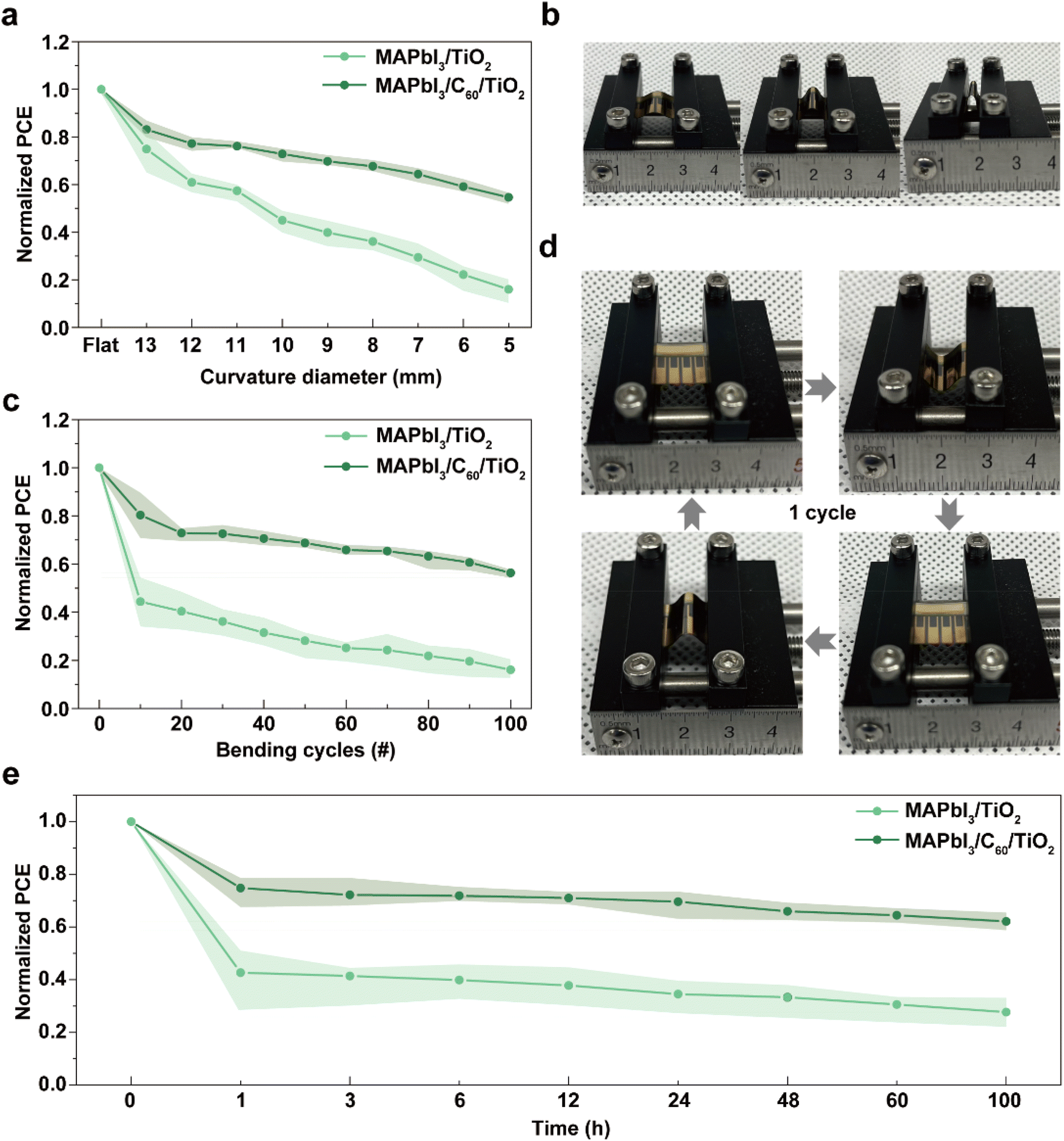 | ||
| Fig. 6 Stability test of SS-based flexible PSCs after bending: (a) PCE measured after bending the substrate to diameters ranging from flat to 5 mm. (b) Images of devices bent to diameters of 12 mm, 9 mm, and 5 mm. (c) PCE measured over bending cycles ranging from 0 to 100. (d) Images of the devices after 1 bending cycle. (e) PCE measured after bending the substrate within a specified bending time of 0 to 100 h. | ||
Conclusions
This work highlights the dual role of a 20 nm C60 interlayer in SS-based PSCs, demonstrating its contribution to both enhanced mechanical durability and photovoltaic performance under bending stress. The incorporation of C60 shifted the neutral axis closer to the brittle TiO2 layer and reduced the effective strain and stress by ∼20%, as supported by theoretical and experimental analysis. In addition, the C60 layer reduced Rp, mitigated the K, and improved charge extraction efficiency. Importantly, C60 provided structural protection to the electron transport layer while simultaneously enhancing the crystallinity of the active perovskite layer, resulting in greater resilience to mechanical deformation. As a result, C60-incorporated devices retained 6.2% higher PCE after bending compared to controls. These findings support the use of compliant interfacial layers such as C60 to simultaneously enhance the mechanical robustness and operational stability of PSCs, which is particularly relevant for emerging applications in BIPV and VIPV.Methods
Materials
SS 304 substrates with a thickness of 0.05T were used. Dimethyl sulfoxide (anhydrous, 99.9%) (DMSO), chlorobenzene (anhydrous, 99.9%), N,N-dimethylformamide (anhydrous, 99.8%) (DMF), acetonitrile (anhydrous, 99.8%), fullerene-C60, lead(II) iodide (PbI2), diethyl ether, 4-tert-butylpyridine (96%), and lithium bis(trifluoromethanesulfonyl)imide (Li-TFSI) were purchased from Sigma-Aldrich. Methylammonium iodide (MAI) was procured from dyesol, and 2,2′,7,7′-tetrakis [N,N-di(4-methoxyphenyl)amino]-9,9′-spirobifluorene (spiro-OMeTAD) was obtained from Lumtec.Fabrication of perovskite solar cell
The SS substrates were sequentially cleaned by sonication in acetone, ethanol, and isopropanol for 15 minutes each. Subsequently, the substrates were treated with ultraviolet (UV)-ozone for 30 minutes. To serve as a diffusion barrier, a 1 μm layer of SiO2 was deposited onto the SS substrates via plasma-enhanced chemical vapor deposition (PECVD). The TiO2 layer, with a target thickness of 50 nm, was fabricated through RF magnetron sputtering at a chamber pressure below 7 × 10⁻⁷ mTorr. C60 layers were deposited by thermal evaporation at varying thicknesses of 5, 10, 20, and 30 nm. A 1 M perovskite precursor solution was prepared by dissolving stoichiometric amounts of PbI2 and MAI in a 1:1 (v/v) mixture of DMSO and γ-butyrolactone (GBL). The solution was stirred at 70 °C for 2 hours and filtered using a 0.2 μm PTFE syringe filter. Subsequently, the solution was deposited onto the substrate using a two-step spin-coating process: 1000 rpm for 10 seconds, followed by 5000 rpm for 60 seconds. During the second step, 1000 μL of chlorobenzene was dropped onto the center of the perovskite film as an antisolvent to facilitate the crystallization of perovskite grains. The substrate was annealed at 100 °C for 1 hour to complete the crystallization of the perovskite layer. For the hole transport layer (HTL), spiro-OMeTAD powder was dissolved in a solution containing 28.8 μL of 4-tert-butylpyridine, 520 mg of Li-TFSI in 1 mL of acetonitrile, and 1 mL of chlorobenzene. The prepared solution was applied onto the substrate and spin-coated to form a thin layer. A 10 nm thick MoOx buffer layer was then thermally evaporated, followed by the deposition of a 160 nm thick ITO transparent electrode using RF magnetron sputtering. Finally, a 100 nm thick Au electrode was deposited through thermal evaporation.
Materials characterization
Scanning electron microscopy (SEM) was performed using a Quanta 250 FEG microscope (FEI). X-ray diffraction (XRD) patterns were obtained using an X-ray diffractometer (Rigaku) with Cu-Kα radiation (λ = 1.54 Å). X-ray photoelectron spectroscopy (XPS) measurements were conducted with a Thermo Scientific K-Alpha system equipped with a monochromated Al Kα X-ray source. Photoluminescence (PL) spectra were measured on a JASCO FP-8500 spectrofluorometer. Lifetime measurements were carried out using a 470 nm picosecond laser (PicoQuant, Germany) as the excitation source. Atomic force microscopy measurements were performed using a Dimension 3 Edge AFM system (Bruker). Conductive atomic force microscopy (C-AFM) was employed to measure conductivity using the Dimension Edge C-AFM system.Device characterization
A class AAA solar simulator was used to measure the J–V characteristics of the devices at a scanning rate of 0.05 V s−1, using a Keithley 2400 instrument. The AM 1.5G (1 sun, 100 mW cm−2) solar power was calibrated using a silicon reference solar cell. All J–V measurements were performed with a 0.075 cm2 mask, and the scan voltage setting time was 200 ms. The incident photon-to-current conversion efficiency (IPCE) was measured using equipment from HS Technology Inc. Electrochemical impedance spectroscopy measurements were conducted under simulated AM 1.5G illumination at an intensity of 1 mA cm−2 using an electrochemical measurement system (InviumStat.XR, Invium Technologies). EIS measurements were performed over a frequency range of 1 Hz to 1 MHz.Data availability
The data supporting this article have been included as part of the ESI.†Author contributions
H.-S. Lee and D. H. Kim supervised the overall project. H. J. Lee and K. Kim were responsible for developing concrete strategies, data curation, formal analysis, investigation, and writing the original draft and editing. S. Lee and D. Pyun performed data curation and formal analysis. J.-S. Hwang, J. Nam, S. Cho, and S.-H. Jeong performed formal analysis. D. Kim and Y. Kang performed project administration. All authors have read and approved the manuscript.Conflicts of interest
There are no conflicts to declare.Acknowledgements
This work was supported by the Korea Institute of Energy Technology Evaluation and Planning (KETEP) grant funded by the Korea government(MOTIE) (RS-2024-00451343). This work was supported by Basic Science Research Program (Priority Research Institute) through the NRF of Korea funded by the Ministry of Education (2021R1A6A1A10039823).References
- W. Yue, H. Yang, H. Cai, Y. Xiong, T. Zhou, Y. Liu, J. Zhao, F. Huang, Y.-B. Cheng and J. Zhong, Adv. Mater., 2023, 35, 2301548 CrossRef CAS PubMed
.
- A. Chatzipanagi, G. Kakoulaki, S. Szabó and A. Jäger-Waldau, Appl. Sci., 2024, 14, 10628 CrossRef CAS
- T. E. Kuhn, C. Erban, M. Heinrich, J. Eisenlohr, F. Ensslen and D. H. Neuhaus, Energy Build., 2021, 231, 110381 CrossRef
- B. Commault, T. Duigou, V. Maneval, J. Gaume, F. Chabuel and E. Voroshazi, Appl. Sci., 2021, 11, 11598 CrossRef CAS
- B. T. Feleki, R. K. M. Bouwer, V. Zardetto, M. M. Wienk and R. A. J. Janssen, ACS Appl. Energy Mater., 2022, 5, 6709 CrossRef CAS PubMed
- S. Lee, S.-W. Lee, S. Bae, J.-K. Hwang, W. Lee, D. Pyun, S.-H. Jeong, K. Kim, J.-S. Hwang, S. Cho, D. Kim, Y. Kang and H.-S. Lee, Energies, 2023, 16, 8061 CrossRef CAS
- J. Zheng, F.-J. Ma, C. Liao, J. Bing, S. Tang, A. M. Soufiani, R. L. Chin, C. Xue, J. Qu, L. Yang, M. A. Mahmud, Z. Sun, T. L. Leung, G. Wang, J. M. Cairney, S. Bremner, D. R. McKenzie, S. Huang and A. W. Y. Ho-Baillie, Cell Rep. Phys. Sci., 2023, 4, 101543 CrossRef CAS
- C. Zhou, Y. Xu, Y. Li, K. Du, X. Li, X. Dong, L. Li, N. Yuan and J. Ding, Sol. RRL, 2024, 8, 2300901 CrossRef CAS
- K. Ahn, S.-Y. Kim, S. Kim, D.-H. Son, S.-H. Kim, S. Y. Kim, J. H. Kim, S.-J. Sung, D.-H. Kim and J.-K. Kang, J. Mater. Chem. A, 2019, 7, 24891 RSC
- K. H. Jung, S. J. Yun, S. H. Lee, Y. J. Lee, K.-S. Lee, J. W. Lim, K.-B. Kim, M. Kim and R. E. I. Schropp, Sol. Energy Mater. Sol. Cells, 2016, 145, 368 CrossRef CAS
- L. Kranz, C. Gretener, J. Perrenoud, R. Schmitt, F. Pianezzi, F. L. La Mattina, P. Blösch, E. Cheah, A. Chirilă, C. M. Fella, H. Hagendorfer, T. Jäger, S. Nishiwaki, A. R. Uhl, S. Buecheler and A. N. Tiwari, Nat. Commun., 2013, 4, 2306 CrossRef PubMed
- K. Miettunen, J. Halme, M. Toivola and P. Lund, J. Phys. Chem. C, 2008, 112, 4011 CrossRef CAS
- J. Liu, Z. Zhao, J. Qian, Z. Liang, C. Wu, K. Wang, S. Liu and D. Yang, Adv. Mater., 2024, 36, 2401236 CrossRef CAS PubMed
- J. Liu, T. Ye, D. Yu, S. Liu and D. Yang, Angew. Chem., Int. Ed., 2023, 62, e202307225 CrossRef CAS PubMed
- Y. Ma, Z. Lu, X. Su, G. Zou and Q. Zhao, Adv. Energy Syst. Res., 2023, 4, 2200133 CAS
- J. Zhang, W. Zhang, H.-M. Cheng and S. R. P. Silva, Mater. Today, 2020, 39, 66 CrossRef CAS
- Z. Li, C. Jia, J. Cao, J. Shi, J. Xue, X. Liu, H. Wu, C. Xiao, C. Li, M. Li, C. Zhang and Z. Li, Nat. Commun., 2025, 16, 1771 CrossRef CAS PubMed
- D. A. Chalkias, A. Nikolakopoulou, L. C. Kontaxis, A. N. Kalarakis and E. Stathatos, Adv. Funct. Mater., 2024, 34, 2406354 CrossRef CAS
- L. Dong, S. Qiu, J. G. Cerrillo, M. Wagner, O. Kasian, S. Feroze, D. Jang, C. Li, V. M. L. Corre, K. Zhang, H. Peisert, F. U. Kosasih, C. Ducati, C. Arrive, T. Du, F. Yang, C. J. Brabecm and H.-J. Egelhaaf, Energy Environ. Sci., 2024, 17, 7091–7106 Search PubMed
- W. Xu, B. Chen, Z. Zhang, Y. Liu, Y. Xian, X. Wang, Z. Shi, H. Gu, C. Fei, N. Li, M. A. Uddin, H. Zhang, L. Dou, Y. Yan and J. Huang, Nat. Protoc., 2024, 18, 379 CAS
- H. Liang, W. Yang, J. Xia, H. Gu, X. Meng, G. Yang, Y. Fu, B. Wang, H. Cai, Y. Chen, S. Yang and C. Liang, Adv. Sci., 2023, 10, 2304733 CrossRef CAS PubMed
- X. Hu, Z. Huang, X. Zhou, P. Li, Y. Wang, Z. Huang, M. Su, W. Ren, F. Li, M. Li, Y. Chen and Y. Song, Adv. Mater., 2017, 29, 1703236 CrossRef PubMed
- G. Lee, M.-C. Kim, Y. W. Choi, N. Ahn, J. Jang, J. Yoon, S. M. Kim, J.-G. Lee, D. Kang, H. S. Jung and M. Choi, Energy Environ. Sci., 2019, 12, 3182 RSC
- H. P. Parkhomenko, Y. Yerlanuly, V. V. Brus and A. N. Jumabekov, Org. Electron., 2024, 129, 107049 CrossRef CAS
- N. Rolston, K. A. Bush, A. D. Printz, A. Gold-Parker, Y. Ding, M. F. Toney, M. D. McGehee and R. H. Dauskardt, Adv. Energy Mater., 2018, 8, 1802139 CrossRef
- Q. Dong, M. Chen, Y. Liu, F. T. Eickemeyer, W. Zhao, Z. Dai, Y. Yin, C. Jiang, J. Feng, S. Jin, S. Liu, S. M. Zakeeruddin, M. Grätzel, N. P. Padture and Y. Shi, Joule, 2021, 5, 1587 CrossRef CAS
- Y. Guo, J. Cheng, L. Liu and Z. Tan, Mater. Lett., 2021, 292, 129559 CrossRef CAS
- A. A. Alsayed, J. Appl. Math. Phys., 2021, 9, 176 CrossRef
- C. Wang, L. Ma, D. Guo, X. Zhao, Z. Zhou, D. Lin, F. Zhang, W. Zhao, J. Zhang and Z. Nie, J. Mater. Chem. C, 2020, 8, 3374 RSC
- S. F. Wen, W. Z. Yan, J. X. Kang, J. Liu and Z. F. Yue, Appl. Surf. Sci., 2010, 257, 1289 CrossRef CAS
- R. Saleh, M. Barth, W. Eberhardt and A. Zimmermann, Micromachines, 2021, 12, 78 CrossRef PubMed
- B. Li, X. Wu, H. Zhang, S. Zhang, Z. Li, D. Gao, C. Zhang, M. Chen, S. Xiao, A. K.-Y. Jen, S. Yang and Z. Zhu, Adv. Funct. Mater., 2022, 32, 2205870 CrossRef CAS
- X. Yu, W. Ge, L. Fan, B. Fan, R. Peng and B. Jin, J. Colloid Interface Sci., 2023, 650, 553 CrossRef CAS PubMed
- K.-W. Tsai, C.-C. Chueh, S. T. Williams, T.-C. Wen and A. K. Y. Jen, J. Mater. Chem. A, 2015, 3, 9128 RSC
- L.-C. Chen, Y.-S. Lin, Z.-L. Tseng, C. Wu, F.-S. Kao and S.-H. Chen, Nanomaterials, 2017, 7, 166 CrossRef PubMed
- N. Klipfel, A. O. Alvarez, H. Kanda, A. A. Sutanto, C. Igci, C. Roldán-Carmona, C. Momblona, F. Fabregat-Santiago and M. K. Nazeeruddin, ACS Appl. Energy Mater., 2022, 5, 1646 CrossRef CAS
- H.-S. Lin, I. Jeon, R. Xiang, S. Seo, J.-W. Lee, C. Li, A. Pal, S. Manzhos, M. S. Goorsky, Y. Yang, S. Maruyama and Y. Matsuo, ACS Appl. Mater. Interfaces, 2018, 10, 39590 CrossRef CAS PubMed
- Y.-Q. Zhou, B.-S. Wu, G.-H. Lin, Z. Xing, S.-H. Li, L.-L. Deng, D.-C. Chen, D.-Q. Yun and S.-Y. Xie, Adv. Energy Mater., 2018, 8, 1800399 CrossRef
- F. Ye, S. Zhang, J. Warby, J. Wu, E. Gutierrez-Partida, F. Lang, S. Shah, E. Saglamkaya, B. Sun, F. Zu, S. Shoaee, H. Wang, B. Stiller, D. Neher, W.-H. Zhu, M. Stolterfoht and Y. Wu, Nat. Commun., 2022, 13, 7454 CrossRef CAS PubMed
- V. Arivazhagan, J. Xie, P. Hang, M. M. Manonmani Parvathi, A. Khan, C. Cui, D. Yang and X. Yu, J. Phys. D, 2019, 52, 225104 CrossRef CAS
- J. Y. Kim, J.-W. Lee, H. S. Jung, H. Shin and N.-G. Park, Chem. Rev., 2020, 120, 7867 CrossRef CAS PubMed
- D. Liu, Q. Wang, C. J. Traverse, C. Yang, M. Young, P. S. Kuttipillai, S. Y. Lunt, T. W. Hamann and R. R. Lunt, ACS Nano, 2018, 12, 876 CrossRef CAS PubMed
- P.-W. Liang, C.-C. Chueh, S. T. Williams and A. K.-Y. Jen, Adv. Energy Mater., 2015, 5, 1402321 CrossRef
- K. Wojciechowski, S. D. Stranks, A. Abate, G. Sadoughi, A. Sadhanala, N. Kopidakis, G. Rumbles, C.-Z. Li, R. H. Friend, A. K.-Y. Jen and H. J. Snaith, ACS Nano, 2014, 8, 12701 CrossRef CAS PubMed
- S. Moore, R. Burrows, D. Kumar, M. B. Kloucek, A. D. Warren, P. E. J. Flewitt, L. Picco, O. D. Payton and T. L. Martin, npj Mater. Degrad., 2021, 5, 3 CrossRef CAS
- Y. Zhao, W. Zhou, W. Ma, S. Meng, H. Li, J. Wei, R. Fu, K. Liu, D. Yu and Q. Zhao, ACS Energy Lett., 2016, 1, 266 CrossRef CAS
- Y. Li, Y. Zhao, Q. Chen, Y. M. Yang, Y. Liu, Z. Hong, Z. Liu, Y.-T. Hsieh, L. Meng, Y. Li and Y. Yang, J. Am. Chem. Soc., 2015, 137, 15540 CrossRef CAS PubMed
- D. Arola and C. L. Williams, Int. J. Fatig., 2002, 24, 923 CrossRef CAS
-
W. D. Pilkey, D. F. Pilkey and Z. Bi, Peterson's Stress Concentration Factors, Wiley, Hoboken, NJ, 4th edn, 2020 Search PubMed
- H. Si, S. Zhang, S. Ma, Z. Xiong, A. Kausar, Q. Liao, Z. Zhang, A. Sattar, Z. Kang and Y. Zhang, Adv. Energy Mater., 2020, 10, 1903922 CrossRef CAS
- M. Kim, J. Kwon, H. J. Lee, K. S. Park, J. Kim, J. Kim, K. Baek, H. Yuan, J. K. Hyun, Y. S. Cho, J. Yeom and D. H. Kim, Nano Energy, 2023, 114, 108680 CrossRef CAS
- C. Guo, J. Chen, G. Li, X. Liang, W. Lai, L. Yang, Y. Mai and Z. Li, Glob. Chall., 2019, 3, 1800108 CrossRef PubMed
- A. A. Said, E. Aydin, E. Ugur, Z. Xu, C. Deger, B. Vishal, A. Vlk, P. Dally, B. K. Yildirim, R. Azmi, J. Liu, E. A. Jackson, H. M. Johnson, M. Gui, H. Richter, A. R. Pininti, H. Bristow, M. Babics, A. Razzaq, S. Mandal, T. G. Allen, T. D. Anthopoulos, M. Ledinský, I. Yavuz, B. P. Rand and S. De Wolf, Nat. Commun., 2024, 15, 708 CrossRef CAS PubMed
- L. Chen, C. Xu, Y. Qin, X. He, H. Bian, G. Xu, L. Niu and Q. Song, Nanomaterials, 2022, 12, 1736 CrossRef CAS PubMed
Footnotes |
| † Electronic supplementary information (ESI) available. See DOI: https://doi.org/10.1039/d5el00037h |
| ‡ These authors contributed equally to the work. |
| This journal is © The Royal Society of Chemistry 2025 |