
Bimolecular amine vapor passivation for efficient perovskite solar cells based on blade-coated FAPbI3
Cun
Zhou†
a,
Weicheng
Wang†
a,
Haotian
Wu†
ab,
Jinsen
Zhang
 c,
Ying
Zhou
a,
Yao
Wang
*c,
Gang
Wu
a,
Weifei
Fu
*b,
Alex K.-Y.
Jen
d and
Hongzheng
Chen
*ab
c,
Ying
Zhou
a,
Yao
Wang
*c,
Gang
Wu
a,
Weifei
Fu
*b,
Alex K.-Y.
Jen
d and
Hongzheng
Chen
*ab
aState Key Laboratory of Silicon and Advanced Semiconductor Materials, International Research Center for X Polymers, Department of Polymer Science and Engineering, Zhejiang University, Hangzhou, 310058, China. E-mail: hzchen@zju.edu.cn
bZhejiang University-Hangzhou Global Scientific and Technological Innovation Center, Hangzhou, 311200, China. E-mail: zjufwf@zju.edu.cn
cCollege of Materials Science and Engineering, Zhejiang University of Technology, Hangzhou, 310014, China. E-mail: wangyao@zjut.edu.cn
dDepartment of Chemistry, Department of Material Science & Engineering, City University of Hong Kong, Kowloon, Hong Kong 999077, China
First published on 6th September 2025
Abstract
Formamidinium lead triiodide (FAPbI3)-based perovskite solar cells (PSCs) are highly promising due to their optimal bandgaps and high efficiencies, but suffer from instability and performance-limiting defects. Conventional solution-based passivation methods face challenges in surface uniformity and scalability. Here, a bimolecular amine vapor passivation (BAVP) strategy using 2-phenylethylamine (PEA) and ethylenediamine (EDA) is introduced to effectively passivate blade-coated FAPbI3 films fabricated under ambient low-humidity conditions, with excellent surface uniformity. PEA coordinates with Pb2+ to mitigate surface defects, while EDA reacts preferentially with FA+, optimizing energy alignment at the perovskite/C60 interface for enhanced charge extraction. Consequently, BAVP-treated PSCs achieve a champion efficiency of 25.2%. Remarkably, unencapsulated devices retain 99.4% of their initial efficiency after 2616 hours of thermal aging at 85 °C in N2 (ISOS-D-2), and 97.5% after 500 thermal cycles (ISOS-T-1) in N2. Furthermore, perovskite solar modules (PSMs) fabricated using the BAVP method attain an efficiency of 21.3% over a total area of 6.25 cm2, surpassing the 18.7% obtained using the traditional solution-based passivation. These results demonstrate the significant potential of the BAVP strategy in advancing the efficiency, stability and scalability of PSCs.
Broader contextPerovskite solar cells (PSCs) are promising candidates for next-generation photovoltaics due to their low-cost fabrication, high efficiency, and scalability. However, their commercialization remains limited by performance-reducing defects and insufficient stability. Conventional solution-based passivation methods often encounter issues of poor film uniformity, especially for large-area device fabrication. Here, we introduce a vapor-based bimolecular amine passivation strategy, significantly improving the film uniformity and effectively reducing defects in blade-coated perovskite layers. This approach enables higher device efficiency and outstanding thermal stability, especially beneficial for large-area perovskite solar modules, thereby addressing critical obstacles toward commercializing perovskite photovoltaics. Our approach thus represents a meaningful advance toward large-scale manufacturing of highly efficient and stable PSCs, contributing positively to global renewable energy development and carbon neutrality targets. |
Introduction
Perovskite solar cells (PSCs) have attracted significant attention from both academia and industry as one of the most promising thin-film photovoltaic technologies due to their easy solution processibility, large-area printability, low cost and high power conversion efficiencies (PCEs), which are comparable to those of silicon solar cells.1–10 Among all reported perovskite materials, formamidinium lead triiodide (FAPbI3) is one of the most promising candidates for single junction PSCs with high PCEs owing to its suitable optical band gap of 1.50 eV.11,12 Unfortunately, the FAPbI3 perovskite suffers from undesirable phase instability, which can be accelerated by the defects at interfaces and grain boundaries.13,14 These defects also limit the device performance. Thus, many pioneer works have been conducted to passivate the defects of perovskites with Lewis acid/base groups,15–17 ammonium halide salts18,19 and cationic metal ions20,21 for higher PCEs and better long-term stability of FAPbI3 PSCs. Most passivation is carried out using solution-based methods, such as spin-coating, which inevitably face compatibility challenges in large-area device fabrication.22–25 In contrast, vapor-assisted passivation can avoid the disadvantages of surface inhomogeneity and reconstruction caused by solvents, although this strategy has been less explored, especially in the fabrication of large-area devices and modules.22,26–28 On the other hand, combining different passivation molecules with distinct functionalities has been shown to effectively address the complex interface carrier recombination issues in PSCs, but this was also less investigated,29,30 and the unique functionalities of these passivation molecules still require further exploration to achieve an optimized combination. Additionally, most FAPbI3 PSCs are fabricated via the spin-coating technique in a nitrogen atmosphere, which is incompatible with high-throughput manufacture of large-area perovskite solar modules (PSMs). In contrast, blade-coating, a simple deposition method with a high ink utilization rate, is considered one of the most promising candidates for scalable PSM fabrication.31–34In this study, a bimolecular amine vapor passivation (BAVP) strategy was used to achieve uniform and efficient passivation aiming for high efficiency blade-coated FAPbI3 PSCs and PSMs. 2-Phenylethylamine (PEA) and ethylenediamine (EDA) with different coordination ability and surface reactivity towards FAPbI3 were combined to passivate surface defects on the surface of FAPbI3 perovskite films and optimize energy level alignment at the perovskite/C60 interface, thereby suppressing carrier recombination and enhancing charge extraction. As a result, a champion PCE of 25.2% was achieved for inverted blade-coated FAPbI3 PSCs with BAVP treatment, fabricated under low-humidity air conditions. Moreover, unencapsulated PSCs exhibited remarkable thermal stability, retaining 99.4% of their initial efficiency after 2616 hours at 85 °C, and excellent thermal cycling stability, maintaining 97.5% of their efficiency after 500 thermal cycles between −5 and 55 °C in a glovebox. Furthermore, minimodules were also fabricated and a PCE of 21.3% was achieved with a total module area of 6.25 cm2, clearly surpassing modules fabricated via traditional solution-based passivation (18.7%).
Results and discussion
The FAPbI3 perovskite films were prepared using a dry-air-knife assisted blade-coating technique in low-humidity air (Fig. 1a). The BAVP was carried out after annealing the perovskite films at 120 °C for 30 min. In the BAVP process, a Petri dish containing diluted PEA and EDA in toluene was heated until the amines were fully vaporized. The annealed FAPbI3 films were then placed into the Petri dish and heated at an optimized temperature of 70 °C to facilitate interaction with the vaporized amines. This strategy aimed to optimize the perovskite surface by combing two passivators with distinct functionalities, PEA and EDA. Owing to its strong coordination ability, PEA could form coordination bonds with Pb2+ on the FAPbI3 perovskite surface to reduce deep traps.35,36 For EDA, with its higher nucleophilicity, it may prefer to react with surface FA+ ions, promoting the formation of iodine vacancies (VI), which are usually positively charged shallow traps, enhancing the built-in electric field and thus optimizing charge extraction.37,38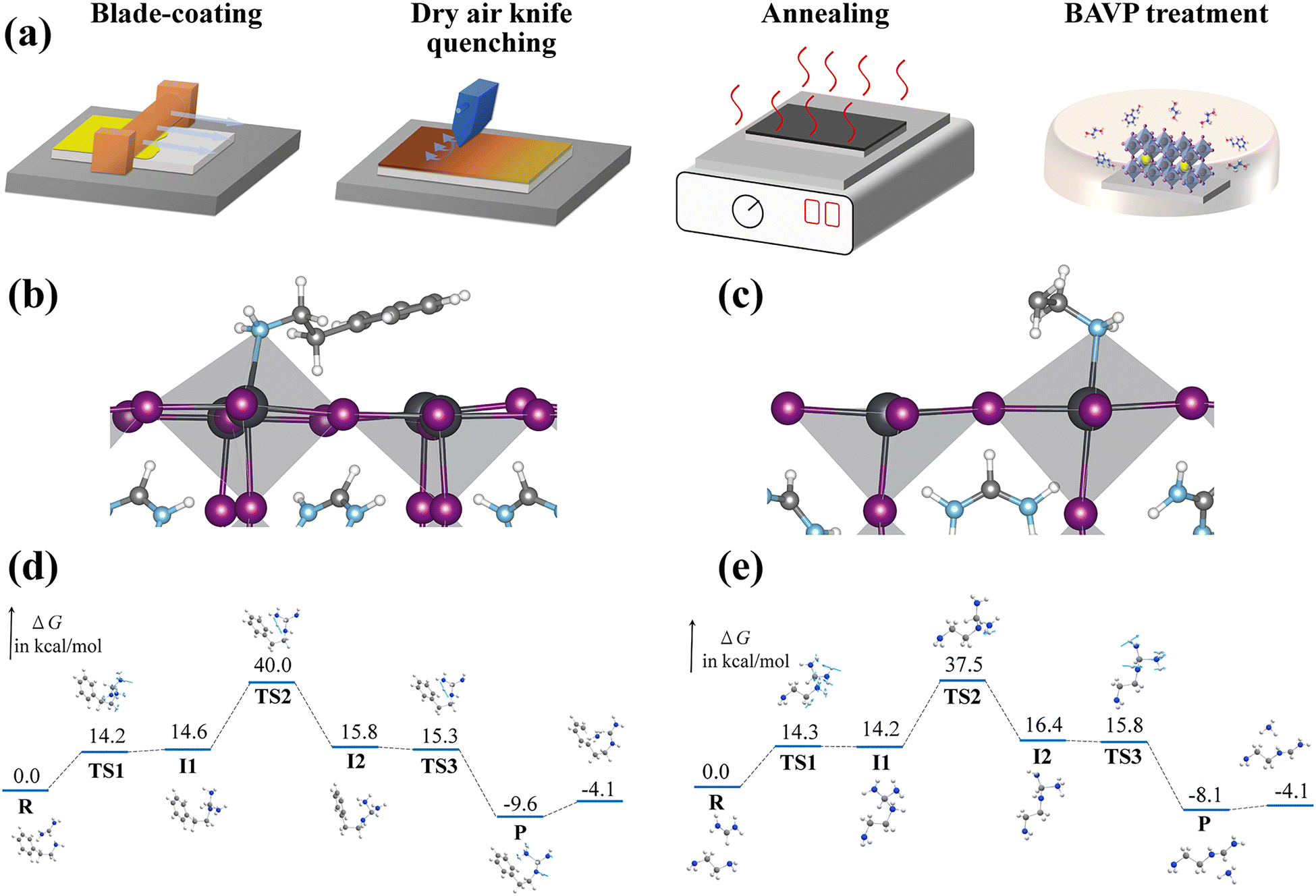 | ||
| Fig. 1 (a) Schematics of the BAVP process for blade-coated FAPbI3 perovskite films. Schematic diagrams showing the adsorption of (b) PEA and (c) EDA on PbI2-terminated FAPbI3 surfaces. Gibbs free energy profiles of the reaction of (d) PEA and (e) EDA with FA+. | ||
Density functional theory (DFT) calculations were performed to provide insights into the different interactions of PEA and EDA with the FAPbI3 perovskite. We firstly compared the binding energies of amines with the PbI2-terminated FAPbI3 surface. The DFT results showed that PEA chemically bonds to the PbI2-terminated surface with a binding energy of 3.40 eV (Fig. 1b), while the binding energy calculated for EDA with perovskite was 3.27 eV (Fig. 1c), indicating that PEA is more likely to bind to the PbI2-terminated FAPbI3 surface. Gibbs free energy profiles of the reaction between PEA or EDA and FA+ were also calculated (Fig. 1d and e and Scheme S1). The theoretical studies revealed that, after forming a complex between the amines and FA+, a nucleophilic attack by the amino group in either PEA or EDA on FA+ proceeds through a transition state (TS1), forming an intermediate (I1). A subsequent proton shift process via the transition state (TS2) yields a second intermediate (I2). The activation free energy for the reaction between EDA and FA+ (37.5 kcal mol−1) was found to be lower than that of the reaction involving PEA and FA+ (40 kcal mol−1). This indicates that EDA is more reactive towards FA+. These theoretical calculations demonstrate that PEA preferentially interacts with the PbI2-terminated surface, while EDA is more likely to react with FA+, highlighting their complementary roles in surface passivation.
X-ray photoelectron spectroscopy (XPS) was performed to experimentally validate the interactions between the amines and the perovskite. The peaks observed at 138.4 and 143.25 eV are assigned to Pb 4f7/2 and Pb 4f5/2, respectively (Fig. 2a).39 The corresponding peaks shifted towards lower binding energy significantly with PEA vapor passivation, confirming the successful passivation of uncoordinated Pb2+ on the surface. In contrast, the EDA vapor-treated film exhibited negligible shift in the lead peaks. X-ray diffraction (XRD) results also show that the peak area of PbI2 in the PEA-treated film decreased, indicating the effective coordination of PEA with PbI2 to passivate surface defects (Fig. S1). This is consistent with the XPS results.40 These experimental findings align well with our theoretical calculations described previously, providing complementary evidence of distinct amine-perovskite interactions.
 | ||
| Fig. 2 (a) XPS spectra of Pb 4f for the control, PEA vapor, EDA vapor and BAVP-treated perovskite films. KPFM images of (b) solution-passivated and (c) BAVP-treated FAPbI3 perovskite films. Depth-resolved GIXRD spectra of (d) the control, (e) BAVP and (f) solution-passivated FAPbI3 perovskite films at different Ψ angles (from 5° to 45°). | ||
The solution passivated perovskite films may suffer surface inhomogeneity and reconstruction caused by solvents, especially for large area perovskite films. Therefore, the surface morphology and homogeneity after solution and vapor passivation with PEA/EDA mixed amines were investigated by scanning electron microscopy (SEM) (Fig. S2), atomic force microscopy (AFM) (Fig. S3) and Kelvin probe force microscopy (KPFM) (Fig. 2b and c). SEM and AFM images revealed no obvious morphological changes after various types of passivation (Fig. S2 and S3). However, the surface potential of the BAVP-treated film with a narrow potential distribution of 5.5 mV was notably more uniform than that of the solution-treated film with a wider potential distribution of 12.2 mV, which is crucial for achieving homogeneous optoelectronic properties across the film (Fig. 2b and c). Furthermore, grazing incidence X-ray diffraction (GIXRD) analysis showed a substantial release of residual tensile strain in the BAVP-treated film compared to the solution passivated film, highlighting the superior effectiveness and uniformity of the BAVP strategy (Fig. 2d–f and Fig. S4).38
Ultraviolet photoelectron spectroscopy (UPS) was carried out to analyze the band edge positions of perovskite films without and with different amine vapor treatments (Fig. S5). PEA vapor treatment only slightly changes the energy levels of the perovskite, while EDA vapor treatment led to a significant shift in both the valence band maximum (EVBM) and the Fermi level (EF). The downward shift of energy levels at the perovskite surface is attributed to the formation of the new species N-(2-aminoethyl)-formamidinium (AEFA), produced via the reaction between EDA and FA+. The dipole moment of AEFA was calculated to be 5.57 D (Fig. S6). The passivation did not change the bandgaps, as demonstrated by the UV-vis absorption spectra (Fig. S7) and corresponding Tauc plots (Fig. S8). Therefore, the conduction band minimum (ECBM) was obtained by adding the optical bandgap to EVBM, and the resulting energy level diagrams of the PSCs with different amine treatments are presented in Fig. 3a. The BAVP-treated films incorporating both PEA and EDA also show significantly downshifted EVBM and ECBM, resulting in improved energy level alignment between the perovskite and C60, which facilitates more efficient electron extraction.41 To further evaluate electron extraction and hole blocking capabilities, the energy level differences between the ECBM and the Fermi level (EF) of the perovskite films were calculated (Fig. 3b). Treatments with PEA, EDA and BAVP effectively reduced the energy offset from 0.68 eV in the untreated film to 0.64 eV, 0.24 eV and 0.37 eV, respectively, thereby creating favorable n-type surface energetics and enhanced band bending for improved charge extraction and hole blocking.29
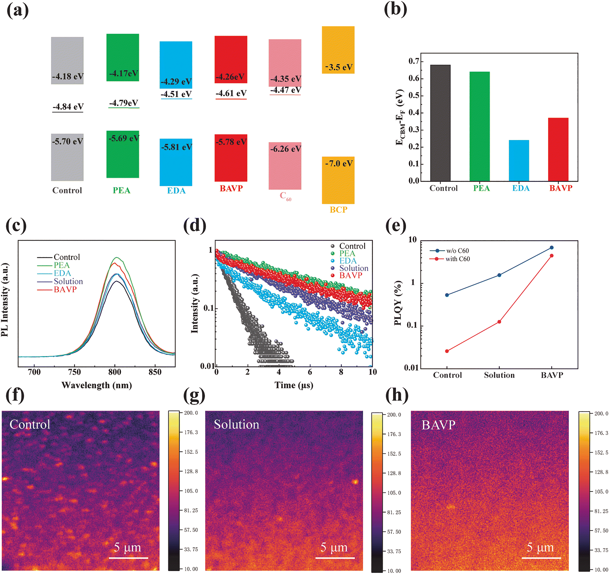 | ||
| Fig. 3 (a) Energy level alignment and (b) energy offset between ECBM and EF of perovskite films without and with different amine vapor treatments. (c) Steady-state PL spectra, (d) TRPL decay curves, (e) PLQY values and (f)–(h) PL mapping of perovskite films without and with different passivation methods using different amines. | ||
We further performed steady-state photoluminescence (PL) and time-resolved photoluminescence (TRPL) to investigate the carrier recombination and transfer behaviors in FAPbI3 films treated with different amines using different methods. The PL intensity increased notably after both PEA and EDA vapor treatments, indicating the suppressed non-radiative recombination with reduced defects (Fig. 3c).42 The TRPL results also showed that the average carrier lifetimes (τ) of FAPbI3 films increased significantly from 0.76 μs (control) to 6.63 μs, 2.82 μs and 6.44 μs for films passivated with PEA, EDA, and BAVP treatments, respectively (Fig. 3d). Among them, PEA showed the highest individual effectiveness in prolonging carrier lifetimes due to its strong capability to passivate surface-related defects and effectively suppress non-radiative recombination. EDA vapor treatment also extended the lifetime to 2.82 μs, confirming its significant role in reducing surface defects.
We further compared the traditional solution-based passivation and our BAVP strategy. The solution-treated films achieved a carrier lifetime of 4.02 μs, which is much shorter than the 6.44 μs achieved with BAVP-treated films. This highlights that the BAVP approach offers more comprehensive defect passivation than traditional solution-based passivation. Moreover, PL quantum yield (PLQY) data presented in Fig. 3e further corroborate these observations. The unpassivated film exhibits very low PLQY (∼0.5%), while solution-treated films improve PLQY to ∼1.5%, and BAVP-treated films reach ∼7% for bare films and ∼4.5% for perovskite/C60 stacks. This pronounced increase of PLQY, especially at the perovskite/C60 interface, underscores significantly reduced non-radiative recombination pathways and enhanced interfacial quality with BAVP passivation. Fig. 3(f–h) shows PL intensity mappings of FAPbI3 films subjected to different passivation methods. The control film exhibits pronounced PL intensity fluctuations, featuring notable bright and dark spots indicative of significant localized non-radiative recombination. Although the solution-treated film shows improvement, evident heterogeneity remains. In contrast, the BAVP-treated film displays a substantially more uniform PL intensity distribution, characterized by consistent brightness and reduced hotspots. Uniform PL intensity mapping is recognized as a reliable indicator of film quality and reproducibility in perovskite photovoltaics, with more homogeneous films consistently yielding narrower performance distributions and improved device efficiencies.43 These observations strongly suggest that BAVP significantly enhances film-level optoelectronic homogeneity, potentially leading to improved device performance and reproducibility in both small-area cells and mini-modules.
Inverted PSCs with a device structure of ITO/NiOx/Me-4PACz/perovskite/C60/BCP/Ag were fabricated to investigate how amines used in vapor-based passivation methods, as well as the passivation methods themselves (solution-based vs. vapor-based), affect device performance (Fig. 4a). The effects of different amines in vapor-based passivation on device performance were firstly carefully investigated. The corresponding J–V curves of the devices are shown in Fig. 4b, and the detailed photovoltaic parameters are summarized in Table 1. With a device area of 0.058 cm2, the control device shows a PCE of 23.1% with an open-circuit voltage (VOC) of 1.10 V, a short circuit current density (JSC) of 26.0 mA cm−2, and a fill factor (FF) of 81.0% under reverse scan. Both PEA and EDA could improve the device performance individually to 24.4% and 25.0%, respectively, due to the effective defect passivation ability of PEA and the effective energy level alignment tunability of EDA. The BAVP-treated devices show the highest PCE of 25.2% with a VOC of 1.14 V, a JSC of 26.3 mA cm−2, and an FF of 84.4% under reverse scan attributed to the advantages of combing functionalities of PEA and EDA. This is also higher than the PCE of the solution-treated PSC which exhibited a PCE of 24.8% with a VOC of 1.13 V, a JSC of 26.3 mA cm−2, and an FF of 83.4% under reverse scan (Fig. 4c). The BAVP-treated device also shows a significantly reduced hysteresis (Table S1). To the best of our knowledge, it represents one of the highest reported PCEs for the blade-coated inverted FAPbI3 PSCs (Fig. 4d and Table S2). The vapor-treated devices also exhibited excellent reproducibility with a narrow efficiency distribution (Fig. S9). EQE and the corresponding integrated photocurrent curves are shown in Fig. 4e. The integration of photocurrents for devices matches well with the JSC values from the J–V curves.
 | ||
| Fig. 4 (a) Device structure of the inverted PSCs used in this work. The J–V curves of the best small area devices (b) without and with different amine vapor treatments and (c) with solution-based or vapor-based passivation methods using PEA/EDA mixed amines. (d) Representative PCEs of inverted FAPbI3-based PSCs and PSMs fabricated by blade-coating methods. (e) EQE spectra of the small area devices without and with different passivation methods using different amines. (f) The J–V curves and images of PSMs with different passivation methods. (g) The electrochemical impedance spectroscopy and (h) transient photocurrent of the devices without and with different amine vapor treatments. (i) SCLC characteristics of the electron-only devices without and with different amine vapor treatments. | ||
| Amine | V OC [V] | J SC [mA cm−2] | FF [%] | PCE [%] | J cal. [mA cm−2] |
|---|---|---|---|---|---|
| a Mini-modules with a total area of 6.25 cm2. | |||||
| w/o | 1.10 | 26.0 | 81.0 | 23.1 | 25.6 |
| (1.09 ± 0.01) | (26.0 ± 0.1) | (80.6± 0.5) | (22.9 ± 0.1) | ||
| PEA | 1.13 | 26.1 | 83.1 | 24.4 | 25.4 |
| (1.13± 0.01) | (26.2 ± 0.2) | (82.0 ± 0.6) | (24.2 ± 0.1) | ||
| EDA | 1.13 | 26.1 | 84.4 | 25.0 | 25.5 |
| (1.12 ± 0.01) | (26.2 ± 0.2) | (84.3 ± 0.7) | (24.8 ± 0.1) | ||
| BAVP | 1.14 | 26.3 | 84.3 | 25.2 | 25.8 |
| (1.13 ± 0.01) | (26.2 ± 0.1) | (83.8 ± 0.2) | (25.0 ± 0.1) | ||
| PEA&EDA/toluene | 1.13 | 26.3 | 83.4 | 24.8 | 25.6 |
| (1.13 ± 0.01) | (26.1 ± 0.2) | (83.0 ± 0.8) | (24.5 ± 0.2) | ||
| BAVPa | 5.77 | 4.74 | 77.7 | 21.3 | |
| PEA&EDA/toluenea | 5.68 | 4.56 | 72.2 | 18.7 | |
Perovskite solar modules (PSMs) were further fabricated to verify the advantages of vapor passivation for upscaling. The modules consist of 5 sub-cells connected in series by P1–P2–P3 laser line patterning with a geometric fill factor (GFF) of 94.8%. The total area of the module is 6.25 cm2 and the efficient active layer area is 5.925 cm2. The perovskite layers were fabricated via blade-coating and were passivated with solution and vapor passivation methods using PEA and EDA mixed amines. The PCE of the solution passivated PSM is 18.7% with a VOC of 5.68 V, a JSC of 4.56 mA cm−2 and an FF of 72.2%, while the vapor passivated PSM shows a much higher PCE of 21.3% with a VOC of 5.77 V, a Jsc of 4.74 mA cm−2 and an FF of 77.7% (Fig. 4f). When calculated with respect to the active area, the PCE reaches up to 22.5%. To the best of our knowledge, it also represented one of the highest reported PCEs for the blade-coated inverted FAPbI3 PSMs (Fig. 4d and Table S2), demonstrating the superiority of vapor passivation for upscaling.
To further explore the distinct roles of PEA and EDA in optimizing device performance, the carrier recombination was investigated by electrochemical impedance spectroscopy (EIS) at external bias under the dark condition to satisfy the depletion approximation for the measurement (Fig. 4g). According to the Nyquist plots, the fitted charge recombination resistance (Rrec) values were 855 Ω, 1262 Ω, 1566 Ω, and 1884 Ω for the control, PEA vapor, EDA vapor, and BAVP-treated devices, respectively. The increased Rrec of the amine vapor-treated devices indicated the reduced trap-assisted charge recombination in the devices.44 Notably, the BAVP-treated devices exhibited the highest Rrec, attributed to the superior defect passivation ability of PEA and the optimized energy level alignment by EDA.45,46 Transient photocurrent (TPC) measurements were further conducted to distinguish the role of EDA and PEA in BAVP-treated devices (Fig. 4h). The EDA-passivated device exhibits a shorter TPC decay time of 1.02 μs compared to the PEA-passivated device (1.42 μs), indicative of faster carrier extraction and transfer which could be attributed to the improved energy level alignment.25 Additionally, space charge limited current (SCLC) measurements were performed through electron-only devices with the configuration of ITO/SnO2/perovskite/C60/Ag to assess electron trap state densities (Ntrap) in different devices (Fig. 4i). The lowest trap-filled limited voltage (VTFL) of 0.124 V corresponds to an Ntrap of 4.45 × 1014 cm−3. This value is lower than those of the control (7.08 × 1014 cm−3), EDA-treated (5.48 × 1014 cm−3) and BAVP-treated (5.35 × 1014 cm−3) devices, highlighting the superior defect passivation achieved by PEA.47 These results confirm that PEA effectively reduces defects, while EDA facilitates enhanced charge extraction by optimizing the energy level alignment.
We further compared the effectiveness of traditional solution-based passivation and the vapor-based BAVP method using the same characterization techniques described above. EIS results showed that the recombination resistance (Rrec) for solution-treated films was approximately 1393 Ω (Fig. 3g), significantly lower than the 1884 Ω achieved with BAVP-treated films, indicating that BAVP provides more comprehensive suppression of trap-mediated recombination. TPC analysis further supported this finding, showing that BAVP-treated films exhibited much faster carrier extraction dynamics with a decay time of 1.05 μs than that of solution-treated films with a decay time of 1.80 μs, reflecting optimized interfacial properties. In addition, SCLC measurements demonstrated that BAVP treatment resulted in a lower Ntrap (5.35 × 1014 cm−3) compared to solution treatment (5.53 × 1014 cm−3), further confirming the superior electron trap passivation capability of the vapor-based approach. Collectively, these results highlight that the BAVP method outperforms traditional solution-based passivation in simultaneously reducing defects and enhancing carrier extraction, thus providing superior overall device performance.
Stability assessments were also performed to demonstrate the benefits of the BAVP strategy in enhancing the device stability. To evaluate the thermal stability of the PSCs, the unencapsulated PSCs were stored at 85 °C on a hot plate in a nitrogen-filled glovebox according to the ISOS-D-2 protocol. The BAVP treated PSC exhibited excellent thermal stability, maintaining 99.4% of the initial PCE after 2616 hours. In contrast, the control device showed rapid degradation within 100 hours (Fig. 5a). Additionally, to investigate the impact of day–night temperature differences on BAVP-based devices, the relationship of PCE and thermal cycles was measured at a temperature range of −5 to 55 °C (hold at each temperature for 5 min) according to the ISOS-T-1 protocol. The unencapsulated BAVP treated PSC retained 97.5% of its initial PCE after 500 times of thermal cycling, while the control device kept only 82.5% of its initial PCE (Fig. 5b). An initial evaluation of operational stability was also conducted under constant 1-sun illumination at 65 °C in air with ∼50% relative humidity according to the ISOS-L-3 protocol. The encapsulated BAVP-treated device exhibited remarkable robustness, retaining 97.9% of its initial PCE after 51 hours, whereas the control device maintained 91.7% of its initial PCE under the same conditions (Fig. S10). These results demonstrate the advantages of the BAVP strategy to achieve highly efficient and stable PSCs (Table S3, SI).
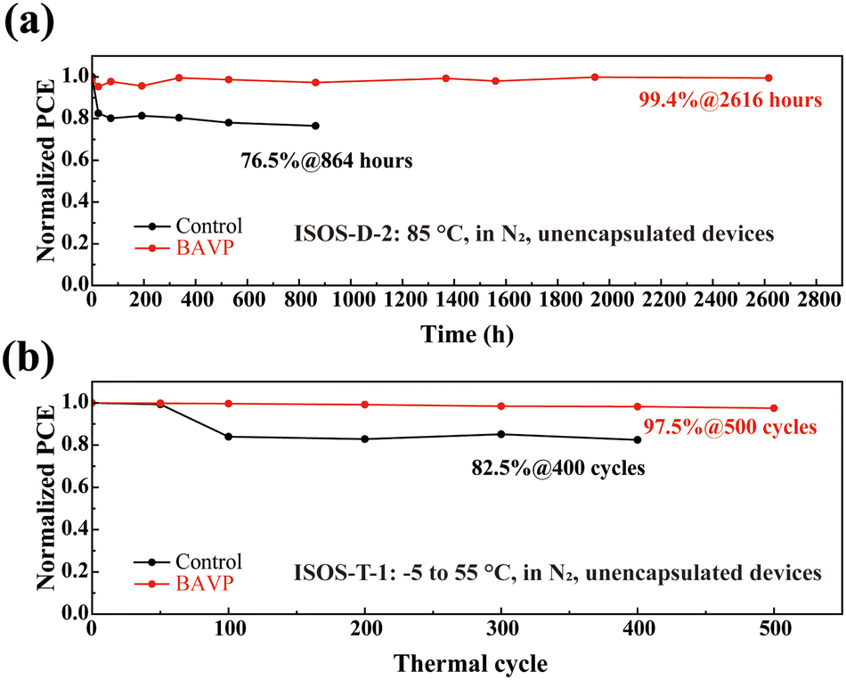 | ||
| Fig. 5 (a) Thermal stability test of the unencapsulated PSCs at 85 °C in N2 following the ISOS-D-2 protocol. (b) Thermal-cycling stability test of the unencapsulated PSCs at a temperature range of −5 to 55 °C in N2 following the ISOS-T-1 protocol. | ||
Conclusions
In conclusion, we successfully developed a BAVP strategy using PEA and EDA to address surface defects in blade-coated FAPbI3 perovskite films fabricated under ambient low-humidity conditions. By leveraging the complementary functionalities of these amines, this method effectively suppresses defect-induced recombination and optimizes energy-level alignment at the perovskite/C60 interface, significantly enhancing charge extraction. As a result, BAVP-treated PSCs achieved an impressive champion efficiency of 25.2%. Importantly, the unencapsulated devices exhibited remarkable thermal cycling stability, retaining 99.4% of their initial efficiency after 2616 hours at 85 °C in nitrogen following the ISOS-D-2 protocol, and 97.5% after 500 thermal cycles (−5 to 55 °C) according to the ISOS-T-1 protocol. Additionally, owing to excellent surface uniformity achieved by the BAVP method, PSMs fabricated using the BAVP method delivered a high efficiency of 21.3% over a total area of 6.25 cm2, outperforming devices fabricated using traditional solution-based passivation methods (18.7%). Overall, this work highlights the BAVP strategy as a promising route towards high-performance, scalable, and durable perovskite photovoltaic devices, offering valuable insights for future research and commercialization efforts.Author contributions
C. Zhou, W. Fu and H. Chen developed the concept and designed the experiments. W. Fu and H. Chen supervised the project. C. Zhou and W. Wang carried out the experiments and performed device fabrication. H. Wu and Y. Zhou performed the PL, SCLC and EQE tests. J. Zhang and Y. Wang carried out the DFT calculations. G. Wu and Alex K.-Y. Jen commented on the paper. C. Zhou, W. Fu, and H. Chen wrote the paper. All authors discussed the results, and read and commented on the manuscript.Conflicts of interest
There are no conflicts to declare.Data availability
The data supporting this article have been included as part of the SI. The SI provides the experimental details and DFT calculation methods, the proposed reaction pathways, structural and morphological characterizations (XRD, SEM, AFM, GIXRD), energy-level and optical analyses (UPS, ESP, UV-vis, Tauc plots), photovoltaic parameters under forward and reverse scans, PCE statistics, operational stability data, and literature comparisons of device performance and stability. See DOI: https://doi.org/10.1039/d5ee04570c.Acknowledgements
This work was supported by the National Natural Science Foundation of China (grant no. 52472256), the Natural Science Foundation of Zhejiang Province (no. LD24E030002), the National Key Research and Development Program of China (no. 2024YFF1401100), and the Fundamental Research Funds for the Central Universities (226-2024-00005 and 226-2024-00056).Notes and references
- J. Park, J. Kim, H.-S. Yun, M. J. Paik, E. Noh, H. J. Mun, M. G. Kim, T. J. Shin and S. I. Seok, Nature, 2023, 616, 724 CrossRef CAS.
- J. Du, J. Chen, B. Ouyang, A. Sun, C. Tian, R. Zhuang, C. Chen, S. Liu, Q. Chen, Z. Li, X. Wu, J. Cai, Y. Zhao, R. Li, T. Xue, T. Cen, K. Zhao and C.-C. Chen, Energy Environ. Sci., 2025, 18, 3196–3210 RSC.
- G. Kim, H. Min, K. S. Lee, D. Y. Lee, S. M. Yoon and S. I. Seok, Science, 2020, 370, 108 CrossRef CAS PubMed.
- J. Jeong, M. Kim, J. Seo, H. Lu, P. Ahlawat, A. Mishra, Y. Yang, M. A. Hope, F. T. Eickemeyer, M. Kim, Y. J. Yoon, I. W. Choi, B. P. Darwich, S. J. Choi, Y. Jo, J. H. Lee, B. Walker, S. M. Zakeeruddin, L. Emsley, U. Rothlisberger, A. Hagfeldt, D. S. Kim, M. Grätzel and J. Y. Kim, Nature, 2021, 592, 381 CrossRef CAS.
- W. Peng, K. Mao, F. Cai, H. Meng, Z. Zhu, T. Li, S. Yuan, Z. Xu, X. Feng, J. Xu, M. D. McGehee and J. Xu, Science, 2023, 379, 683 CrossRef CAS PubMed.
- Z. Li, X. Sun, X. Zheng, B. Li, D. Gao, S. Zhang, X. Wu, S. Li, J. Gong, J. M. Luther, Z. Li and Z. Zhu, Science, 2023, 382, 284 CrossRef CAS.
- “Best Research-Cell Efficiency Chart,” Available online: https://www.nrel.gov/pv/cell-efficiency.html, Accessed 6th August 2025.
- S. S. Sangale, H. Son, S. W. Park, P. Patil, T. K. Lee, S.-N. Kwon and S.-I. Na, Adv. Mater., 2025, 37, 2420093 CrossRef CAS.
- K. K. Shin Thant, C. Seriwattanachai, T. Jittham, N. Thamangraksat, P. Sakata and P. Kanjanaboos, Adv. Energy Mater., 2025, 15, 2403088 CrossRef CAS.
- Z. Yang, W. Zhang, S. Wu, H. Zhu, Z. Liu, Z. Liu, Z. Jiang, R. Chen, J. Zhou, Q. Lu, Z. Xiao, L. Shi, H. Chen, L. K. Ono, S. Zhang, Y. Zhang, Y. Qi, L. Han and W. Chen, Sci. Adv., 2021, 7, eabg3749 CrossRef CAS.
- S. Yu, Z. Xiong, H. Zhou, Q. Zhang, Z. Wang, F. Ma, Z. Qu, Y. Zhao, X. Chu, X. Zhang and J. You, Science, 2023, 382, 1399 CrossRef CAS.
- Y. Huang, X. Lei, T. He, Y. Jiang and M. Yuan, Adv. Energy Mater., 2022, 12, 2100690 CrossRef CAS.
- S. Sun, A. Tiihonen, F. Oviedo, Z. Liu, J. Thapa, Y. Zhao, N. T. P. Hartono, A. Goyal, T. Heumueller, C. Batali, A. Encinas, J. J. Yoo, R. Li, Z. Ren, I. M. Peters, C. J. Brabec, M. G. Bawendi, V. Stevanovic, J. Fisher and T. Buonassisi, Matter, 2021, 4, 1305 CrossRef CAS.
- S. Masi, A. F. Gualdrón-Reyes and I. Mora-Seró, ACS Energy Lett., 2020, 5, 1974 CrossRef CAS.
- C. Fu, Z. Gu, Y. Tang, Q. Xiao, S. Zhang, Y. Zhang and Y. Song, Angew. Chem., Int. Ed., 2022, 61, e202117067 CrossRef CAS PubMed.
- C. Li, X. Wang, E. Bi, F. Jiang, S. M. Park, Y. Li, L. Chen, Z. Wang, L. Zeng, H. Chen, Y. Liu, C. R. Grice, A. Abudulimu, J. Chung, Y. Xian, T. Zhu, H. Lai, B. Chen, R. J. Ellingson, F. Fu, D. S. Ginger, Z. Song, E. H. Sargent and Y. Yan, Science, 2023, 379, 690 CrossRef CAS.
- Z. Yang, J. Dou, S. Kou, J. Dang, Y. Ji, G. Yang, W.-Q. Wu, D.-B. Kuang and M. Wang, Adv. Funct. Mater., 2020, 30, 1910710 CrossRef CAS.
- H. Liu, T. Liu, X. Wang, G. Hu, B. Zheng, X. Yu, Y. Wang and D. Yang, Adv. Energy Mater., 2024, 14, 2401809 CrossRef CAS.
- M. Wang, Z. Shi, C. Fei, Z. J. D. Deng, G. Yang, S. P. Dunfield, D. P. Fenning and J. Huang, Nat. Energy, 2023, 8, 1229 CrossRef CAS.
- D. P. McMeekin, G. Sadoughi, W. Rehman, G. E. Eperon, M. Saliba, M. T. Hörantner, A. Haghighirad, N. Sakai, L. Korte, B. Rech, M. B. Johnston, L. M. Herz and H. J. Snaith, Science, 2016, 351, 151 CrossRef CAS PubMed.
- C. Yi, J. Luo, S. Meloni, A. Boziki, N. Ashari-Astani, C. Grätzel, S. M. Zakeeruddin, U. Röthlisberger and M. Grätzel, Energy Environ. Sci., 2016, 9, 656 RSC.
- K. Zhang, Y. Wang, M. Tao, L. Guo, Y. Yang, J. Shao, Y. Zhang, F. Wang and Y. Song, Adv. Mater., 2023, 35, 2211593 CrossRef CAS PubMed.
- S. Shan, Y. Zhou, C. Xu, G. You, H. Chen, W. Fu, L. Zuo and H. Chen, Small, 2025, 21, 2410172 CrossRef CAS.
- A. I. A. Soliman, Y. Zhang, L. Zhang, H. Wu, S. Shan, Y. Zhou, C. Xu, W. Fu and H. Chen, Adv. Funct. Mater., 2025, 35, 2412886 CrossRef CAS.
- G. Qu, S. Cai, Y. Qiao, D. Wang, S. Gong, D. Khan, Y. Wang, K. Jiang, Q. Chen, L. Zhang, Y.-G. Wang, X. Chen, A. K.-Y. Jen and Z.-X. Xu, Joule, 2024, 8, 2123 CrossRef CAS.
- Y.-H. Lin, V. Vikram, F. Yang, X.-L. Cao, A. Dasgupta, R. D. J. Oliver, A. M. Ulatowski, M. M. McCarthy, X. Shen, Q. Yuan, M. G. Christoforo, F. S. Y. Yeung, M. B. Johnston, N. K. Noel, L. M. Herz, M. S. Islam and H. J. Snaith, Science, 2024, 384, 767 CrossRef CAS.
- M. I. Haider, H. Hu, T. Seewald, S. Ahmed, M. Sultan, L. Schmidt-Mende and A. Fakharuddin, Sol. RRL, 2023, 7, 2201092 CrossRef CAS.
- Z. Zhang, M. A. Kamarudin, A. K. Baranwal, G. Kapil, S. R. Sahamir, Y. Sanehira, M. Chen, L. Wang, Q. Shen and S. Hayase, Angew. Chem., Int. Ed., 2022, 61, e202210101 CrossRef CAS PubMed.
- C. Liu, Y. Yang, H. Chen, J. Xu, A. Liu, A. S. R. Bati, H. Zhu, L. Grater, S. S. Hadke, C. Huang, V. K. Sangwan, T. Cai, D. Shin, L. X. Chen, M. C. Hersam, C. A. Mirkin, B. Chen, M. G. Kanatzidis and E. H. Sargent, Science, 2023, 382, 810 CrossRef CAS PubMed.
- Y. Huang, K. Yan, B. Niu, Z. Chen, E. Gu, H. Liu, B. Yan, J. Yao, H. Zhu, H. Chen and C.-Z. Li, Energy Environ. Sci., 2023, 16, 557 RSC.
- W. Feng, X. Liu, G. Liu, G. Yang, Y. Fang, J. Shen, B. Jin, X. Chen, Y.-H. Huang, X.-D. Wang, C. Wu, S. Yang and W.-Q. Wu, Angew. Chem., Int. Ed., 2024, 63, e202403196 CrossRef CAS PubMed.
- Z. Ren, Z. Cui, X. Shi, L. Wang, Y. Dou, F. Wang, H. Lin, H. Yan and S. Chen, Joule, 2023, 7, 2894 CrossRef CAS.
- Y. Deng, X. Zheng, Y. Bai, Q. Wang, J. Zhao and J. Huang, Nat. Energy, 2018, 3, 560 CrossRef CAS.
- H. Hu, D. B. Ritzer, A. Diercks, Y. Li, R. Singh, P. Fassl, Q. Jin, F. Schackmar, U. W. Paetzold and B. A. Nejand, Joule, 2023, 7, 1574 CrossRef CAS.
- R. Ahmed, S. Rehman, Z. Chen, F. Ye and X. Ren, Angew. Chem., Int. Ed., 2025, 64, e202418763 CrossRef CAS PubMed.
- S. Xiong, F. Tian, F. Wang, A. Cao, Z. Chen, S. Jiang, D. Li, B. Xu, H. Wu, Y. Zhang, H. Qiao, Z. Ma, J. Tang, H. Zhu, Y. Yao, X. Liu, L. Zhang, Z. Sun, M. Fahlman, J. Chu, F. Gao and Q. Bao, Nat. Commun., 2024, 15, 5607 CrossRef CAS.
- Q. Jiang, J. Tong, Y. Xian, R. A. Kerner, S. P. Dunfield, C. Xiao, R. A. Scheidt, D. Kuciauskas, X. Wang, M. P. Hautzinger, R. Tirawat, M. C. Beard, D. P. Fenning, J. J. Berry, B. W. Larson, Y. Yan and K. Zhu, Nature, 2022, 611, 278 CrossRef CAS PubMed.
- Y. Pan, J. Wang, Z. Sun, J. Zhang, Z. Zhou, C. Shi, S. Liu, F. Ren, R. Chen, Y. Cai, H. Sun, B. Liu, Z. Zhang, Z. Zhao, Z. Cai, X. Qin, Z. Zhao, Y. Ji, N. Li, W. Huang, Z. Liu and W. Chen, Nat. Commun., 2024, 15, 7335 CrossRef CAS.
- Y. Zhou, X. Huang, J. Zhang, L. Zhang, H. Wu, Y. Zhou, Y. Wang, Y. Wang, W. Fu and H. Chen, Adv. Energy Mater., 2024, 14, 2400616 CrossRef CAS.
- C. Luo, G. Zheng, X. Wang, F. Gao, C. Zhan, X. Gao and Q. Zhao, Energy Environ. Sci., 2023, 16, 178 RSC.
- A. Al-Ashouri, A. Magomedov, M. Roß, M. Jošt, M. Talaikis, G. Chistiakova, T. Bertram, J. A. Márquez, E. Köhnen, E. Kasparavičius, S. Levcenco, L. Gil-Escrig, C. J. Hages, R. Schlatmann, B. Rech, T. Malinauskas, T. Unold, C. A. Kaufmann, L. Korte, G. Niaura, V. Getautis and S. Albrecht, Energy Environ. Sci., 2019, 12, 3356 RSC.
- Y. Zhou, Y. Zhang, L. Zhang, H. Wu, Y. Zhou, X. Xu, J. Yu, X. Wu, J. Xie, W. Fu, G. Wu and H. Chen, Adv. Funct. Mater., 2024, 34, 2408774 CrossRef CAS.
- S. Yuan, D. Zheng, T. Zhang, Y. Wang, F. Qian, L. Wang, X. Li, H. Zheng, Z. Diao, P. Zhang, T. Pauporté and S. Li, Nat. Commun., 2025, 16, 2052 CrossRef CAS PubMed.
- Y. Li, Y. Yan, Y. Fu, W. Jiang, M. Liu, M. Chen, X. Huang, G. Lu, X. Lu, J. Yin, S. Wu and A. K.-Y. Jen, Angew. Chem., Int. Ed., 2024, 63, e202412515 CrossRef CAS.
- L. Tan, H. Jiang, R. Yang, L. Shen, C. Sun, Y. Jin, X. Guan, P. Song, L. Zheng, C. Tian, L. Xie, J. Yang and Z. Wei, Adv. Energy Mater., 2024, 14, 2400549 CrossRef CAS.
- L. Yang, Y. Jin, Z. Fang, J. Zhang, Z. Nan, L. Zheng, H. Zhuang, Q. Zeng, K. Liu, B. Deng, H. Feng, Y. Luo, C. Tian, C. Cui, L. Xie, X. Xu and Z. Wei, Nano-Micro Lett., 2023, 15, 111 CrossRef CAS.
- H. Wu, X. Lian, S. Tian, Y. Zhang, M. Qin, Y. Zhang, F. Wang, X. Lu, G. Wu and H. Chen, Sol. RRL, 2020, 4, 2000087 CrossRef CAS.
Footnote |
| † C. Zhou, W. Wang and H. Wu contributed equally to this work. |
| This journal is © The Royal Society of Chemistry 2025 |