
 Open Access Article
 This Open Access Article is licensed under a
 Creative Commons Attribution 3.0 Unported Licence
Exposing binding-favourable facets of perovskites for tandem solar cells†
Junke
Wang‡
 *a,
Shuaifeng
Hu‡
a,
Zehua
Chen‡
b,
Zhongcheng
Yuan
a,
Pei
Zhao
ac,
Akash
Dasgupta
a,
Fengning
Yang
a,
Jin
Yao
d,
Minh Anh
Truong
e,
Gunnar
Kusch
f,
Esther Y-H.
Hung
a,
Nick R. M.
Schipper
g,
Laura
Bellini
g,
Guus J. W.
Aalbers
g,
Zonghao
Liu
hi,
Rachel A.
Oliver
f,
Atsushi
Wakamiya
e,
René A. J.
Janssen
g and
Henry J.
Snaith
*a
*a,
Shuaifeng
Hu‡
a,
Zehua
Chen‡
b,
Zhongcheng
Yuan
a,
Pei
Zhao
ac,
Akash
Dasgupta
a,
Fengning
Yang
a,
Jin
Yao
d,
Minh Anh
Truong
e,
Gunnar
Kusch
f,
Esther Y-H.
Hung
a,
Nick R. M.
Schipper
g,
Laura
Bellini
g,
Guus J. W.
Aalbers
g,
Zonghao
Liu
hi,
Rachel A.
Oliver
f,
Atsushi
Wakamiya
e,
René A. J.
Janssen
g and
Henry J.
Snaith
*a
aClarendon Laboratory, Department of Physics, University of Oxford, Parks Road, Oxford OX1 3PU, UK. E-mail: junke.wang@physics.ox.ac.uk; henry.snaith@physics.ox.ac.uk
bBeijing Computational Science Research Center, Beijing 100193, China
cResearch Center for Computational Science, Institute for Molecular Science, Okazaki 444-8585, Japan
dNational Thin Film Cluster Facility for Advanced Functional Materials, Department of Physics, University of Oxford, Parks Road, Oxford OX1 3PU, UK
eInstitute for Chemical Research, Kyoto University, Gokasho, Uji, Kyoto 611-0011, Japan
fDepartment of Materials Science and Metallurgy, University of Cambridge, Cambridge, UK
gMolecular Materials and Nanosystems and Institute for Complex Molecular Systems, Eindhoven University of Technology, P.O. Box 513, 5600 MB, Eindhoven, The Netherlands
hWuhan National Laboratory for Optoelectronics, Huazhong University of Science and Technology (HUST), Wuhan, China
iHubei Optics Valley Laboratory, Wuhan, China
First published on 2nd July 2025
Abstract
Improved understanding of heterojunction interfaces has enabled multijunction photovoltaic devices to achieve power conversion efficiencies that exceed the detailed-balance limit for single-junctions. For wide-bandgap perovskites, however, the pronounced energy loss across the heterojunctions of the active and charge transport layers impedes multijunction devices from reaching their full efficiency potential. Here we find that for polycrystalline perovskite films with mixed-halide compositions, the crystal termination—a factor influencing the reactivity and density of surface sites—plays a crucial role in interfacial passivation for wide-bandgap perovskites. We demonstrate that by templating the growth of polycrystalline perovskite films toward a preferred (100) facet, we can reduce the density of deep-level trap states and enhance the binding of modification ligands. This leads to a much-improved heterojunction interface, resulting in open-circuit voltages of 1.38 V for 1.77-eV single-junction perovskite solar cells. In addition, monolithic all-perovskite double-junction solar cells achieve open-circuit voltage values of up to 2.22 V, with maximum power point tracking efficiencies reaching 28.6% and 27.7% at 0.25 and 1.0 cm2 cell areas, respectively, along with improved operational and thermal stability at 85 °C. This work provides universally applicable insights into the crystalline facet-favourable surface modification of perovskite films, advancing their performance in optoelectronic applications.
Broader contextAll-perovskite tandem solar cells offer a promising pathway to achieve higher solar power conversion efficiencies compared to existing single-junction solar cells, combined with the advantage of low-temperature processing. However, they have not yet achieved their full performance potential, mainly due to a substantial open-circuit voltage deficit and poor operational stability in wide-bandgap perovskites. Previous studies have attributed significant performance losses to non-radiative recombination at the interface between wide-bandgap perovskites and the electron transport layer. In this study, we demonstrate that for polycrystalline perovskite films with mixed-halide compositions, the crystal termination plays a crucial role in interfacial passivation for wide-bandgap perovskites. The atomic arrangements of as-deposited polycrystalline perovskite films can impact the formation of surface defect states and the binding strength with passivation ligands, ultimately controlling the non-radiative recombination process at the perovskite heterojunctions. Assisted by theoretical calculations, we utilise ammonium-based salts to template the growth of the polycrystalline perovskite films towards a favourable termination. This results in a low trap density and strong binding with passivation ligands. This approach significantly reduces interfacial losses and enhances the output voltage in wide-bandgap and all-perovskite tandem solar cells. |
Introduction
Metal-halide perovskite-based tandem solar cells offer a promising avenue to achieving power conversion efficiencies (PCEs) of over 45%1 with low embodied energy and potential for mass production. Thanks to the recent development of wide-bandgap (∼1.8 eV)2 and narrow-bandgap (∼1.2 eV)3 perovskite photo-absorbers, “all-perovskite” tandems have demonstrated PCEs of over 30%,4 surpassing by a significant margin those reported in the single-junction counterparts5 and approaching the realised performance of “perovskite-on-silicon” tandem solar cells.6The key to maximising the performance of tandems lies in minimising the energetic losses in each sub-cell.1,3,7 This is achieved by reducing non-radiative recombination losses at the heterojunction interfaces and controlling detrimental trap states in the absorber layer.8,9 For narrow-bandgap (∼1.25 eV) tin–lead (Sn–Pb) perovskites, effective bulk and interface modifications have enabled single-junction perovskite solar cells (PSCs) with open-circuit voltage (VOC) deficits – the difference between the bandgap energy and the VOC – of about 0.35 eV.10–15 In comparison, solar cells with a bandgap of over 1.75 eV have yet to achieve VOC deficits below 0.40 eV.16,17 Therefore, improving the VOC of wide-bandgap (>1.75 eV) sub-cells and tandem performance remains an imperative and challenging task in the field.
For “positive–intrinsic–negative” (p–i–n) wide-bandgap PSCs, the most significant performance loss has been attributed to the perovskite and electron-transporting-layer (ETL) interface.18–20 Most mitigation strategies developed for the interface can be categorised as suppressing electronic defects and introducing field-effect interlayers between the perovskite and ETL.19,21–23 Conceivably, their effectiveness relies on binding passivation materials to the perovskite surface, where specific crystal terminations can determine the density and reactivity of surface sites.24,25 Previously, organic molecules, including ammonium-based ligands, have been found to influence the crystallographic orientation of hybrid perovskites, when added into the perovskite precursor solution.26,27 Furthermore, numerous recent studies have reported advancements in promoting a preferred orientation, which helps control trap density and enhance the phase stability of perovskite materials.16,28–32 However, research focusing on orientation-dependent interface modifications remains limited, despite the fact that the binding of ligands to the perovskite surface will strongly depend upon the termination of the target surface. Further exploration of these aspects could provide viable pathways for optimising perovskite devices and minimising voltage losses.
Here, we investigate the effect of interface modification for wide-bandgap PSCs with respect to the perovskite crystal orientation and surface termination. Our investigations start by analysing the impact of atomic coordination on surface-defect formation and binding strength of passivation ligands using first-principles calculations. We identify that a (100)-dominated crystal growth of perovskite material shows the lowest trap density and substantially reduced interfacial losses when in contact with a top ETL. This leads to a photoluminescence quantum yield (PLQY) of up to 4.3% for the 1.77 eV perovskites when incorporated into the complete device stack. Through optimisation, we fabricate single-junction PSCs with VOC values of up to 1.38 V, demonstrating a deficit of 0.39 eV at the corresponding bandgap. We proceed to fabricate two-terminal all-perovskite tandems, achieving the VOC values of 2.22 V and maximum power point tracked (MPPT) PCEs of up to 28.6% at 0.25-cm2 devices. With the active area increased to 1 cm2, the cells exhibit a slight performance gap compared to smaller cells, yielding PCE values of up to 27.7% (certified at 25.96%).
Facet engineering
We first consider the atomic arrangement and surface states of halide perovskites. For a cubic ABX3 perovskite, the (100) crystal orientations provide a stacking sequence of atomic layers ⋯AX–BX2–AX–BX2⋯, the (110) has a stacking sequence of ⋯X2–ABX–X2–ABX–X2⋯, and the (111) possesses a stacking pattern of ⋯AX3–B–AX3–B–AX3⋯. These distinct atomic arrangements lead to pristine (100), (110), and (111) facets with six possible surface terminations in total, i.e., the AX (100) and BX2 (100), and the X2 (110), ABX (110), AX3 (111), and B (111) (Fig. 1a). Using density functional theory (DFT) calculations for the archetype FAPbBr3 (FA = formamidinium) perovskite, we show that the (100) terminations are non-polar and do not introduce new states in the bandgap. In contrast, the (110) and (111) terminations exhibit electronic states with an extra positive or negative charge, depending on the atomic arrangement at the surface (Fig. 1b). This increases susceptibility for surface-defect formation with energies near the Fermi level in the perovskites with (110) and (111) orientations, in comparison to those with (100) surfaces.27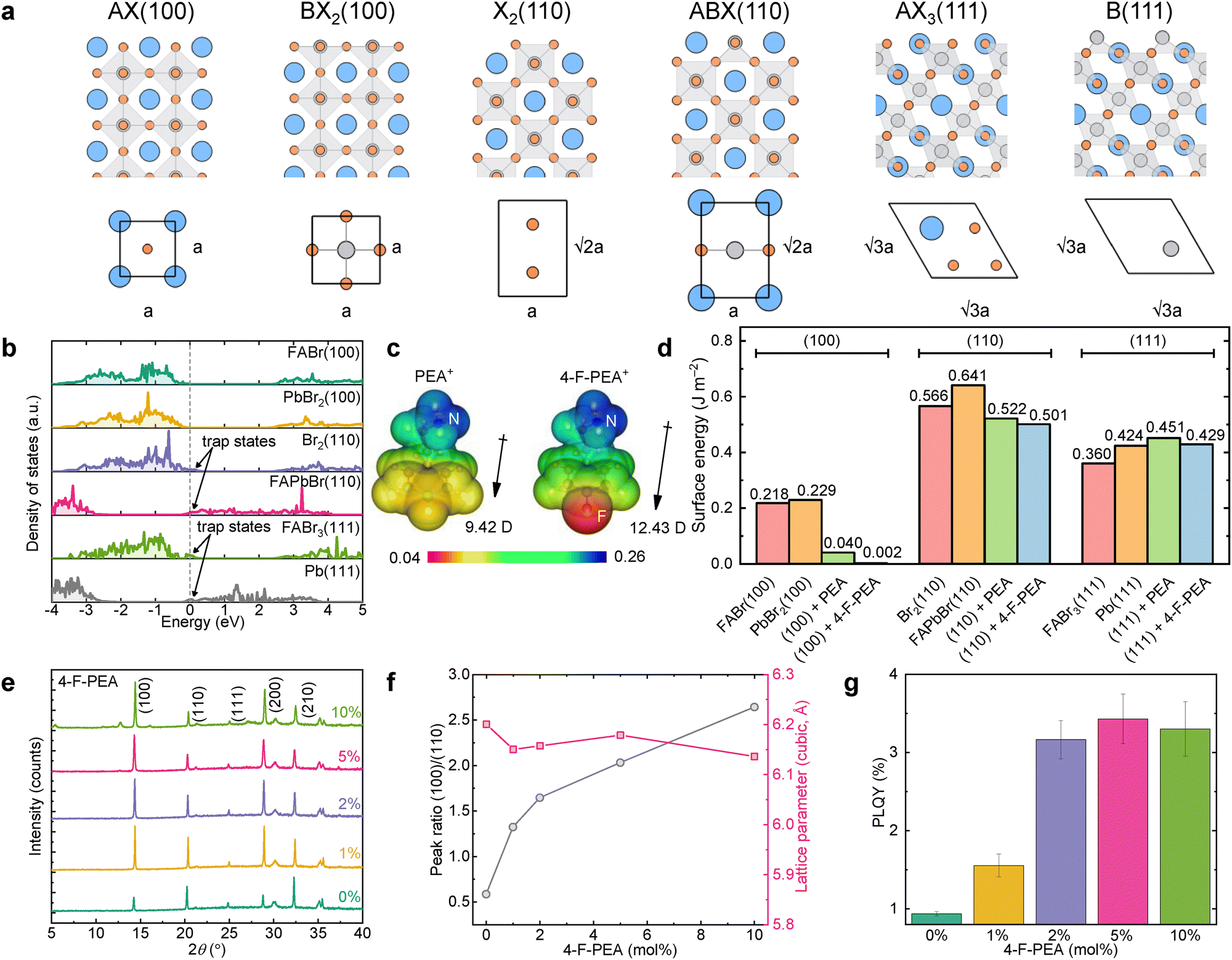 | ||
| Fig. 1 Surface atomic arrangements and crystal growth of wide-bandgap perovskites. (a), Cross-sectional and top-view of the structural models of the slabs for (100), (110), and (111) surfaces as created from cubic metal-halide perovskite ABX3 (A, blue; B, grey; X, orange). Here, ‘a’ is the lattice constant of the cubic ABX3. (b), Calculated density of states for FABr (100), PbBr2 (100), Br2 (110), FAPbBr (110), FABr3 (111), and Pb (111) surfaces. The Fermi energy level is set to zero. (c), Calculated electrostatic potentials (a.u.) of PEA and 4-F-PEA cations. (d), Surface energies of (100), (110), and (111) surfaces considering without and with the treatment of PEA or 4-F-PEA. (e), XRD patterns, (f), cubic lattice parameters and (100)/(110) peak ratios, and (g), PLQY values at a 1-sun equivalent intensity (data are mean ± s.d.), of wide-bandgap perovskite thin films at varying 4-F-PEA concentrations (0–10 mol%). | ||
To enable perovskite growth with lower trap densities, we seek ligands that effectively interact with perovskite species for crystal nucleation and enhance the (100) orientation by reducing its surface energy. As depicted in Fig. 1c, phenethylammonium (PEA) and 4-fluoro-phenethylammonium (4-F-PEA) cations have considerably larger dipole moments (9.42 and 12.43 Debye, respectively) than the FA cation (0.22 Debye), favouring stronger interactions with perovskite precursors (Fig. S1 and Table S1, ESI†).33 Furthermore, the higher maximum electrostatic potential on the –NH3+ side of 4-F-PEA suggests an increased binding strength with the PbX3− network.34 This aligns with our DFT calculations for the archetype FAPbBr3 perovskite (Fig. 1d), where we replace the outermost FA cation with either a PEA or a 4-F-PEA cation at the FABr (100), FAPbBr (110), and FABr3 (111) slabs (Methods). We find that the presence of PEA and 4-F-PEA additives considerably reduces the surface energy of the neutral (100)-orientated perovskite, with 4-F-PEA resulting in the lowest surface energy. In contrast, the additive treatment has minimal effects on the surface energy of crystals with both the (110) and (111) orientations. Therefore, we expect 4-F-PEA to stabilise Br-containing perovskites with a preferred exposure of the (100) crystal facets.
Using ligands with preferential crystallographic interactions is a common approach to control the shape of nano- and macro-crystals during colloidal growth.35,36 To assess the impact of 4-F-PEA on the crystal growth of wide-bandgap perovskites, the additive is introduced into the precursor solution with an initial composition of Cs0.2FA0.8Pb(I0.6Br0.4)3. The X-ray diffraction (XRD) pattern of the as-annealed untreated (reference) film displays major reflections at 14.4°, 20.3°, and 25.0° that are attributed to (100), (110), and (111) planes, respectively, for a 40% Br-containing perovskite (Fig. 1e).37 The initial peak intensity ratio of (100)/(110) in the reference film is smaller than 1, but this increases to 2.6 with the addition of 10 mol% 4-F-PEA into the perovskite precursor. This indicates a reorientation of (100) planes parallel with the substrate plane. Grazing-incidence wide-angle X-ray scattering (GIWAXS) patterns confirm this observation, displaying an increased peak intensity near q = 1.0 Å−1 in the out-of-plane direction (χ = 0°) for the 4-F-PEA-treated film (Fig. S2, ESI†).38 We also observe that the summed peak area of (100), (110), and (111) planes increases with the 4-F-PEA addition, suggesting an increased film crystallinity upon the additive treatment (Table S2, ESI†). No discernible 2D phase formation is observed up to 5 mol% of 4-F-PEA addition, indicating minimal incorporation of cations into the perovskite lattice (Fig. 1f and Fig. S3, ESI†). Time-of-flight secondary ion mass spectroscopy (ToF-SIMS) results suggest that residual PEA-based cations are primarily located within the top (∼100 nm) region of the perovskite film (Fig. S4, ESI†). This confirms the role of PEA ligands in templating crystal growth from the exposed top surface during crystallisation.39 Our evaluation of the optoelectronic properties of the modified perovskite films, through PLQY analysis, shows a more than three-fold increase in the 4-F-PEA added samples (up to 3.4%) compared with the reference film (0.94%) (Fig. 1g). This suggests that either the enhanced (100) crystal orientation and crystallinity reduce the trap density of perovskite films, or that the residual 4-F-PEA coated surfaces are well passivated, or a combination of both, thanks to the as-designed molecular modification.
Facet-enhanced surface passivation and phase stability
Interface passivation is critical to suppressing non-radiative recombination losses across the wide-bandgap perovskite/charge-transport-layer heterojunctions. This can be achieved by reducing deep trap states at the interface or physically decoupling the electronic interaction between the perovskite and charge transport layers19—strategies that favour a strong binding between the passivation material and perovskite interfaces.24,25,40 In this analysis, we utilise a bimolecular ethane-1,2-diammonium (EDA)/phenethylammonium (PEA) ligand modification, given the high device VOCs reported for this passivation ligand pair.11,41,42 To understand the passivation of EDA/PEA ligands in more detail, we consider their interactions with defect sites (e.g., VFA− or BrPb3−) on the six possible terminal surfaces of (100), (110), and (111) crystal orientations (Fig. 1a and Fig. S5, ESI†). We find that EDA/PEA ligands show the highest coverage and binding affinity on a (100)-terminated surface, followed by (110) and (111) terminations (Fig. 2a). On an intrinsically benign (100) surface, introducing antisite defect BrPb3−—the most common defect with low formation energy in Br-containing perovskite films9—causes localised deep traps that are dominated by only Br-s/-p states (Fig. 2b and c). This contrasts with other typical defects, e.g., VBr+, VFA−, BrFA2−, and VPb2−, that do not generate deep traps (Fig. S6, ESI†). After passivation, we find that BrPb3−-generated deep traps are eliminated, primarily through the charge transfer process between the EDA/PEA ligands and the (100) perovskite surface (Fig. 2b, c and Fig. S7, ESI†). Interestingly, on both (110) and (111) surfaces, we observe that the EDA/PEA ligands are not able to passivate all the surface states (Fig. S8, ESI†). Therefore, our computational study provides reassurance that enabling a (100)-preferred orientation also favours interface passivation of wide-bandgap perovskite materials. | ||
| Fig. 2 Termination-dependent passivation and nanoscale optical properties for wide-bandgap perovskite interface. (a) Calculated binding energy and coverage of PEA/EDA ligands on (100), (110), and (111) surfaces. The more negative binding energy indicates a stronger ligand adhesion. The coverage of ligands is defined as 1/a2, where a2 is the area of the (1 × 1) (100) surface displayed in Fig. 1a. (b and c) Calculated projected density of states (PDOS) for FABr (100) (b) and PbBr2 (100) (c) surfaces. Top, pristine surface; middle, surface with a BrPb3− antisite defect; bottom, surface passivated by PEA+ and EDA2+ cations. The deep trap states that appeared in the bandgap are indicated by arrows. States related to organic molecules are not shown as they have low contributions near the band edges. The Fermi energy level is set to zero. (d), PLQY of wide-bandgap perovskites processed on glass and covered by an ETL (ETL stack) and in a p–i–n stack, with (cross-hatched) or without (open) PEA/EDA surface passivation. The stars represent calculated QFLS (eV) given the average PLQY values. (e and f), Top-view SEM images (e) and CL hyperspectral imaging with a spectral window of 650–800 nm (f) of reference and 4-F-PEA (1 mol%) perovskite films with and without e-beam-induced phase separation. (g), The corresponding CL line-scan spectra for arrows shown in (f). Green dashed line, reference film; orange dashed line, 4-F-PEA film. The scale bars are 500 nm. | ||
We verify the impact of crystal orientation on interface passivation using PLQY analysis (Fig. 2d). For the reference film covered with a [6,6]-phenyl-C61-butyric acid methyl ester (PCBM) ETL, we observe a relatively small improvement in PLQY (from 0.02 to 0.14%) following EDA/PEA passivation. In comparison, the PLQY of the 4-F-PEA sample increases by nearly two orders of magnitude (from 0.04 to 2.89%) after passivating the perovskite/ETL interface, which corresponds to a projected 112-meV increase in quasi-Fermi level splitting (QFLS). Notably, without passivation, the relatively low PLQY of the 4-F-PEA sample (0.04%) suggests that the improvement in bulk crystallinity resulting from the additive treatment (Table S2, ESI†) does not substantially enhance the perovskite/ETL interface. Additionally, we observe minimal differences in PLQY between surface-passivated perovskites on either bare glass or NiOx/(2-(4-(bis(4-methoxyphenyl)amino)phenyl)-1-cyanovinyl)phosphonic acid (MPA-CPA)43 as the hole transport layer (HTL) (Fig. S9a–c, ESI†), suggesting that surface treatments similarly affect the bulk characteristics of the perovskite prior to depositing an ETL. Besides reducing interfacial defects, we infer that enhanced ligand coverage can suppress non-radiative recombination losses by reducing the contact area between the perovskite and ETL.19,44 We also observe a similar enhancement in PLQY within a complete p–i–n stack, where the 4-F-PEA sample exhibits a threefold increase in PLQY (4.30%) compared with the reference sample (1.21%). This corresponds to a calculated QFLS of 1.41 and 1.37 eV for the 4-F-PEA and reference device, respectively. We note that it is surprising that the passivated complete p–i–n stack (without electrode) exhibits higher PLQYs than the passivated perovskite/ETL stack processed on glass, yet for the non-passivated reference and 4-F-PEA films, the PLQY values are similar. We interpret these observations to suggest that passivation may also positively influence the buried interface, resulting in the HTL/perovskite interface being less lossy than the glass/perovskite interface. This aligns with our findings of a notable PLQY enhancement after passivating the reference and 4-F-PEA films processed on HTLs (Fig. S9a and b, ESI†). The trends in PLQY can be well reproduced across samples from different batches (Fig. S9d, ESI†). We propose that the solution- and annealing-based post-treatment facilitates the recrystallisation of the perovskite films,11,45 altering crystal orientation and globally improving film crystallinity. This further contributes to reducing non-radiative recombination losses at the interface (Fig. S10, ESI†). In summary, our findings indicate that a well-oriented (100) crystal surface in the perovskite film leads to a significantly better-passivated perovskite/ETL interface.
In wide-bandgap perovskites with over 20% Br at the X-site, phase heterogeneity incurred during film growth or device operation has been found to negatively impact the performance and stability of photovoltaic devices.8,46 We postulate that the crystal reorientation facilitated by our additive treatment helps to immobilise halide anions and enhance material stability. To probe the phase stability, we combine secondary electron (SE) and cathodoluminescence (CL) microscopy to visualise the microscopic optoelectronic properties of perovskite films (Fig. 2e–g). The hyperspectral dataset shows that initially both the reference and 4-F-PEA (1 mol%) films are homogeneous by displaying a wide-bandgap perovskite emission peaked near 680 nm (Fig. S11, ESI†). No discernible CL emissions from either low-energy (∼750 nm, iodide-rich perovskite47) or high-energy (∼520 nm for PbI248 and ∼600 nm for 85% Br-rich perovskite49) phases can be identified (Fig. S12, ESI†). During extended CL measurements, we find a substantial transition of CL emission peaks from 680 to 750 nm in the reference sample, which can be attributed to electron-beam-induced iodide segregation.50 In comparison, the 4-F-PEA sample appears to be more robust against beam-induced halide segregation. The trend in phase stability is also verified using time-dependent PL spectra (Fig. S13, ESI†). The higher intensity in 690 ± 40 nm filtered CL map suggests an unchanged wide-bandgap phase in the 4-F-PEA film, as opposed to the brighter 760 ± 20 nm filtered CL map for the degraded reference film (Fig. S12b and c, ESI†). Notably, for beam-induced halide segregation, we observe higher emission intensity at grain boundaries relative to grain interiors, similar to those observed for light-induced ion migration in wide-bandgap perovskite materials.51 Additionally, CL hyperspectral imaging reveals considerably higher uniformity in the emission wavelength for the 4-F-PEA film, which is characterised by a single peak at 688.5 ± 6.2 nm (Fig. 2f–g and Fig. S14, ESI†). In contrast, the reference sample displays an inhomogeneous phase distribution, evidenced by a double peak at 683.1 ± 5.2 and 746.6 ± 11.6 nm. Therefore, we conclude that facet engineering also enhances the phase stability of wide-bandgap perovskite materials.
Single-junction solar cells
By leveraging these insights, we fabricate 4-F-PEA-treated Cs0.2FA0.8Pb(I0.6Br0.4)3 PSCs in a p–i–n structure of fluorinated tin oxide (FTO)/NiOx/MPA-CPA/perovskite/PCBM/polyethyleneimine (PEI)/SnOx/Ag (Fig. S15, ESI†). The device statistics suggest a substantial increase in VOC and PCE values after treating the perovskite film with 1–2 mol% of 4-F-PEA, resulting in a maximum steady-state efficiency of 20.5% in the 4-F-PEA-treated device with an active area of 0.25 cm2 (Fig. 3a and Fig. S16, S17, ESI†). These devices feature a maximum VOC of 1.38 V, enabling a deficit of 0.39 V compared to the 1.77 eV photovoltaic bandgap (Fig. S18, ESI†). The electroluminescence external quantum efficiency (EL–EQE) for reference and 4-F-PEA device show EQE values of 0.15 and 1.8% under an injection current around the short-circuit current density (JSC), 18.5 mA cm−2. This increase from 0.15 to 1.8% translates to a 60-meV reduction in the non-radiative recombination loss (ΔVOC,nr) and a calculated VOC of 1.38 V for the 4-F-PEA device, in good agreement with the measured cell data (Fig. 3b). Additionally, the high-sensitivity EQE spectrum suggests slightly reduced sub-bandgap states for the 4-F-PEA device (Fig. S19, ESI†).52,53 As discussed in the PLQY analysis, we believe that the performance improvement mainly arises from a better-passivated perovskite/ETL interface rather than the bulk of the perovskite itself. We also performed PL imaging under open-circuit (OC) and short-circuit (SC) conditions, to visualise the spatial distribution of luminescence and determine the “charge collection quality” (QColl) for full devices (Fig. 3d).54 At OC the 4-F-PEA and reference device exhibit a mean QFLS value (calculated from the absolute PL intensity) of 1.37 and 1.35 eV, respectively, suggesting an enhanced perovskite/ETL interface over millimetre length scale for the 4-F-PEA-treated device (Fig. 3e). When comparing the QFLS at SC and OC conditions,54 we observed that the 4-F-PEA device displays an overall higher collection quality than the reference device, with the average values increasing from 0.989 to 0.992. | ||
| Fig. 3 Photovoltaic performance and stability of wide-bandgap PSCs. (a) The J–V characteristics of champion single-junction solar cell measured under simulated AM1.5G illumination (100 mW cm−2) in reverse and forward sweeps. The inset shows the PCE after 30 s of MPPT. (b) EL–EQE vs. current density for representative reference and 4-F-PEA single-junction PSCs. A dotted line is drawn where the injected current density is approximate to the JSC under 1-sun illumination. (c) The PCE (determined by MPPT, measured periodically under AM1.5G 1-sun irradiance at room temperature) vs. time for reference and 4-F-PEA single-junction solar cells aged at 85 °C in the dark in N2. A dotted horizontal line is drawn to indicate when the device PCE dropped to 80% of its initial performance. (d), QFLS (measured at OC in complete devices) and charge collection quality (Qcoll, by comparing the QFLS measured at the device OC and SC) maps for reference and 4-F-PEA PSCs (Methods), measured after 0 h (fresh) and 2100 h of 85 °C dark ageing in N2. The scale bars are 1 mm. (e), The corresponding QFLS histograms of reference and 4-F-PEA devices before and after ageing. | ||
To test the thermal stability of cells, we measure the MPP efficiency of reference and 4-F-PEA-treated devices at various time intervals, during ageing at 85 °C in N2 (ISOS-D-2).55 The reference device drops its initial performance to below 80% within 100 h, while the best 4-F-PEA-treated device retains around 80% of its initial PCE after 1000 h (Fig. 3c). QFLS mapping over millimetre length scales reveals that the 4-F-PEA devices maintain a 15-meV higher mean QFLS than the reference cells after ageing at 85 °C for 2100 h (Fig. 3d). Interestingly, the aged reference device exhibits a much lower average QColl value (0.39) compared with the aged 4-F-PEA device (0.52). These results, in line with the superior JSC and fill factor (FF) data measured for the 4-F-PEA cell (Fig. S20, ESI†), demonstrate the better current collection quality of the 4-F-PEA-treated devices after thermal stressing. Additionally, we expose encapsulated solar cells to full-spectrum simulated sunlight (∼76 mW cm−2) at 85 °C under OC in ambient air (ISOS-L-2). This stringent ageing condition results in rapidly decreased cell performance for both types of devices within the first 100 h of exposure (T80 lifetime < 48 h, Fig. S21, ESI†). Analyses of the photovoltaic (PV) parameters suggest a rapid decrease in both JSC and FF during ageing, indicating the formation of resistive barriers for charge-carrier extraction. Despite that, the 4-F-PEA devices constantly display higher PCEs than the reference during the tracking period. Examining the cross-sectional morphology after about 240 h of ageing shows that the 4-F-PEA-treated cell largely retains its initial grain morphology, in contrast to the “merged grain morphology” observed in the reference (Fig. S22, ESI†). This suggests that the modification enhances the stability of the PSCs under temperature and light-soaking conditions. We hypothesise that a stronger bonding affinity between the perovskite surface and the EDA/PEA passivator may contribute to the maintained performance after ageing (Fig. S23, ESI†). We anticipate that further investigations into stable passivation ligands and additives will be beneficial in enhancing long-term operational stability.40
Tandem solar cells
We fabricate monolithic all-perovskite tandem solar cells comprising 1.77 eV wide-bandgap and 1.26 eV narrow-bandgap Cs0.1FA0.6MA0.3Pb0.5Sn0.5I3 (MA = methylammonium) absorbers based on a device structure shown in Fig. 4a. The sub-cells are connected through a PCBM/PEI/SnOx/indium zinc oxide (IZO)/poly(3,4-ethylene dioxythiophene):polystyrene (PEDOT:PSS) charge extraction and recombination interconnecting layer. The champion tandem devices, enabled by the high-quality 4-F-PEA-treated wide-bandgap sub-cell and narrow-bandgap perovskite from our previous studies (Fig. S24, ESI†),14 exhibit a steady-state PCE of 28.6 and 27.7% (25.96% certified by the Japan Advanced Institute of Science and Technology (AIST)) with an aperture area of 0.25 and 1 cm2, respectively (Fig. 4b and Fig. S25, S26 (ESI†), and Table 1). The statistical performance data suggest good reproducibility of the tandem cells, with the 4-F-PEA-treated devices featuring a maximum VOC of 2.22 V (Fig. S27, ESI†). We note that our multi-source solar simulator is adjusted to achieve low mismatch factors (<1%) for both sub-cells, adding credibility to our cell data measured in-house (Fig. S28, ESI†).56 To analyse the efficiency potential of tandem solar cells, we measure injection current-dependent absolute EL spectra for both sub-cells integrated into a tandem (Fig. S29, ESI†).18 The reconstructed pseudo-J–V curves imply a VOC of 0.883 and 1.330 V for the narrow- and wide-bandgap sub-cell, respectively, suggesting a summed tandem VOC of 2.213 V, which is very close to the measured data under simulated AM1.5 sunlight (2.217 V). This indicates negligible VOC losses incurred in the recombination junction (Fig. 4c). By simply reducing the series resistance losses in the tandem cell, we would be able to achieve a high FF (89.9%) and a PCE of 32.5%, as inferred from our pseudo-J–V curve. Furthermore, optical simulations suggest that a tandem JSC of ∼17.1 mA cm−2 can be achieved after eliminating parasitic absorption (such as that from PEDOT:PSS) and matching the JSC of the sub-cells. Consequently, the reconstructed pseudo-J–V curves indicate a practical PCE of 33.6%, upon further realising the 95% VOC for both sub-cells (Fig. S30, ESI†). | ||
| Fig. 4 Photovoltaic performance of all-perovskite tandem solar cells. (a) Device configuration and cross-sectional SEM of tandem solar cells. The scale bar is 1 μm. (b) The J–V characteristics of champion tandem solar cells measured with an aperture area of 0.25 or 1.00 cm2. The inset shows the PCE after 30 s of MPPT. (c) Reconstructed or pseudo J–V characteristics of wide- and narrow-bandgap sub-cell obtained from the EL–EQE vs. injection current density curves and scaled to the short-circuit photocurrent density (16.3 mA cm−2) according to the measured tandem solar cell. The reconstructed tandem J–V characteristics are obtained by adding the voltage of both sub-cells at each current density. (d) MPP tracking stability of an encapsulated device in ambient air at room temperature under simulated AM1.5G 1-sun illumination. (e) The MPP efficiency of tandem solar cells measured periodically under AM1.5G 1-sun irradiance at room temperature, aged at 85 °C in the dark in N2 for the length of time shown on the x-axis. | ||
| Cells | Device area (cm2) | Scan directiona | V OC (V) | J SC (mA cm−2) | FF | PCE (%) | Steady-state PCE (%) |
|---|---|---|---|---|---|---|---|
| a Rev. and Fwd. represent reverse (VOC to JSC) and forward (JSC to VOC) J–V scan directions, respectively. | |||||||
| Double-junction | 0.25 | Rev. | 2.19 | 16.4 | 0.81 | 29.0 | 28.6 |
| Fwd. | 2.18 | 16.4 | 0.79 | 28.1 | |||
| 1 | Rev. | 2.18 | 16.6 | 0.77 | 28.0 | 27.7 | |
| Fwd. | 2.18 | 16.5 | 0.75 | 27.0 | |||
We test the operating stability of tandem devices under continuous MPP tracking under simulated AM1.5G 1-sun illumination in ambient air at room temperature. The device retains 85% of its initial PCE after 460 hours of continuous operation (Fig. 4d). When stored at 85 °C in N2 (ISOS-D-2), the best cell maintains around 80% of its initial performance after 900 hours, while on average, tandem devices show a T70 for about 300 hours (Fig. 4e and Fig. S31, ESI†). This result is comparable to that of single-junction wide-bandgap devices (Fig. 3c). However, when encapsulated tandem cells are aged under full-spectrum sunlight illumination with an intensity of ∼76 mW cm−2 at the OC and 85 °C in ambient air (ISOS-L-2), their performance drops rapidly within just a few hours (T80 lifetime <5 h, Fig. S32, ESI†). This accelerated degradation is primarily due to the additional interfaces created by the two perovskite absorbers. We expect that the combined effects of heat and photocarrier/ion accumulation at the perovskite interfaces can dramatically reduce the material stability, especially in the narrow-bandgap sub-cell.17 Further investigations of contact materials resilient to heat and light stressors are paramount to boosting the more realistic operational stability of tandem solar cells for outdoor applications.
Conclusions
We have presented a thorough investigation of the generally overlooked crystal-facet-dependent trap states and interface modification for wide-bandgap perovskite materials. We identified that the atomic coordination of the (100) surfaces is more favourable than the other perovskite orientations in achieving low defect density and high binding strength of passivation ligands at the perovskite and charge transport layer heterojunctions. Controlling the film growth towards (100) orientation resulted in more stable wide-bandgap PSCs with high VOC values and all-perovskite tandem solar cells with low energetic losses. Our study shed light on viable strategies for improving the properties of perovskites and their photovoltaic devices.We consider that mixed-halide, MA-free wide-bandgap perovskites tend to form a substantial fraction of (110) crystal facets, even though (100) orientations are thermodynamically more stable. We reason that due to the complex crystallisation dynamics of mixed halide species, the fabrication protocol can lead to very different crystal orientations in perovskite films with nearly equal iodide and bromide compositions. Therefore, we believe it is crucial to study the relationship between crystal growth and interfacial non-radiative recombination losses for similar perovskite compositions (e.g., 40–60% Br content), as this is essential for enhancing the performance of muljunction solar cells.
In this study, we show that controlling crystal growth towards (100) terminations can reduce surface defect formation and improve the binding of PEA/EDA passivation ligands. While we acknowledge that enhancing the effectiveness of surface passivation depends on both the control of crystal facets and the molecular design of passivation ligands, this optimisation approach is generally applicable to perovskites with varying compositions and bandgaps.
Methods
Materials
Unless stated, all materials were used as received without further purification. Pre-patterned glass/FTO substrates (10 Ω sq−1) were purchased from AGC Inc. CsI (99.99%), SnI2 (99.99%), SnF2 (99%), Sn powder (<45 μm, 99.8%), ammonium thiocyanate (NH4SCN, 99.99%), SnF2 (99.99%), C60 pyrrolidine tris-acid (97%), Al2O3 nanoparticles (<50 μm, 20 wt% in isopropanol), PEI solution (Mn ∼60![[thin space (1/6-em)]](https://www.rsc.org/images/entities/char_2009.gif) 000, 50 wt% in H2O), and all anhydrous solvents including N,N-dimethylformamide (DMF, 99.8%), dimethyl sulfoxide (DMSO, ≥99.9%), isopropanol (99.5%), ethanol (≥99.5%), chlorobenzene (CB, 99.8%), anisole (99.7%) were purchased from Sigma-Aldrich. PbI2 (>98%), PbBr2 (>98%), PbCl2 (>98%), [4-(3,6-Dimethyl-9H-carbazol-9-yl)butyl]phosphonic acid (Me-4PACz, >99.0%), piperazine (anhydrous, >98.0%) and glycine hydrochloride (>99.0%) were purchased from TCI Chemicals. MPA-CPA was purchased from Dyenamo AB. Formamidinium iodide (FAI), methylammonium iodide (MAI), ethane-1,2-diammonium iodide (EDAI2), ethane-1,2-diammonium bromide (EDABr2), phenethylammonium iodide (PEAI), phenethylammonium bromide (PEABr), phenethylammonium chloride (PEACl) and 4-fluoro-phenethylammonium chloride (4-F-PEACl) were purchased from Greatcell Solar Materials. PC61BM was purchased from Nano-C. C60 (99.99%, sublimed) was purchased from ATR Company. PEDOT:PSS (Al4083) was purchased from Heraeus Clevios. NiOx nanoparticles (2.5 wt%, ethanol) were purchased from Avantama. IZO sputtering target was purchased from Testbourne.
000, 50 wt% in H2O), and all anhydrous solvents including N,N-dimethylformamide (DMF, 99.8%), dimethyl sulfoxide (DMSO, ≥99.9%), isopropanol (99.5%), ethanol (≥99.5%), chlorobenzene (CB, 99.8%), anisole (99.7%) were purchased from Sigma-Aldrich. PbI2 (>98%), PbBr2 (>98%), PbCl2 (>98%), [4-(3,6-Dimethyl-9H-carbazol-9-yl)butyl]phosphonic acid (Me-4PACz, >99.0%), piperazine (anhydrous, >98.0%) and glycine hydrochloride (>99.0%) were purchased from TCI Chemicals. MPA-CPA was purchased from Dyenamo AB. Formamidinium iodide (FAI), methylammonium iodide (MAI), ethane-1,2-diammonium iodide (EDAI2), ethane-1,2-diammonium bromide (EDABr2), phenethylammonium iodide (PEAI), phenethylammonium bromide (PEABr), phenethylammonium chloride (PEACl) and 4-fluoro-phenethylammonium chloride (4-F-PEACl) were purchased from Greatcell Solar Materials. PC61BM was purchased from Nano-C. C60 (99.99%, sublimed) was purchased from ATR Company. PEDOT:PSS (Al4083) was purchased from Heraeus Clevios. NiOx nanoparticles (2.5 wt%, ethanol) were purchased from Avantama. IZO sputtering target was purchased from Testbourne.
Solar cell fabrication
Glass/FTO substrates (3 × 3 cm2) were cleaned sequentially in soapy water, deionized water, acetone and 2-propanol by sonication and UV ozone. To prepare 1.77 eV PSCs, NiOx nanoparticles (1:10 diluted in ethanol, v:v) and MPA-CPA (1 mg mL−1 in ethanol) were sequentially spin-coated at 3000 rpm for 30 s with an acceleration of 1000 rpm s−1. The HTLs were annealed together at 100 °C for 10 min. To improve the wetting of perovskite inks, Al2O3 nanoparticles (1:150 diluted in isopropanol, v:v) were spin-coated at 4000 rpm for 30 s with an acceleration of 2000 rpm s−1 and annealed at 100 °C for 2 min. The Cs0.2FA0.8Pb(I0.6Br0.4)3 precursor solution was prepared by dissolving stoichiometric CsI (0.2), FAI (0.8), PbI2 (0.4), and PbBr2 (0.6) salts in mixed DMF:DMSO solvent (4:1, v:v) at a concentration of 1.2 M in 1 hour before the deposition. 200 μL precursor solution was cast on the HTL at 4000 rpm for 32 s with an acceleration of 1000 rpm s−1, and 150 μL anisole was dropped on the spinning substrate 8 s before the end of the program. The perovskite film was annealed at 100 °C for 15 min. For the additive treatment, 1–10 mol% 4-F-PEACl was added to the precursor solution, in which the FAI content was reduced correspondingly. After cooling down, PEA/EDA passivation solution (mixing 1 mg PEAI and PEABr and 0.5 mg EDAI2:EDABr2 in 1 mL isopropanol while keeping a I:Br molar ratio of 6:4) was spin-coated on top at 4000 rpm for 30 s with an acceleration of 2000 rpm s−1, followed by annealing at 100 °C for 5 min. The ETL PCBM solution (15 mg mL−1 in CB) was spin-coated at 1000 rpm for 30 s with an acceleration of 1000 rpm s−1. To facilitate the growth of SnOx on PCBM, a seeding PEI layer (0.025 wt% diluted in isopropanol) was spin-coated at 4000 rpm for 30 s with an acceleration of 2000 rpm s−1. This is followed by depositing a 20 nm SnOx using temporal atomic-layer-deposition (ALD) at 100 °C and a 100 nm Ag (0.1 Å s−1 for the first 10 nm and 1 Å s−1 for the next 90 nm) top contact using thermal evaporation.
To prepare tandem solar cells, the same processing conditions were used for the wide-bandgap sub-cell until the SnOx layer. A 10 nm sputter-coated IZO layer was deposited to enhance the conductivity of the tandem recombination junction. A shadow mask with aperture areas slightly larger than the device active area was used to avoid additional shunt losses. To prepare the narrow-bandgap perovskite sub-cell, the HTL PEDOT:PSS solution was filtered by a 0.45 μm PVDF filter and spin-coated on the IZO at 1000 rpm for 10 s and 5000 rpm for 30 s in air. Then, the substrates were annealed in air at 105 °C for 10 min and another 10 min in an N2-filled glovebox 1 hour before the deposition of mixed Sn–Pb perovskite layer. The precursor solution Cs0.1FA0.6MA0.3Pb0.5Sn0.5I3 was prepared by dissolving stoichiometric CsI (0.1), MAI (0.3), PbI2 (0.5), SnI2 (0.5), FAI (0.6), SnF2 (0.05), and NH4SCN (0.02) in mixed DMF and DMSO solvent (3:1, v:v) at a concentration of 1.9 M. Additionally, 2.5 mol% glycine hydrochloride11 and 0.5 mg mL−1 Sn powder57 were added into the precursor solution. The solution was dissolved at 45 °C for 40 min and filtered by 0.2 μm PTFE syringe filter before use. 200 μL precursor solution was cast on the PEDOT:PSS layer and spin-coated at 1000 rpm for 10 s (with an acceleration of 200 rpm s−1) and 4000 rpm for 40 s (with an acceleration of 1000 rpm s−1). 500 μL CB was dropped on the spinning substrate 20 seconds before the end of the program. The perovskite film was annealed at 100 °C for 10 min and 65 °C for over 10 min. After cooling down, a passivation solution mixed with piperazine and C60 pyrrolidine tris-acid was spin-coated dynamically, as reported previously.10 This is followed by depositing a 20 nm C60 ETL using thermal evaporation (0.1 Å s−1), a 20 nm ALD-SnOx, and a 100 nm Ag (0.1 Å s−1 for the first 10 nm and 1 Å s−1 for the next 90 nm) by thermal evaporation.
All devices were encapsulated for ageing tests using a cover glass and UV-cured adhesive (Eversolar AB-341, Everlight Chemical Industrial Co.) in a N2-filled glovebox. To improve the device stability at 85 °C in N2 (O2 < 10 ppm, H2O < 0.1 ppm) or under 85 °C in the ambient and full-spectrum illumination at the VOC, a 300 nm SiOx layer was sputter-coated58 on top of the device using a Cr (2.5 nm, 0.05 Å s−1)/Au (90 nm, 0.1 Å s−1) top contact.59
All the vacuum depositions were performed by the National Thin Film Cluster Facility (NTFC) for advanced functional materials, assembled by Angstrom Engineering and hosted by the University of Oxford. The thermal deposition chamber, sputter chamber, and ALD chamber are connected by handler units and sample transfer was performed under vacuum conditions.14 The SnOx process was performed using a Picosun (R200) ALD chamber at 5 mbar at 100 °C for the wide-bandgap sub-cell and 85 °C for the narrow-bandgap sub-cell. The tetrakis(dimethylamino) tin (iv) (TDMASn) and deionized (DI) water sources were heated to 75 and 25 °C with a pulse time of 1.4 and 1.6 s, respectively. The IZO layer was sputter-coated under 4 × 10⁻³ mbar using DC power with a pulse frequency of 20 kHz. The flow rates for Ar and O2 were 18 and 0.4 sccm during sputtering at room temperature. The SiOx layer was sputtered at room temperature under 4 × 10⁻³ mbar with an Ar flow rate of 18 sccm.
DFT calculations
To compare the energetics of (100), (110), and (111) surfaces of metal-halide perovskites in the presence of PEA or 4-F-PEA additive, we start from a periodic unit cell of cubic FAPbBr3. The cubic FAPbBr3 perovskite is considered as the prototypical example in this work due to its lower formation energy than its iodine counterpart.60 We then cleave the unit cell in [100], [110], and [111] directions. Depending on termination compositions, we obtain six (1 × 1) slab models, i.e., FABr (100), PbBr2 (100), Br2 (110), FAPbBr (110), FABr3 (111), and Pb (111), each one contains at least nine atomic layers. To avoid the spurious interaction between the periodic slabs via dipole–dipole interactions, the slabs are treated as symmetric with a vacuum region of >20 Å. The PEA or 4-F-PEA additive treatment in halide perovskite is modelled by replacing the outmost FA cation with a PEA or 4-F-PEA cation at the FABr (100), FAPbBr (110), and FABr3 (111) slabs. The inner three atomic layers of the perovskite slabs are fixed to mimic the bulk properties.To calculate the surface energy, we use the crystal cleaving and surface relaxation method,61,62 as given in detail in the ESI.† First-principles calculations are performed using the density functional theory as implemented in the Vienna ab initio simulation package (VASP).63 The electronic exchange–correlation interaction is described by the functional of Perdew–Burke–Ernzerhof (PBE) within the generalized gradient approximation (GGA).64 A plane-wave cutoff of 400 eV is used for all geometry optimisations. The D3 correction65 with Becke-Jonson damping is used to describe the van der Waals interactions. The convergence of the total energy and forces are considered within 10−5 eV and 0.02 eV Å−1, respectively. The Brillouin-zone integrations are performed using a Γ-centred k-point mesh with a grid spacing of 0.25 Å−1.
The binding energies (Eb) of EDA/PEA ligands with the perovskite surface are defined as Eb = Epvsk + Eligand − Eligand/pvsk, where Eligand/pvsk, Epvsk and Eligand are the total energies of the ligand-perovskite crystal system, the perovskite system after removing a ligand-halide compound (EDABr2/PEABr) and the ligand-halide compound, respectively. Here, the ligand–perovskite systems are taken from the snapshots of the ab initial molecular dynamics equilibrium simulations using the CP2K code.66 The atomic positions of these systems are optimized further by CP2K code at the ground state. The dipole moment of FA, PEA, and 4-F-PEA cations are calculated using the GAMESS,67 and the electrostatic potentials are visualized by Molekel 5.4.68 Crystal structures displayed in this work are visualized by VESTA.69
X-ray diffraction
1D-XRD was performed by a Panalytical X’Pert Pro X-ray diffractometer using a Cu Kα (1.5406 Å) source at 40 kV and 40 mA. The scan step size was 0.0167°, and the measurements were performed between 5–40°. To ensure similar film quality, all the perovskite films were processed on glass/indium tin oxide (ITO)/HTL substrates.PLQY analysis
A 532 nm continuous wave (CW) laser (ThorLabs DJ532-10) was used to excite the film samples through an optical fibre into an integrating sphere. The laser intensity was adjusted to 50 mW cm−2 (equivalent to 1 sun intensity for 1.77 eV bandgap). The emission spectra (three measurements per sample) were acquired by an optical fibre from the output of the integrating sphere to a QE Pro spectrometer. The QFLS values were determined according to QFLS = QFLSrad + kBT![[thin space (1/6-em)]](https://www.rsc.org/images/entities/i_char_2009.gif) ln(PLQE). The perovskite films were encapsulated to avoid the impact of the atmospheric environment.70
ln(PLQE). The perovskite films were encapsulated to avoid the impact of the atmospheric environment.70
CL hyperspectral mapping
CL hyperspectral maps were measured by an Attolight Allalin 4027 Chronos in CW mode at room temperature and high vacuum. The SE and CL images were acquired with an acceleration voltage of ∼3 kV and beam current of ∼63 pA, with 64 × 64-pixel resolution in a 3.0 μm field of view. Bandpass-filtered CL images were obtained by integrating CL intensities over specific energy ranges and analysed by a software package.71ToF-SIMS
Time-of-flight secondary ion mass spectrometry (ToF-SIMS) measurements were carried out using a M6 (IONTOF GmbH). A 30 keV Bi32+ primary ion beam with pulses width of 2.5 ns was used for data acquisition. During sputtering, a 10 keV Ar1200+ ion beam with a centre size of 1200 atoms was used. A low-energy flood gun was used for charge compensation. The raster area of the primary beam was 200 μm × 200 μm. In the ToF-SIMS experiments, Me-4PACz was used as the HTL, and an equivalent amount of PbCl2 was added along with PEACl and 4-F-PEACl (1 mol%). However, for other film and device characterisations, PbCl2 was omitted to prevent excess chloride from affecting the optical bandgap. It is also important to note that a small amount of PbCl2 (1 mol%) has minimal impact on device performance.SEM
SEM images were acquired by FEI Quanta 3D FEG microscopy. A 5 kV electron beam and secondary electron detector were used.EL–EQE spectra
EL–EQE spectra were measured using a home-built setup in an N2-filled glovebox at room temperature. A Keithley 2400 source meter unit (SMU) was used to drive the solar cells as LEDs, which are placed on the integrating sphere coupled with fibre and a spectrometer (Ocean Insight QE Pro) to collect the EL spectra. The system was calibrated by a standard halogen light source (HL-3P-INT-CAL) for absolute spectral response. Based on the EQE value of each sub-cell obtained at an injection current equal to the JSC under 1-sun illumination (EQEEL(JSC)), we calculated the voltage loss of the sub-cell using
QFLS imaging
A 450 nm LED (Thorlabs, M450LP1) was used to illuminate the PSCs from the glass side, which was electrically biased by a Keithley 2400 SMU. To determine the 1-sun illumination condition, the LED intensity was adjusted such that the JSC of the solar cell under analysis reaches a value similar to the J–V data. At VOC and JSC conditions, the luminescence images were measured by a camera (Andor Zyla 4.2 sCMOS sensor) and the PLQE and charge collection quality (QColl) were calculated using our previously reported method.54 For ageing tests, encapsulated solar cells using the Cr/Au contact are described above.Solar cell characterization
Both J–V and EQE measurements were performed in ambient air at room temperature. Wide-bandgap single-junction PSCs were measured without encapsulation unless otherwise stated. Tandem solar cells were encapsulated in N2 before measuring in air to avoid Sn oxidation. For J–V measurements, solar cells were illuminated under simulated AM1.5G irradiance generated by a Wavelabs SINUS-220 solar simulator (calibrated with a certified monocrystalline silicon solar cell, provided and certified by Fraunhofer ISE). A Keithley 2400 SMU was used to sweep the voltage from above VOC to below JSC in the reverse scan and from below JSC to above VOC in a forward scan at a scan rate of 300 mV s−1. To determine the steady state PCE, active MPP tracking using a gradient ascent algorithm was performed for 30 seconds. During the measurements, the devices were masked with a black shadow mask with an aperture area of 0.25 or 1 cm2. The mismatch factor was calculated to be less than 1% for both sub-cells.For the long MPP test (Fig. 4d), edge-encapsulated tandem solar cells (with Ag top contact) were measured in ambient under simulated AM1.5G illumination (Class ABA Newport solar simulator, LSH-7320) using a LabView MPP tracking script and a Keithley 2400 SMU. No UV filter was applied.
The EQE measurements were performed using a home-built setup. A modulated (Princeton Instruments SP2150) halogen lamp was used as the light source. The signal of solar cells was measured with a lock-in amplifier (Stanford Research, SR830) and transformed into EQE using a calibrated silicon reference cell. For tandem solar cells, a 850-nm LED bias light (Mightex Systems) and a bias voltage near the VOC of a narrow-bandgap sub-cell were used to measure the EQE response of the wide-bandgap sub-cell; whereas a 405-nm LED bias light (Mightex Systems) and a bias voltage near the VOC of a wide-bandgap sub-cell were used to measure the EQE response of the narrow-bandgap sub-cell. The JSC was obtained by integrating the EQE values with the AM1.5G spectrum according to
Author contributions
J. W. conceived the idea and planned the research. J. W. and S. H. fabricated the tandem solar cells. S. H. optimised and fabricated the narrow-bandgap perovskites. Z. C. performed the DFT calculation and analysis. Z. Y. performed the EL–EQE measurement and analysis. P. Z. discussed the theoretical results. A. D. measured the QFLS imaging and analysed the charge collection quality. F. Y. and E. Y.-H. H. performed the GIWAXS measurements and helped analyse the crystallographic data. J. Y. helped film depositions at NTCF. M. A. T. prepared the samples for ToF-SIMS measurements, A. W. supervised the project and provided the FTO substrates for solar cell experiments. G. K. and R. A. O. performed the CL measurements and helped with the data analysis. N. R. M. S., L. B., and G. J. W. A. helped fabricate wide-bandgap perovskite devices and performed sub-EQE analysis, and R. A. J. J. supervised the project. J. W., S. H., and Z. C. composed the initial draft. H. J. S. supervised the project and raised the grant funding for the laboratory infrastructure and research. All authors commented on it and contributed to improving the written manuscript.Conflicts of interest
H. J. S. is cofounder and CSO of Oxford PV Ltd. A. W. is co-founder and CSO of EneCoat Technologies Co., Ltd. All other authors declare no competing interests.Data availability
Data for this article are available at the Oxford University Research Archive, at https://ora.ox.ac.uk.Acknowledgements
This work was partly funded by the UK's Engineering and Physical Sciences Research Council (EPSRC) under grant numbers EP/S004947/1, EP/X038777/1, and EP/T028513/1, the UK Research and Innovation (UKRI) under the Horizon Europe guarantee funding under grant number 10054976 (The NEXUS project has received funding from the EU's Horizon Europe research and innovation program under grant agreement number 101075330, Views and opinions expressed are however those of the author(s) only and do not necessarily reflect those of the European Union or RIA) and the Marie Skłodowska Curie Actions Postdoc Fellow (UKRI Guarantee, grant numbers EP/Y029216/1 and EP/Y029135/1). Z. C. acknowledges funding from the National Natural Science Foundation of China (Grant 12404003). A. D. would like to thank the Penrose Scholarship for funding his studentship. E. Y.-H. H. would like to thank Xaar plc for funding her studentship. R. A. O. and G. K. acknowledge the CL-SEM grant from the EPSRC under EP/R025193/1. A. W. acknowledges the New Energy and Industrial Technology Development Organization (NEDO) and JST Mirai (JPMJMI22E2), KAKENHI (JP21H04699, JP24H00481), and International Collaborative Research Program of ICR, Kyoto University, for funding. P. Z. thanks for the financial support from the JSPS KAKENHI (JP24K17663). M. A. T. thanks for the financial support from the Grant-in-Aid for Scientific Research (B) (JP24K01571). Authors from the Eindhoven University of Technology acknowledge funding from HyET Solar Netherlands B.V., the EU's Horizon Europe research and innovation programme under grant agreement number 101075605 (SuPerTandem), the ERC (PERSTACK, 101098168), and the Dutch Research Council (NWO, Spinoza grant). We thank Dr Daichi Shirakura (Toray Research Center) for their assistance with the ToF-SIMS measurements. We thank the National Thin Film Cluster Facility for Advanced Functional Materials (NTCF) at the Department of Physics, University of Oxford, which has been funded by EPSRC (EP/M022900/1) and the Wolfson Foundation. We also thank H. Shimura, R. Yamaguchi and M. Yoshita from the Photovoltaic Calibration, Standards and Measurement Team, Renewable Energy Research Center (RENRC), National Institute of Advanced Industrial Science and Technology (AIST), Japan, for their kind support on our device calibration and M. Tetsuhiko (AIST) for the assistance with the device storage in Japan.References
- G. E. Eperon, M. T. Hörantner and H. J. Snaith, Metal halide perovskite tandem and multiple-junction photovoltaics, Nat. Rev. Chem., 2017, 1, 0095 CrossRef CAS.
- A. J. Ramadan, R. D. J. Oliver, M. B. Johnston and H. J. Snaith, Methylammonium-free wide-bandgap metal halide perovskites for tandem photovoltaics, Nat. Rev. Mater., 2023, 8, 822–838 CrossRef CAS.
- S. Hu, J. Thiesbrummel, J. Pascual, M. Stolterfoht, A. Wakamiya and H. J. Snaith, Narrow Bandgap Metal Halide Perovskites for All-Perovskite Tandem Photovoltaics, Chem. Rev., 2024, 124, 4079–4123 CrossRef CAS.
- M. A. Green, E. D. Dunlop, M. Yoshita, N. Kopidakis, K. Bothe, G. Siefer, X. Hao and J. Y. Jiang, Solar Cell Efficiency Tables (Version 65), Prog. Photovolt. Res. Appl., 2024, 33, 3–15 CrossRef.
- S. Liu, J. Li, W. Xiao, R. Chen, Z. Sun, Y. Zhang, X. Lei, S. Hu, M. Kober-Czerny, J. Wang, F. Ren, Q. Zhou, H. Raza, Y. Gao, Y. Ji, S. Li, H. Li, L. Qiu, W. Huang, Y. Zhao, B. Xu, Z. Liu, H. J. Snaith, N.-G. Park and W. Chen, Buried interface molecular hybrid for inverted perovskite solar cells, Nature, 2024, 632, 536–542 CrossRef.
- J. Liu, Y. He, L. Ding, H. Zhang, Q. Li, L. Jia, J. Yu, T. W. Lau, M. Li, Y. Qin, X. Gu, F. Zhang, Q. Li, Y. Yang, S. Zhao, X. Wu, J. Liu, T. Liu, Y. Gao, Y. Wang, X. Dong, H. Chen, P. Li, T. Zhou, M. Yang, X. Ru, F. Peng, S. Yin, M. Qu, D. Zhao, Z. Zhao, M. Li, P. Guo, H. Yan, C. Xiao, P. Xiao, J. Yin, X. Zhang, Z. Li, B. He and X. Xu, Perovskite/silicon tandem solar cells with bilayer interface passivation, Nature, 2024, 635, 596–603 CrossRef CAS.
- K. O. Brinkmann, P. Wang, F. Lang, W. Li, X. Guo, F. Zimmermann, S. Olthof, D. Neher, Y. Hou, M. Stolterfoht, T. Wang, A. B. Djurišić and T. Riedl, Perovskite–organic tandem solar cells, Nat. Rev. Mater., 2024, 9, 202–217 CrossRef CAS.
- J. Wang, L. Zeng, D. Zhang, A. Maxwell, H. Chen, K. Datta, A. Caiazzo, W. H. M. Remmerswaal, N. R. M. Schipper, Z. Chen, K. Ho, A. Dasgupta, G. Kusch, R. Ollearo, L. Bellini, S. Hu, Z. Wang, C. Li, S. Teale, L. Grater, B. Chen, M. M. Wienk, R. A. Oliver, H. J. Snaith, R. A. J. Janssen and E. H. Sargent, Halide homogenization for low energy loss in 2-eV-bandgap perovskites and increased efficiency in all-perovskite triple-junction solar cells, Nat. Energy, 2024, 9, 70–80 CrossRef CAS.
- X. Zheng, B. Chen, J. Dai, Y. Fang, Y. Bai, Y. Lin and H. Wei, Xiao C. Zeng and J. Huang, Defect passivation in hybrid perovskite solar cells using quaternary ammonium halide anions and cations, Nat. Energy, 2017, 2, 17102 CrossRef CAS.
- S. Hu, P. Zhao, K. Nakano, R. D. J. Oliver, J. Pascual, J. A. Smith, T. Yamada, M. A. Truong, R. Murdey, N. Shioya, T. Hasegawa, M. Ehara, M. B. Johnston, K. Tajima, Y. Kanemitsu, H. J. Snaith and A. Wakamiya, Synergistic Surface Modification of Tin–Lead Perovskite Solar Cells, Adv. Mater., 2023, 35, 2208320 CrossRef CAS.
- S. Hu, K. Otsuka, R. Murdey, T. Nakamura, M. A. Truong, T. Yamada, T. Handa, K. Matsuda, K. Nakano, A. Sato, K. Marumoto, K. Tajima, Y. Kanemitsu and A. Wakamiya, Optimized carrier extraction at interfaces for 23.6% efficient tin–lead perovskite solar cells, Energy Environ. Sci., 2022, 15, 2096–2107 RSC.
- Z. Zhang, R. Zhu, Y. Tang, Z. Su, S. Hu, X. Zhang, J. Zhang, J. Zhao, Y. Xue, X. Gao, G. Li, J. Pascual, A. Abate and M. Li, Anchoring Charge Selective Self-Assembled Monolayers for Tin–Lead Perovskite Solar Cells, Adv. Mater., 2024, 36, 2312264 CrossRef CAS.
- J. Tong, Q. Jiang, A. J. Ferguson, A. F. Palmstrom, X. Wang, J. Hao, S. P. Dunfield, A. E. Louks, S. P. Harvey, C. Li, H. Lu, R. M. France, S. A. Johnson, F. Zhang, M. Yang, J. F. Geisz, M. D. McGehee, M. C. Beard, Y. Yan, D. Kuciauskas, J. J. Berry and K. Zhu, Carrier control in Sn–Pb perovskites via 2D cation engineering for all-perovskite tandem solar cells with improved efficiency and stability, Nat. Energy, 2022, 7, 642–651 CrossRef CAS.
- S. Hu, J. Wang, P. Zhao, J. Pascual, J. Wang, F. Rombach, A. Dasgupta, W. Liu, M. A. Truong, H. Zhu, M. Kober-Czerny, J. N. Drysdale, J. A. Smith, Z. Yuan, G. J. W. Aalbers, N. R. M. Schipper, J. Yao, K. Nakano, S.-H. Turren-Cruz, A. Dallmann, M. G. Christoforo, J. M. Ball, D. P. McMeekin, K.-A. Zaininger, Z. Liu, N. K. Noel, K. Tajima, W. Chen, M. Ehara, R. A. J. Janssen, A. Wakamiya and H. J. Snaith, Steering perovskite precursor solutions for multijunction photovoltaics, Nature, 2024, 639, 93–101 CrossRef.
- C. Ge, Q. Xu, D. Liu, W. Ye, Y. Zhu, P. Zhang, J. Yang, G. Liang, L. Xu, Y. Zhou, H. Song, C. Chen and J. Tang, Light radiation annealing enables unidirectional crystallization of vacuum-assisted Sn–Pb perovskites for efficient tandem solar cells, Energy Environ. Sci., 2025, 18, 430–438 RSC.
- Z. Liu, R. Lin, M. Wei, M. Yin, P. Wu, M. Li, L. Li, Y. Wang, G. Chen, V. Carnevali, L. Agosta, V. Slama, N. Lempesis, Z. Wang, M. Wang, Y. Deng, H. Luo, H. Gao, U. Rothlisberger, S. M. Zakeeruddin, X. Luo, Y. Liu, M. Grätzel and H. Tan, All-perovskite tandem solar cells achieving >29% efficiency with improved (100) orientation in wide-bandgap perovskites, Nat. Mater., 2025, 24, 252–259 CrossRef CAS.
- J. Wang, B. Branco, W. H. M. Remmerswaal, S. Hu, N. R. M. Schipper, V. Zardetto, L. Bellini, N. Daub, M. M. Wienk, A. Wakamiya, H. J. Snaith and R. A. J. Janssen, Performance and stability analysis of all-perovskite tandem photovoltaics in light-driven electrochemical water splitting, Nat. Commun., 2025, 16, 174 CrossRef.
- J. Thiesbrummel, F. Peña-Camargo, K. O. Brinkmann, E. Gutierrez-Partida, F. Yang, J. Warby, S. Albrecht, D. Neher, T. Riedl, H. J. Snaith, M. Stolterfoht and F. Lang, Understanding and Minimizing VOC Losses in All-Perovskite Tandem Photovoltaics, Adv. Energy Mater., 2023, 13, 2202674 CrossRef CAS.
- J. Warby, F. Zu, S. Zeiske, E. Gutierrez-Partida, L. Frohloff, S. Kahmann, K. Frohna, E. Mosconi, E. Radicchi, F. Lang, S. Shah, F. Peña-Camargo, H. Hempel, T. Unold, N. Koch, A. Armin, F. De Angelis, S. D. Stranks, D. Neher and M. Stolterfoht, Understanding Performance Limiting Interfacial Recombination in pin Perovskite Solar Cells, Adv. Energy Mater., 2022, 12, 2103567 CrossRef CAS.
- M. Stolterfoht, P. Caprioglio, C. M. Wolff, J. A. Márquez, J. Nordmann, S. Zhang, D. Rothhardt, U. Hörmann, Y. Amir, A. Redinger, L. Kegelmann, F. Zu, S. Albrecht, N. Koch, T. Kirchartz, M. Saliba, T. Unold and D. Neher, The impact of energy alignment and interfacial recombination on the internal and external open-circuit voltage of perovskite solar cells, Energy Environ. Sci., 2019, 12, 2778–2788 RSC.
- D. Menzel, A. Al-Ashouri, A. Tejada, I. Levine, J. A. Guerra, B. Rech, S. Albrecht and L. Korte, Field Effect Passivation in Perovskite Solar Cells by a LiF Interlayer, Adv. Energy Mater., 2022, 12, 2201109 CrossRef CAS.
- T. Li, J. Xu, R. Lin, S. Teale, H. Li, Z. Liu, C. Duan, Q. Zhao, K. Xiao, P. Wu, B. Chen, S. Jiang, S. Xiong, H. Luo, S. Wan, L. Li, Q. Bao, Y. Tian, X. Gao, J. Xie, E. H. Sargent and H. Tan, Inorganic wide-bandgap perovskite subcells with dipole bridge for all-perovskite tandems, Nat. Energy, 2023, 8, 610–620 CrossRef CAS.
- J. Liu, M. De Bastiani, E. Aydin, G. T. Harrison, Y. Gao, R. R. Pradhan, M. K. Eswaran, M. Mandal, W. Yan, A. Seitkhan, M. Babics, A. S. Subbiah, E. Ugur, F. Xu, L. Xu, M. Wang, A. U. Rehman, A. Razzaq, J. Kang, R. Azmi, A. A. Said, F. H. Isikgor, T. G. Allen, D. Andrienko, U. Schwingenschlögl, F. Laquai and S. De Wolf, Efficient and stable perovskite-silicon tandem solar cells through contact displacement by MgFx, Science, 2022, 377, 302–306 CrossRef CAS.
- C. Ma, M.-C. Kang, S.-H. Lee, Y. Zhang, D.-H. Kang, W. Yang, P. Zhao, S.-W. Kim, S. J. Kwon, C.-W. Yang, Y. Yang and N.-G. Park, Facet-Dependent Passivation for Efficient Perovskite Solar Cells, J. Am. Chem. Soc., 2023, 145, 24349–24357 CrossRef CAS.
- C. Ma, M. Grätzel and N.-G. Park, Facet Engineering for Stable, Efficient Perovskite Solar Cells, ACS Energy Lett., 2022, 7, 3120–3128 CrossRef CAS.
- Y. Yu, R. Liu, C. Liu, X.-L. Shi, H. Yu and Z.-G. Chen, Synergetic Regulation of Oriented Crystallization and Interfacial Passivation Enables 19.1% Efficient Wide-Bandgap Perovskite Solar Cells, Adv. Energy Mater., 2022, 12, 2201509 CrossRef CAS.
- X. Zheng, Y. Hou, C. Bao, J. Yin, F. Yuan, Z. Huang, K. Song, J. Liu, J. Troughton, N. Gasparini, C. Zhou, Y. Lin, D.-J. Xue, B. Chen, A. K. Johnston, N. Wei, M. N. Hedhili, M. Wei, A. Y. Alsalloum, P. Maity, B. Turedi, C. Yang, D. Baran, T. D. Anthopoulos, Y. Han, Z.-H. Lu, O. F. Mohammed, F. Gao, E. H. Sargent and O. M. Bakr, Managing grains and interfaces via ligand anchoring enables 22.3%-efficiency inverted perovskite solar cells, Nat. Energy, 2020, 5, 131–140 CrossRef CAS.
- Z. Wu, Y. Zhao, C. Wang, T. Ma, C. Chen, Y. Liu, T. Jia, Y. Zhai, C. Chen, C. Zhang, G. Cao, Z. Yang, D. Zhao and X. Li, Enhancing Photovoltaically Preferred Orientation in Wide-Bandgap Perovskite for Efficient All-Perovskite Tandem Solar Cells, Adv. Mater., 2025, 37, 2412943 CrossRef CAS.
- D. Li, X. Sun, Y. Zhang, Z. Guan, Y. Yue, Q. Wang, L. Zhao, F. Liu, J. Wei and H. Li, Uniaxial-Oriented Perovskite Films with Controllable Orientation, Adv. Sci., 2024, 11, 2401184 CrossRef CAS.
- S. Qu, H. Huang, J. Wang, P. Cui, Y. Li, M. Wang, L. Li, F. Yang, C. Sun, Q. Zhang, P. Zhu, Y. Wang and M. Li, Revealing and Inhibiting the Facet-related Ion Migration for Efficient and Stable Perovskite Solar Cells, Angew. Chem., Int. Ed., 2025, 64, e202415949 CrossRef CAS.
- L. Wang, N. Wang, X. Wu, B. Liu, Q. Liu, B. Li, D. Zhang, N. Kalasariya, Y. Zhang, X. Yan, J. Wang, P. Zheng, J. Yang, H. Jin, C. Wang, L. Qian, B. Yang, Y. Wang, X. Cheng, T. Song, M. Stolterfoht, X. C. Zeng, X. Zhang, M. Xu, Y. Bai, F. Xu, C. Zhou and Z. Zhu, Highly Efficient Monolithic Perovskite/TOPCon Silicon Tandem Solar Cells Enabled by “Halide Locking”, Adv. Mater., 2025, 37, 2416150 CrossRef CAS.
- Y. Yao, B. Li, D. Ding, C. Kan, P. Hang, D. Zhang, Z. Hu, Z. Ni, X. Yu and D. Yang, Oriented wide-bandgap perovskites for monolithic silicon-based tandems with over 1000hours operational stability, Nat. Commun., 2025, 16, 40 CrossRef CAS.
- L. Xie, S. Du, J. Li, C. Liu, Z. Pu, X. Tong, J. Liu, Y. Wang, Y. Meng, M. Yang, W. Li and Z. Ge, Molecular dipole engineering-assisted strain release for mechanically robust flexible perovskite solar cells, Energy Environ. Sci., 2023, 16, 5423–5433 RSC.
- C. Liu, Y. Yang, H. Chen, J. Xu, A. Liu, A. S. R. Bati, H. Zhu, L. Grater, S. S. Hadke, C. Huang, V. K. Sangwan, T. Cai, D. Shin, L. X. Chen, M. C. Hersam, C. A. Mirkin, B. Chen, M. G. Kanatzidis and E. H. Sargent, Bimolecularly passivated interface enables efficient and stable inverted perovskite solar cells, Science, 2023, 382, 810–815 CrossRef CAS.
- E. J. W. Crossland, N. Noel, V. Sivaram, T. Leijtens, J. A. Alexander-Webber and H. J. Snaith, Mesoporous TiO2 single crystals delivering enhanced mobility and optoelectronic device performance, Nature, 2013, 495, 215–219 CrossRef CAS.
- C. X. Shan, Z. Liu and S. K. Hark, CdSe nanowires with controllable growth orientations, Appl. Phys. Lett., 2007, 90, 193123 CrossRef.
- D. P. McMeekin, G. Sadoughi, W. Rehman, G. E. Eperon, M. Saliba, M. T. Horantner, A. Haghighirad, N. Sakai, L. Korte, B. Rech, M. B. Johnston, L. M. Herz and H. J. Snaith, A mixed-cation lead mixed-halide perovskite absorber for tandem solar cells, Science, 2016, 351, 151–155 CrossRef CAS.
- M. Qin, P. F. Chan and X. Lu, A Systematic Review of Metal Halide Perovskite Crystallization and Film Formation Mechanism Unveiled by In Situ GIWAXS, Adv. Mater., 2021, 33, e2105290 CrossRef.
- S. Chen, X. Xiao, B. Chen, L. L. Kelly, J. Zhao, Y. Lin, M. F. Toney and J. Huang, Crystallization in one-step solution deposition of perovskite films: Upward or downward?, Sci. Adv., 2021, 7, eabb2412 CrossRef CAS.
- Y.-H. Lin, F. Yang, X.-L. Cao, A. Dasgupta, R. D. J. Oliver, A. M. Ulatowski, M. M. McCarthy, X. Shen, Q. Yuan, M. G. Christoforo, F. S. Y. Yeung, M. B. Johnston, N. K. Noel, L. M. Herz, M. S. Islam and H. J. Snaith, Bandgap-universal passivation enables stable perovskite solar cells with low photovoltage loss, Science, 2024, 384, 767–775 CrossRef CAS.
- Z. Wang, L. Zeng, T. Zhu, H. Chen, B. Chen, D. J. Kubicki, A. Balvanz, C. Li, A. Maxwell, E. Ugur, R. dos Reis, M. Cheng, G. Yang, B. Subedi, D. Luo, J. Hu, J. Wang, S. Teale, S. Mahesh, S. Wang, S. Hu, E. D. Jung, M. Wei, S. M. Park, L. Grater, E. Aydin, Z. Song, N. J. Podraza, Z.-H. Lu, J. Huang, V. P. Dravid, S. De Wolf, Y. Yan, M. Grätzel, M. G. Kanatzidis and E. H. Sargent, Suppressed phase segregation for triple-junction perovskite solar cells, Nature, 2023, 618, 74–79 CrossRef CAS.
- S. Hu, J. Pascual, W. Liu, T. Funasaki, M. A. Truong, S. Hira, R. Hashimoto, T. Morishita, K. Nakano, K. Tajima, R. Murdey, T. Nakamura and A. Wakamiya, A Universal Surface Treatment for p–i–n Perovskite Solar Cells, ACS Appl. Mater. Interfaces, 2022, 14, 56290–56297 CrossRef CAS.
- S. Zhang, F. Ye, X. Wang, R. Chen, H. Zhang, L. Zhan, X. Jiang, Y. Li, X. Ji, S. Liu, M. Yu, F. Yu, Y. Zhang, R. Wu, Z. Liu, Z. Ning, D. Neher, L. Han, Y. Lin, H. Tian, W. Chen, M. Stolterfoht, L. Zhang, W.-H. Zhu and Y. Wu, Minimizing buried interfacial defects for efficient inverted perovskite solar cells, Science, 2023, 380, 404–409 CrossRef CAS.
- W. H. M. Remmerswaal, B. T. van Gorkom, D. Zhang, M. M. Wienk and R. A. J. Janssen, Quantifying Non-Radiative Recombination in Passivated Wide-Bandgap Metal Halide Perovskites Using Absolute Photoluminescence Spectroscopy, Adv. Energy Mater., 2024, 14, 2303664 CrossRef CAS.
- J. Xue, R. Wang, K. L. Wang, Z. K. Wang, I. Yavuz, Y. Wang, Y. Yang, X. Gao, T. Huang, S. Nuryyeva, J. W. Lee, Y. Duan, L. S. Liao, R. Kaner and Y. Yang, Crystalline Liquid-like Behavior: Surface-Induced Secondary Grain Growth of Photovoltaic Perovskite Thin Film, J. Am. Chem. Soc., 2019, 141, 13948–13953 CrossRef CAS.
- K. Datta, S. C. W. van Laar, M. Taddei, J. Hidalgo, T. Kodalle, G. J. W. Aalbers, B. Lai, R. Li, N. Tamura, J. T. W. Frencken, S. V. Quiroz Monnens, R. J. E. Westbrook, D. J. Graham, C. M. Sutter-Fella, J.-P. Correa-Baena, D. S. Ginger, M. M. Wienk and R. A. J. Janssen, Local halide heterogeneity drives surface wrinkling in mixed-halide wide-bandgap perovskites, Nat. Commun., 2025, 16, 1967 CrossRef CAS.
- E. T. Hoke, D. J. Slotcavage, E. R. Dohner, A. R. Bowring, H. I. Karunadasa and M. D. McGehee, Reversible photo-induced trap formation in mixed-halide hybrid perovskites for photovoltaics, Chem. Sci., 2015, 6, 613–617 RSC.
- J. Ferrer Orri, E. M. Tennyson, G. Kusch, G. Divitini, S. Macpherson, R. A. Oliver, C. Ducati and S. D. Stranks, Using pulsed mode scanning electron microscopy for cathodoluminescence studies on hybrid perovskite films, Nano Express, 2021, 2, 024002 CrossRef CAS.
- H. Chen, A. Maxwell, C. Li, S. Teale, B. Chen, T. Zhu, E. Ugur, G. Harrison, L. Grater, J. Wang, Z. Wang, L. Zeng, S. M. Park, L. Chen, P. Serles, R. A. Awni, B. Subedi, X. Zheng, C. Xiao, N. J. Podraza, T. Filleter, C. Liu, Y. Yang, J. M. Luther, S. De Wolf, M. G. Kanatzidis, Y. Yan and E. H. Sargent, Regulating surface potential maximizes voltage in all-perovskite tandems, Nature, 2023, 613, 676–681 CrossRef CAS.
- H. Guthrey and J. Moseley, A Review and Perspective on Cathodoluminescence Analysis of Halide Perovskites, Adv. Energy Mater., 2020, 10, 1903840 CrossRef CAS.
- Y. Zhao, P. Miao, J. Elia, H. Hu, X. Wang, T. Heumueller, Y. Hou, G. J. Matt, A. Osvet, Y. T. Chen, M. Tarrago, D. de Ligny, T. Przybilla, P. Denninger, J. Will, J. Zhang, X. Tang, N. Li, C. He, A. Pan, A. J. Meixner, E. Spiecker, D. Zhang and C. J. Brabec, Strain-activated light-induced halide segregation in mixed-halide perovskite solids, Nat. Commun., 2020, 11, 6328 CrossRef CAS.
- G. J. W. Aalbers, T. P. A. van der Pol, K. Datta, W. H. M. Remmerswaal, M. M. Wienk and R. A. J. Janssen, Effect of sub-bandgap defects on radiative and non-radiative open-circuit voltage losses in perovskite solar cells, Nat. Commun., 2024, 15, 1276 CrossRef CAS.
- B. T. van Gorkom, T. P. A. van der Pol, K. Datta, M. M. Wienk and R. A. J. Janssen, Revealing defective interfaces in perovskite solar cells from highly sensitive sub-bandgap photocurrent spectroscopy using optical cavities, Nat. Commun., 2022, 13, 349 CrossRef CAS.
- A. Dasgupta, S. Mahesh, P. Caprioglio, Y.-H. Lin, K.-A. Zaininger, R. D. J. Oliver, P. Holzhey, S. Zhou, M. M. McCarthy, J. A. Smith, M. Frenzel, M. G. Christoforo, J. M. Ball, B. Wenger and H. J. Snaith, Visualizing Macroscopic Inhomogeneities in Perovskite Solar Cells, ACS Energy Lett., 2022, 7, 2311–2322 CrossRef CAS.
- M. V. Khenkin, E. A. Katz, A. Abate, G. Bardizza, J. J. Berry, C. Brabec, F. Brunetti, V. Bulović, Q. Burlingame, A. Di Carlo, R. Cheacharoen, Y.-B. Cheng, A. Colsmann, S. Cros, K. Domanski, M. Dusza, C. J. Fell, S. R. Forrest, Y. Galagan, D. Di Girolamo, M. Grätzel, A. Hagfeldt, E. von Hauff, H. Hoppe, J. Kettle, H. Köbler, M. S. Leite, S. Liu, Y.-L. Loo, J. M. Luther, C.-Q. Ma, M. Madsen, M. Manceau, M. Matheron, M. McGehee, R. Meitzner, M. K. Nazeeruddin, A. F. Nogueira, Ç. Odabaşı, A. Osherov, N.-G. Park, M. O. Reese, F. De Rossi, M. Saliba, U. S. Schubert, H. J. Snaith, S. D. Stranks, W. Tress, P. A. Troshin, V. Turkovic, S. Veenstra, I. Visoly-Fisher, A. Walsh, T. Watson, H. Xie, R. Yıldırım, S. M. Zakeeruddin, K. Zhu and M. Lira-Cantu, Consensus statement for stability assessment and reporting for perovskite photovoltaics based on ISOS procedures, Nat. Energy, 2020, 5, 35–49 CrossRef.
- T. Song, C. Mack, R. Williams, D. J. Friedman and N. Kopidakis, How Should Researchers Measure Perovskite-Based Monolithic Multijunction Solar Cells’ Performance? A Calibration Lab's Perspective, Sol. RRL, 2022, 6, 2200800 CrossRef.
- R. Lin, K. Xiao, Z. Qin, Q. Han, C. Zhang, M. Wei, M. I. Saidaminov, Y. Gao, J. Xu, M. Xiao, A. Li, J. Zhu, E. H. Sargent and H. Tan, Monolithic all-perovskite tandem solar cells with 24.8% efficiency exploiting comproportionation to suppress Sn(ii) oxidation in precursor ink, Nat. Energy, 2019, 4, 864–873 CrossRef CAS.
- A. R. Kirmani, D. P. Ostrowski, K. T. VanSant, T. A. Byers, R. C. Bramante, K. N. Heinselman, J. Tong, B. Stevens, W. Nemeth, K. Zhu, I. R. Sellers, B. Rout and J. M. Luther, Metal oxide barrier layers for terrestrial and space perovskite photovoltaics, Nat. Energy, 2023, 8, 191–202 CrossRef CAS.
- M. Kaltenbrunner, G. Adam, E. D. Głowacki, M. Drack, R. Schwödiauer, L. Leonat, D. H. Apaydin, H. Groiss, M. C. Scharber, M. S. White, N. S. Sariciftci and S. Bauer, Flexible high power-per-weight perovskite solar cells with chromium oxide–metal contacts for improved stability in air, Nat. Mater., 2015, 14, 1032–1039 CrossRef CAS.
- N. Li, S. Apergi, C. C. S. Chan, Y. Jia, F. Xie, Q. Liang, G. Li, K. S. Wong, G. Brocks, S. Tao and N. Zhao, Diammonium-Mediated Perovskite Film Formation for High-Luminescence Red Perovskite Light-Emitting Diodes, Adv. Mater., 2022, 34, 2202042 CrossRef CAS.
- E. Heifets, R. I. Eglitis, E. A. Kotomin, J. Maier and G. Borstel, Ab initio modeling of surface structure for SrTiO3 perovskite crystals, Phys. Rev. B: Condens. Matter Mater. Phys., 2001, 64, 235417 CrossRef.
- Y.-K. Jung, J.-H. Lee, A. Walsh and A. Soon, Influence of Rb/Cs Cation-Exchange on Inorganic Sn Halide Perovskites: From Chemical Structure to Physical Properties, Chem. Mater., 2017, 29, 3181–3188 CrossRef CAS.
- G. Kresse and J. Furthmüller, Efficient iterative schemes for ab initio total-energy calculations using a plane-wave basis set, Phys. Rev. B: Condens. Matter Mater. Phys., 1996, 54, 11169–11186 CrossRef CAS.
- J. P. Perdew, K. Burke and M. Ernzerhof, Generalized Gradient Approximation Made Simple, Phys. Rev. Lett., 1996, 77, 3865–3868 CrossRef CAS.
- S. Grimme, J. Antony, S. Ehrlich and H. Krieg, A consistent and accurate ab initio parametrization of density functional dispersion correction (DFT-D) for the 94 elements H-Pu, J. Chem. Phys., 2010, 132, 154104 CrossRef.
- J. Hutter, M. Iannuzzi, F. Schiffmann and J. VandeVondele, cp2k: atomistic simulations of condensed matter systems, Wiley Interdiscip. Rev.: Comput. Mol. Sci., 2014, 4, 15–25 CAS.
- G. M. J. Barca, C. Bertoni, L. Carrington, D. Datta, N. De Silva, J. E. Deustua, D. G. Fedorov, J. R. Gour, A. O. Gunina, E. Guidez, T. Harville, S. Irle, J. Ivanic, K. Kowalski, S. S. Leang, H. Li, W. Li, J. J. Lutz, I. Magoulas, J. Mato, V. Mironov, H. Nakata, B. Q. Pham, P. Piecuch, D. Poole, S. R. Pruitt, A. P. Rendell, L. B. Roskop, K. Ruedenberg, T. Sattasathuchana, M. W. Schmidt, J. Shen, L. Slipchenko, M. Sosonkina, V. Sundriyal, A. Tiwari, J. L. Galvez Vallejo, B. Westheimer, M. Włoch, P. Xu, F. Zahariev and M. S. Gordon, Recent developments in the general atomic and molecular electronic structure system, J. Chem. Phys., 2020, 152, 154102 CrossRef CAS.
- U. Varetto, Molekel, https://ugovaretto.github.io/molekel/wiki/pmwiki.php/Main/HomePage.html, (accessed May 5, 2025) Search PubMed.
- K. Momma and F. Izumi, VESTA: a three-dimensional visualization system for electronic and structural analysis, J. Appl. Crystallogr., 2008, 41, 653–658 CrossRef CAS.
- A. J. Knight, A. D. Wright, J. B. Patel, D. P. McMeekin, H. J. Snaith, M. B. Johnston and L. M. Herz, Electronic Traps and Phase Segregation in Lead Mixed-Halide Perovskite, ACS Energy Lett., 2018, 4, 75–84 CrossRef.
- F. De La Peña, V. Tonaas Fauske, P. Burdet, E. Prestat, P. Jokubauskas, M. Nord, T. Ostasevicius, K. E. MacArthur, M. Sarahan, D. N. Johnstone, J. Taillon, A. Eljarrat, V. Migunov, J. Caron, T. Furnival, S. Mazzucco, T. Aarholt, M. Walls, T. Slater, F. Winkler, B. Martineau, G. Donval, R. McLeod, E. R. Hoglund, I. Alxneit, I. Hjorth, T. Henninen, L. F. Zagonel, A. Garmannslund and A. Skorikov, hyperspy/hyperspy v1.4.1, https://doi.org/10.5281/zenodo.1469364, (accessed May 5, 2025).
Footnotes |
| † Electronic supplementary information (ESI) available. See DOI: https://doi.org/10.1039/d5ee02462e |
| ‡ These authors contributed equally. |
| This journal is © The Royal Society of Chemistry 2025 |