
Dynamic disulfide bond networks enable self-healable and mechanically resilient intrinsically stretchable organic solar cells†
Wenyu
Yang
a,
Xuanang
Luo
a,
Jiankang
Liu
a,
Jingchuan
Chen
a,
Xuefei
Wu
b,
Zachary
Fink
b,
Chuqi
Shi
c,
Wenkai
Zhong
 *a,
Cheng
Wang
d and
Lei
Ying
*a
*a,
Cheng
Wang
d and
Lei
Ying
*a
aInstitute of Polymer Optoelectronic Materials and Devices, Guangdong Basic Research Center of Excellence for Energy & Information Polymer Materials, State Key Laboratory of Luminescent Materials and Devices, South China University of Technology, Guangzhou 510640, China. E-mail: wkzhong@scut.edu.cn; msleiying@scut.edu.cn
bMaterials Science Division, Lawrence Berkeley National Laboratory, Berkeley, CA 94720, USA
cTsinghua Shenzhen International Graduate School, Tsinghua University, Shenzhen 518055, China
dAdvanced Light Source, Lawrence Berkeley National Laboratory, Berkeley, CA 94720, USA
First published on 4th June 2025
Abstract
The development of intrinsically stretchable organic solar cells (IS-OSCs) faces significant challenges in balancing mechanical durability and optoelectronic performance. Conventional π-conjugated polymer-based donor/acceptor blend films often exhibit limited stretchability and irreversible performance degradation under mechanical strain. To address these limitations, we propose a novel self-healable donor/acceptor blended film with a dual-network morphology, achieved by incorporating a dynamic disulfide bond-based crosslinked network into the bulk-heterojunction film. The resulting thin films demonstrate a power conversion efficiency (PCE) of 16.39% in rigid OSC devices and a fracture strain of 15.6%. Remarkably, the IS-OSCs retain 80% of their initial PCE under 30% strain and exhibit performance recovery after multiple stretch-release cycles at 40% strain through a room-temperature self-healing process. This work provides a proof-of-concept for highly stretchable and durable IS-OSCs, offering valuable insights for advancing the field of wearable energy systems, adaptive solar textiles, and sustainable electronics.
Broader contextStretchable organic electronics hold transformative potential for applications in wearable energy harvesters, medical sensors, and smart textiles. However, realizing these innovations requires materials that harmonize mechanical resilience with high optoelectronic performance, a challenge intensified in organic solar cells (OSCs). Unlike simpler single-component devices, the multi-component donor/acceptor active layers in OSCs face irreversible damage under strain due to mismatched mechanical properties, interfacial defects, and dynamic phase separation. Addressing this limitation is critical for advancing energy autonomy in wearable systems, where solar cells must endure daily deformations while maintaining power output. Here, we introduce a dynamic self-healable network into the photoactive layer, which not only sustains high device efficiency under high strain but also recovers performance after cyclic deformations, a leap toward durable, off-grid energy solutions. By resolving the mechanical-electronic trade-off, our work bridges the gap between lab-scale OSCs and real-world applications, offering a framework for next-generation energy technologies that prioritize sustainability, resilience, and seamless integration into daily life. |
1. Introduction
Intrinsically stretchable organic solar cells (IS-OSCs) hold great promise for diverse applications due to their lightweight nature, omnidirectional stretchability, and seamless integration onto surfaces of various shapes.1–7 The photoactive layer in IS-OSCs typically consists of π-conjugated polymer donors (D) and non-fullerene acceptors (A), which must maintain efficient exciton dissociation and charge carrier transport under mechanical strain and cyclic deformations. High-performance OSCs arise from multiscale structural optimization within the active layer, ranging from molecular-level π-orbital delocalization to nanoscale crystalline packing and fibril-like phase-separated morphology.8–14 However, the semi-flexible nature of π-conjugated backbones limits their ability to dissipate strain energy.15–17 Conventional mechanisms, such as conformational coordination or chain disentanglement, struggle to reconcile mechanical resilience with optoelectronic performance, creating a persistent trade-off. Chemical modifications, including copolymerization with non-fused units or side-chain engineering to promote non-covalent interactions, have been explored to enhance flexibility.18–23 Similarly, introducing third components like thermoplastic elastomers or plasticizers offers partial solutions.24–29While these strategies aim to ease intrachain torsion (entropic elasticity) and strengthen interchain interactions for strain adaptation, challenges persist in achieving long-term mechanical resilience.30–32 A recent review has summarized advances in increasing crack onset strain (COS) in D/A blended films and outlined key design principles for IS-OSCs.33 For materials design, Wang et al. developed a silane-functionalized small molecule acceptor BTP-Si4, achieving ultimate strain >95%, and >80% power conversion efficiency (PCE) retention under 80% strain.34 Lee et al. synthesized the elastomeric polymer PBET-TF, which when paring with acceptor, achieved a COS of 31% and showing 80% PCE retention at 50% strain.35 They also showed that dual integration of poly(dimethylsiloxane) (PDMS) into both the donor and acceptor significantly enhanced stretchability and maintained >80% PCE under 40% strain.36 For morphology study, Tang et al. designed a D/A thin film consisting of a bottom layer from D18 and a top layer from Y6:elastomer SEBS blend, yielding an optimized COS of 26.4%.37 Xian et al. introduced a tethered molecule into active layer to optimize morphology, resulting in 15.1% efficiency and >80% PCE retention after 1000 stretching cycles at 15% strain.38 Zhou et al. used an entangled polymer additive to simultaneously enhance stretchability, efficiency, and stability of active layer, maintaining 80% PCE under >50% strain.39 They also established a miscibility-morphology-mechanical relationship to guide ternary blend design for high-efficiency, thermally stable and stretchable IS-OSCs.40 For device engineering, Lee et al. developed a stretchable electrode (indium/metallic interlayer/gallium, InMiG) for IS-OSCs, enabling a high PCE of 14.6% and retain 70% efficiency under 63% strain.41
Despite these advances, most systems still undergo irreversible mechanical fracture and performance degradation when subjected to strains exceeding their COS. This fragility is particularly problematic for applications such as skin-integrated electronics, where daily movements impose strains exceeding 60–100% at joints like elbows or knees.2 Moreover, mechanical fractures in the active layer lead to irreversible performance loss, rendering devices unusable after repeated deformations.
To enable reliable operation in real-world scenarios, from wearable energy harvesters to adaptive solar textiles, IS-OSCs must not only withstand high strains but also autonomously repair damage caused by stress. Self-healing capabilities are thus not merely desirable but essential for bridging the gap between laboratory prototypes and commercial viability, reducing electronic waste through extended device lifetimes, and enabling deployment in dynamic environments. While dynamic covalent chemistries, such as Diels–Alder adducts, imine, and disulfide exchange, have been widely studied in self-healing elastomers, their direct integration into semiconducting photoactive layers remains limited. Among them, disulfide exchange is particularly attractive for enabling autonomous healing at ambient conditions, without the need for heating or pH changes (Table S1, ESI†), making it especially promising for intrinsically stretchable optoelectronics.
In this work, we present a proof-of-concept for self-healable IS-OSCs by integrating a disulfide bond-based crosslinked network into the bulk-heterojunction (BHJ) active layer. This design simultaneously enhances mechanical resilience and enables room-temperature self-healing. The dynamic disulfide bonds dissipate strain energy during stretching while autonomously repairing microcracks upon release, restoring photovoltaic performance without external intervention. Critically, the crosslinked network preserves the crystalline packing and nanoscale phase separation of the D/A blend, maintaining efficient photon-to-current conversion. As a result, the optimized active layer achieves a PCE of 16.39% in rigid devices and a COS of 15.6%, with IS-OSCs retaining 80% of their initial PCE under 30% strain. Remarkably, the devices recover performance after 40% strain cycles, exceeding the COS, through spontaneous disulfide bond reconfiguration at room temperature. These advancements highlight the potential of dynamic covalent chemistry to overcome the mechanical-electronic trade-off in organic electronics, paving the way for durable, high-efficiency IS-OSCs suited for next-generation energy technologies.
2. Results and discussion
2.1. Design and verification of the self-healable crosslinked network
As shown in Fig. 1a, to achieve self-healing capability, we designed a disulfide (S–S) bond-based crosslinked network using a synthesized thiuram disulfide molecule, N,N′-diethyl-N,N′-bis(4-vinylbenzyl)thiuram disulfide (BVTD) (see synthetic route in ESI†), paired with the multi-thiol crosslinker pentaerythritol tetrakis(3-mercaptopropionate) (PETMP).42 BVTD's electron-rich styrene end groups accelerate thiol–ene click reactions with PETMP under UV (365 nm) and thermal annealing (100 °C), forming a dynamic covalent network. In addition, the phenyl groups significantly enhance the binding energies (Eb) with the conjugated polymers by π–π interactions between the fused aromatic rings (Fig. S1, ESI†). These electronic interactions strength the connection between the dynamic network and the conjugated polymers, and thus improving mechanical robustness of resultant thin film. Using the conjugated polymer D/A combination of PTzBI-oF and PYIT as a model system, small amounts of BVTD and PETMP were added into the PTzBI-oF solution and spin-coated to form a thin film. The thiol–ene click reaction between BVTD and PETMP was then initiated, followed by spin-coating a PYIT solution atop to form a D/A blend film integrated with the healable crosslinked network (Fig. 1b). Both PTzBI-oF and PYIT layers were spin-cast with chloroform (CF), with sequential casting ensuring that the vinyl bridge in PYIT remained inert during crosslinking.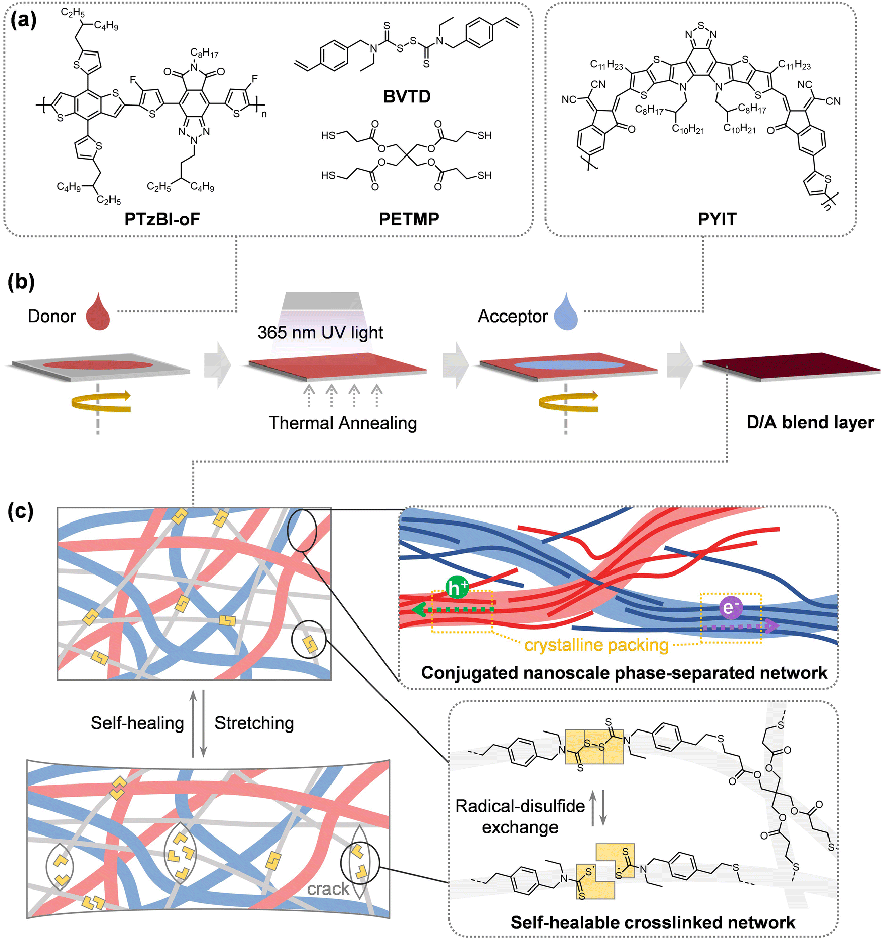 | ||
| Fig. 1 (a) Molecular structures of PTzBI-oF, BVTD, PETMP, and PYIT. (b) Fabrication of D/A blend layers with a self-healable network integrated. (c) Schematic illustration of the dual-network morphology combining a conjugated polymer phase-separated network and a S–S bond-based healable crosslinked network, where the conjugated network preserves the charge carrier transport and the self-healable network repairs the strain-induced microcracks through radical-disulfide exchanges. | ||
The success of the thiol–ene reaction was confirmed by Fourier-transform infrared (FTIR) spectroscopy and X-ray photoelectron spectroscopy (XPS). Post-crosslinking, the sulfhydryl peak (2567 cm−1) and C![[double bond, length as m-dash]](https://www.rsc.org/images/entities/char_e001.gif) C stretch (1681 cm−1) in FTIR disappeared (Fig. 2a), while XPS revealed a shift in the S 1s peak from 163.0 eV (PETMP's-SH) to 163.9 eV (C–S bonds in the network) (Fig. 2b). Similarly, the O 1s peak shifted due to altered electron density around ester groups post-reaction (Fig. 2c). Rinse tests with CF demonstrated the network's characteristics: crosslinked PTzBI-oF retained 86% of its initial absorbance, compared to 66% for the neat polymer (Fig. 2d). Time-of-flight secondary ion mass spectrometry (TOF-SIMS) depth profiling further confirmed minimal vertical compositional changes between PTzBI-oF and PYIT, preserving a mixed D/A structure critical for charge transport (Fig. 2e and f).
C stretch (1681 cm−1) in FTIR disappeared (Fig. 2a), while XPS revealed a shift in the S 1s peak from 163.0 eV (PETMP's-SH) to 163.9 eV (C–S bonds in the network) (Fig. 2b). Similarly, the O 1s peak shifted due to altered electron density around ester groups post-reaction (Fig. 2c). Rinse tests with CF demonstrated the network's characteristics: crosslinked PTzBI-oF retained 86% of its initial absorbance, compared to 66% for the neat polymer (Fig. 2d). Time-of-flight secondary ion mass spectrometry (TOF-SIMS) depth profiling further confirmed minimal vertical compositional changes between PTzBI-oF and PYIT, preserving a mixed D/A structure critical for charge transport (Fig. 2e and f).
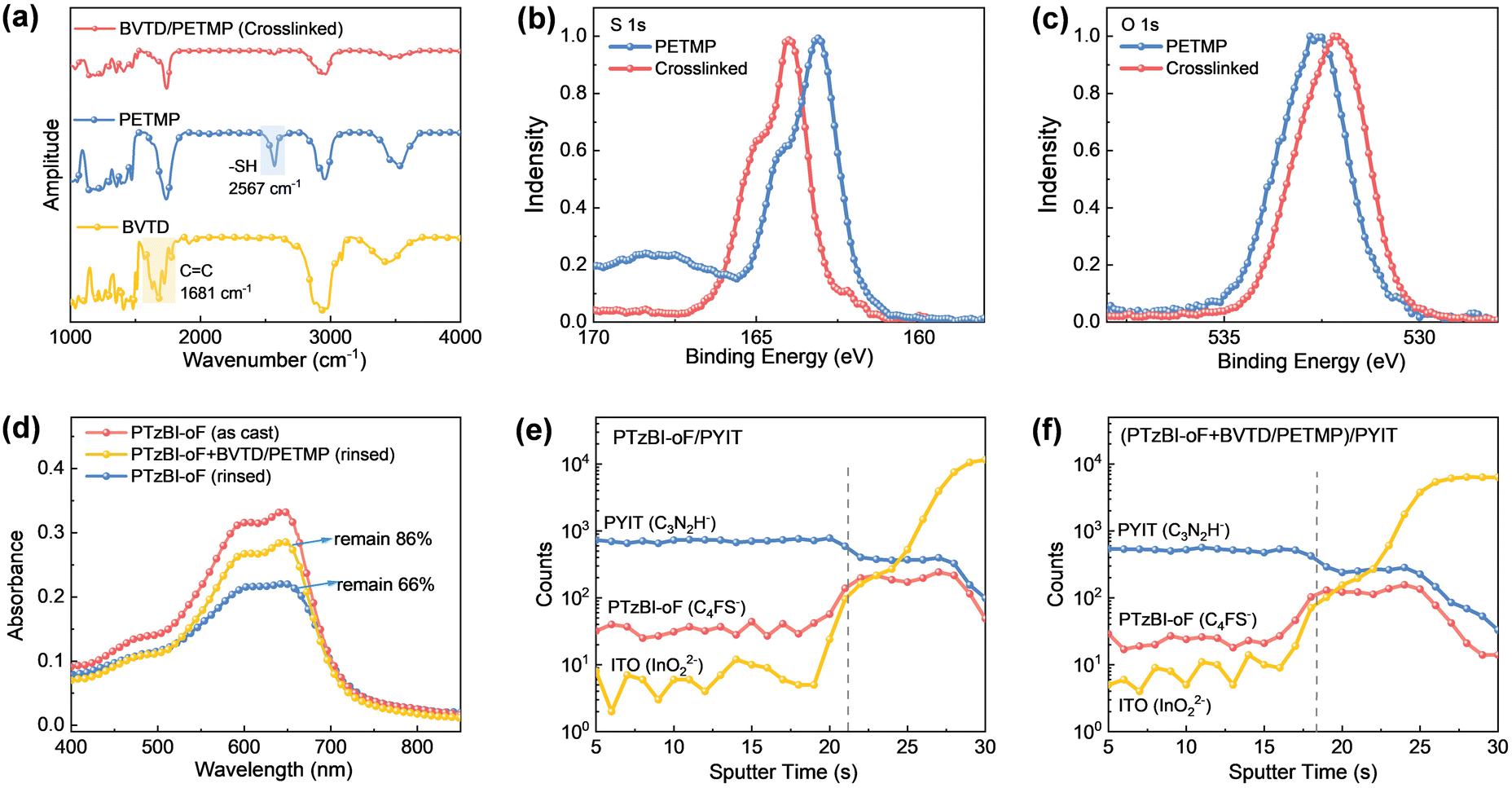 | ||
Fig. 2 (a) FTIR spectra of BVTD, PETMP, and their 2![[thin space (1/6-em)]](https://www.rsc.org/images/entities/char_2009.gif) :1 (wt:wt) blend film after the thiol–ene click reaction. (b) and (c) XPS spectra of the S 1s and O 1s core levels for PETMP and the crosslinked network. (d) Normalized UV-vis absorption spectra of as-cast PTzBI-oF films and CF-rinsed films, with and without the crosslinked network (prepared using 4 wt% BVTD relative to PTzBI-oF). TOF-SIMS depth profiles of the PTzBI-oF/PYIT active layers, (e) with and (f) without the crosslinked network, where the grey dotted lines indicate the interface between the active layers and the ITO substrate. :1 (wt:wt) blend film after the thiol–ene click reaction. (b) and (c) XPS spectra of the S 1s and O 1s core levels for PETMP and the crosslinked network. (d) Normalized UV-vis absorption spectra of as-cast PTzBI-oF films and CF-rinsed films, with and without the crosslinked network (prepared using 4 wt% BVTD relative to PTzBI-oF). TOF-SIMS depth profiles of the PTzBI-oF/PYIT active layers, (e) with and (f) without the crosslinked network, where the grey dotted lines indicate the interface between the active layers and the ITO substrate. | ||
The crosslinked network coexists with the D/A phase-separated morphology, forming a dual-network architecture (Fig. 1c). From an electronic perspective, the preserved D/A phase separation ensures efficient charge generation and transport across molecular and macroscopic scales. Mechanically, the S–S bond-based network enhances chain conformational coordination, effectively dissipating strain energy during stretching. Critically, the thiuram disulfide moieties act as dynamic units, enabling sulfur radical exchanges during tensile deformation.43–45 Under strain, S–S bonds are cleaved, and chain exchange reactions repair microcracks after strain release and room temperature storage. This self-healing process proceeds autonomously, without requiring external energy inputs such as light, heat, or pressure. Therefore, integrating this self-healable crosslinked network into conjugated polymer thin films is promising to significantly reduce optoelectronic performance losses after repeated tensile cycles.
2.2. Photovoltaic performance and device physics
To evaluate the impact of the self-healable crosslinked network on photovoltaic performance, OSCs were fabricated with the structure ITO/PEDOT:PSS/active layer/PNDIT-F3N/Ag (see the fabrication details in ESI†). Representative current density–voltage (J–V) curves are shown in Fig. 3a, with key device parameters summarized in Table 1. The control device, based on the PTzBI-oF/PYIT thin film without the network, showed a PCE of 17.55%, with a short-circuit current density (JSC) of 26.11 mA cm−2, an open-circuit voltage (VOC) of 0.891 V, and a fill factor (FF) of 75.41%. To investigate the effect of the network, varying amounts of BVTD (2%, 4%, and 8% by weight relative to PTzBI-oF) were incorporated into the PTzBI-oF solution, resulting in PTzBI-oF/PYIT blend films with increasing crosslinking density. As BVTD content increased, device PCEs gradually declined, primarily due to reductions in both JSC and FF. Despite this, the device with 4% BVTD content retained a PCE of 16.39%, with a JSC of 26.13 mA cm−2 a VOC of 0.889 V, and an FF of 74.39%. External quantum efficiency (EQE) spectra demonstrated broad and efficient photon-to-current conversion across the 300–1000 nm range (Fig. 3b), indicating that the self-healable network did not significantly compromise light absorption and charge generation. These results highlight a promising balance between mechanical durability and photovoltaic performance for the 4% BVTD-based device.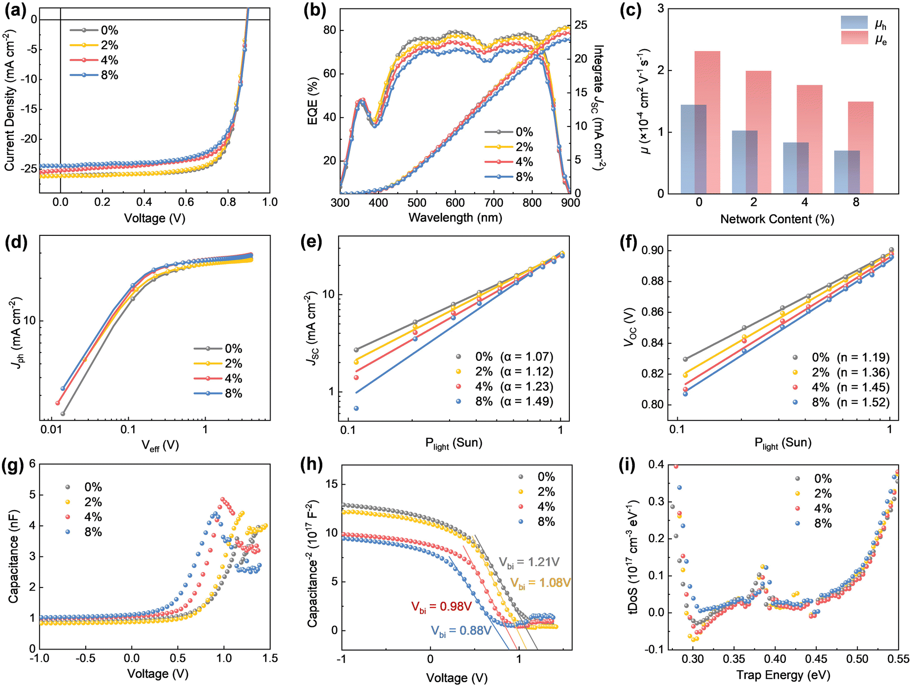 | ||
| Fig. 3 (a) J–V curves and (b) EQE spectra of OSCs fabricated with varying BVTD ratios. (c) SCLC mobilities of active layer thin films prepared with different BVTD ratios. (d) Jph–Veff curves, and Plight dependence of (e) JSC and (f) VOC for OSCs, where 1 sun corresponds to Plight = 100 mW cm−2. (g) C–V characteristics of OSCs with varying BVTD ratios. (h) 1/C2–V plots derived from the C–V curves. (i) tDoS as a function of Eω, derived from C–F characteristics. | ||
| BVTD ratio (%) | V OC (V) | J SC (mA cm−2) | J SC EQE (mA cm−2) | FFa (%) | PCEa (%) |
|---|---|---|---|---|---|
| a The parameters were averaged from 10 individual devices. | |||||
| 0 | 0.891 | 26.11 | 24.82 | 75.41 | 17.55 |
| 0.890 ± 0.004 | 26.11 ± 0.11 | 75.37 ± 0.24 | 17.53 ± 0.13 | ||
| 2 | 0.889 | 26.13 | 24.78 | 74.39 | 17.29 |
| 0.889 ± 0.003 | 26.11 ± 0.12 | 74.52 ± 0.39 | 17.29 ± 0.19 | ||
| 4 | 0.891 | 25.23 | 23.97 | 72.94 | 16.39 |
| 0.890 ± 0.003 | 25.16 ± 0.09 | 72.72 ± 0.37 | 16.27 ± 0.11 | ||
| 8 | 0.910 | 24.45 | 22.98 | 70.75 | 15.73 |
| 0.896 ± 0.005 | 24.35 ± 0.27 | 70.41 ± 0.52 | 15.36 ± 0.23 | ||
Charge mobilities were measured by the space-charge limited current (SCLC) method in charge-only devices (Fig. 3c, Fig. S2, and Table S2, ESI†). The control device showed a hole mobility (μh) of 1.44 × 10⁻⁴ cm2 V−1 s−1 and an electron mobility (μe) of 2.31 × 10⁻⁴ cm2 V−1 s−1. With the introduction of the self-healable network, μh decreased more significantly than μe, though the μe/μh ratio remained balanced (<2) for devices with up to 4% BVTD. Photocurrent density-effective voltage (Jph–Veff) curves were used to evaluate exciton dissociation and charge collection efficiencies (Fig. 3d and Table S3, ESI†).46 The control device exhibited a dissociation probability (Pdiss) of 96.12% under short-circuit condition, while devices with 2%, 4%, and 8% BVTD showed Pdiss values of 94.67%, 92.84%, and 90.11%, respectively. Charge recombination mechanisms were further analyzed using light intensity (Plight) dependence of JSC and VOC (Fig. 3e and f). The relationship JSC ∝ Pαlight yielded an α value of 1.07 for the control device, increasing to 1.12, 1.23, and 1.49 for devices with 2%, 4%, and 8% BVTD, respectively, indicating enhanced bimolecular recombination with higher BVTD content.47 Similarly, the Plight–VOC relationship, described by  , yielded an n value of 1.19 for the control device, increasing to 1.36, 1.45, and 1.52 for devices with 2%, 4%, and 8% BVTD, respectively. These trends suggest the introduction of the self-healable network leads to slight decrease in exciton dissociation efficiency and increase in recombination loss, likely contributing to the observed reductions in JSC and FF.
Mott–Schottky analysis was performed using capacitance–voltage (C–V) characteristics (Fig. 3g).48,49 The C–V relationship is described by  , where A is the device area, ε0 is the vacuum permittivity, ε is the relative permittivity of the blend film, Vbi is the built-in electric field, and NA represents the doping or impurity concentration.50,51 The 1/C2–V plots were used to derive the Vbi and NA (Fig. 3h, Fig. S3, and Table S4, ESI†). The NA values increased slightly from 1.50 × 1015 cm−3 for the control device to 1.75 × 1015 cm−3 for the 8% BVTD device, indicating a minor increase in impurity concentration due to the network. This increase likely contributed to the observed rise in trap-assisted recombination. Additionally, Vbi decreased from 1.21 V to 0.88 V as BVTD content increased, suggesting reduced carrier accumulation at the interface and a slight decline in carrier mobility. Trap state of density (tDoS) as a function of trap energy (Eω) was derived from the capacitance–frequency (C–F) characteristics (Fig. 3i and Fig. S4, ESI†).52 Gaussian fitting of tDoS revealed an increase in both average trap energy (Et) and Gaussian width (σ) with BVTD content (Fig. S5 and Table S5, ESI†). The tDoS peak shifted from 0.384 eV to 0.388 eV, indicating the formation of higher-energy and more dispersed defect levels. These traps likely arrest charge transport, contributing to the observed decline in JSC and FF. While the 4% BVTD-based device exhibits only mild performance degradation, the results highlight the importance of optimizing the network's composition to maintain efficient charge transport and minimize recombination losses.
2.3. Crystallization and dual-network morphology
The thin film structures, from crystalline packing to the self-healable network morphology, were investigated using grazing incidence wide-angle X-ray scattering (GIWAXS), atomic force microscopy-infrared spectroscopy (AFM-IR), and resonant soft X-ray scattering (RSoXS). Fig. 4a and b show the GIWAXS 2D images and sector-averaged I–q curves in the in-plane (IP) and out-of-plane (OOP) directions. The dynamic disulfide network itself exhibits an amorphous nature, as indicated by a broad scattering halo centered at 1.4 Å−1. The PTzBI-oF/PYIT thin film exhibits a preferential face-on orientation, characterized by a lamellar stacking peak at 0.30 Å−1 in the IP direction and a strong π–π stacking peak at 1.72 Å−1 in the OOP direction. These features are preserved upon integrating the self-healable network with 4% BVTD, which are advantageous to vertical charge transport in devices. Multi-peak fitting analysis of the I–q curves was performed to obtain key crystalline parameters, including d-spacing, crystalline coherence length (CCL), and crystallinity (peak area). The results show that the lamellar and π–π stacking peak areas decreased by 18% and 15%, respectively, in the presence of the self-healing network, indicating a moderate reduction in crystallinity (Fig. 4c, Fig. S6, and Table S6, ESI†). However, d-spacing and CCL remain nearly unchanged. These results suggest partial disruption of long-range order, yet the preservation of local packing motifs supports maintained charge transport pathways, as corroborated by the retained mobilities observed in SCLC measurements.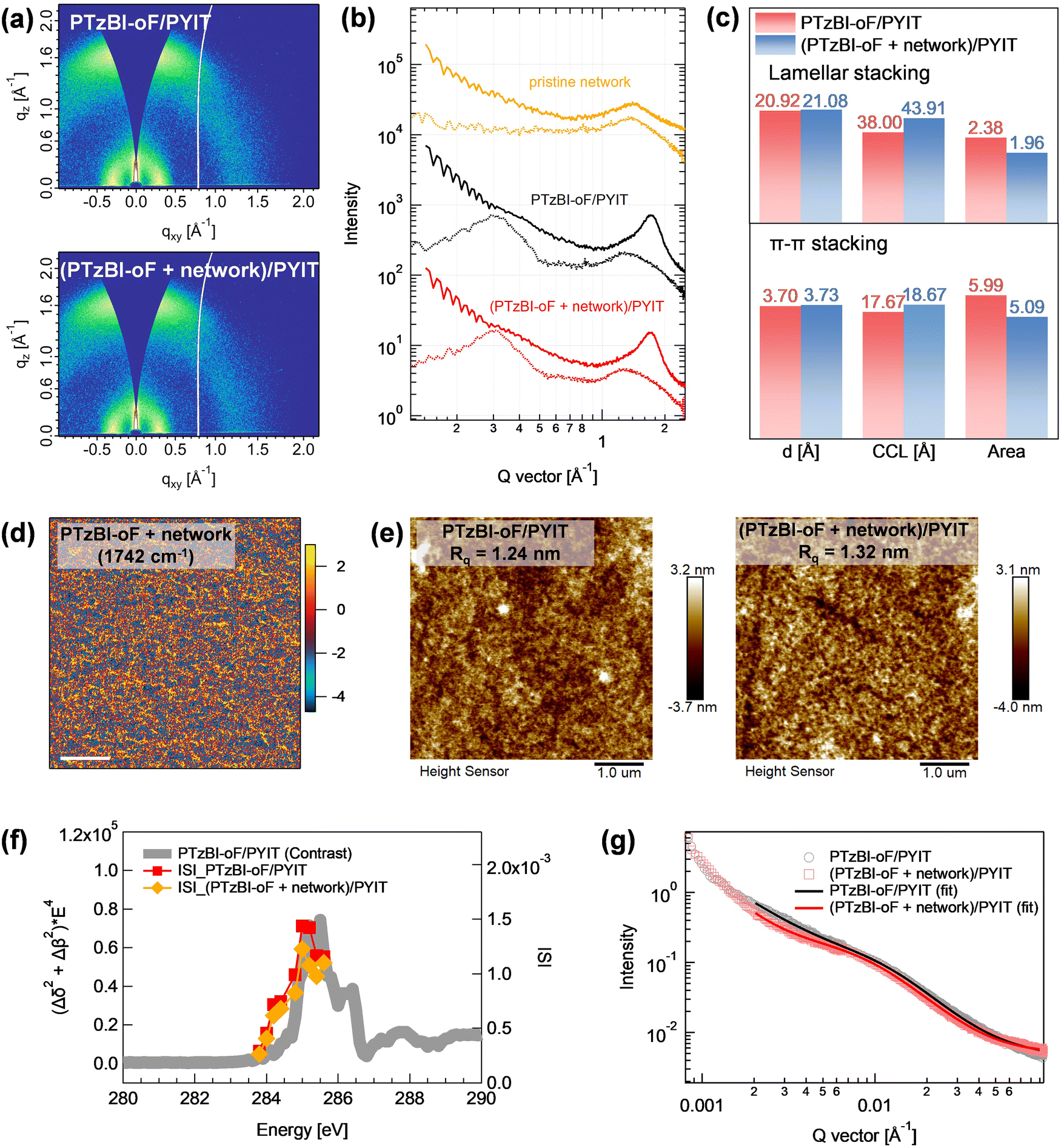 | ||
| Fig. 4 (a) GIWAXS 2D scattering images, (b) sector-averaged I–q curves in IP and OOP directions, and (c) summary of d-spacing, CCL, and peak area (crystallinity) for PTzBI-oF/PYIT thin films with and without the self-healable network. (d) AFM-IR amplitude image highlighting the network in PTzBI-oF thin film probed at 1742 cm−1. The scale bar in the image represents 0.25 μm, and the color bar indicates the IR amplitude. (e) AFM height images of PTzBI-oF/PYIT blend films. (f) RSoXS contrast function and calculated ISI values at various energies within the CC 1s → π* absorption range (283.0–286.0 eV). (g) RSoXS I–q curves at 285.0 eV of PTzBI-oF/PYIT blend films with and without the self-healable network. The solid lines are fitting results with the correlation length model. | ||
AFM-IR was used to map the phase separation in PTzBI-oF films with the network. By targeting the wavenumber at 1742 cm−1, associated with the network, AFM-IR images revealed a uniform nanoscale distribution of the network in films prepared with 4% BVTD (Fig. 4d and Fig. S7, ESI†), which was also observed for films with 8% BVTD (Fig. S8, ESI†). These results indicate high miscibility between the conjugated polymer and the self-healable network. AFM was employed to characterize the surface morphology of PTzBI-oF/PYIT blend films (Fig. 4e). Both films exhibited smooth, fibrillar structures with a root-mean-square roughness (Rq) of ∼1.3 nm. Power spectral density (PSD) analysis of the AFM images revealed a slight increase in domain sizes with network incorporation, as evidenced by higher PSD intensity at low frequencies (Fig. S9, ESI†).
RSoXS measurements at the C K-edge provided further insight into the phase-separated morphology. For PTzBI-oF with the network, no discernible scattering signals were observed, indicating a uniform mixture (Fig. S10, ESI†). The scattering intensity was dominated by the chemical contrast between PTzBI-oF and PYIT, as the calculated contrast function (Δδ2 + Δβ2) × E4 aligned with integrated scattering intensity (ISI,  ) (Fig. 4f and Fig. S11, S12, ESI†).53,54 At 285.0 eV, the energy at which scattering contrast is maximized, the ISI decreased by ∼15% upon network incorporation, suggesting reduced domain purity. This reduction likely results from the homogeneous dispersion of the self-healing network throughout the D/A blend. As shown in Fig. 4g, the RSoXS I–q curves at 285.0 eV for blend films without and with the network exhibited scattering humps at 0.015 Å−1 and 0.012 Å−1, corresponding to characteristic lengths of 41 nm and 51 nm, respectively (Fig. S13, ESI†). The characteristic lengths were also evaluated using a correlation length model:

2.4. Self-healable thin films and IS-OSCs
To evaluate the mechanical properties of neat and blend thin films, stress–strain (σ–ε) curves were measured using the free-standing method (Fig. 5a and b).18 The neat PTzBI-oF film exhibited early mechanical failure at a strain of 8.9% (Table S8, ESI†). Incorporating the self-healable network by varying the BVTD ratio (2%, 4%, and 8%) significantly improved mechanical resilience, with COS values increasing to 15.6%, 17.6%, and 22.4%, respectively. For PTzBI-oF/PYIT blend films, similar trends were observed, though COS values were lower due to the brittle nature of PYIT. Specifically, COS values for blend films with 0%, 2%, 4%, and 8% BVTD were 7.1%, 10.9%, 15.6%, and 18.6%, respectively. These results demonstrate that the self-healable network shifts the fracture mode to a more ductile behavior. Molecular dynamics (MD) simulations were conducted to investigate the effect of the healable network on molecular mobility. Model polymer chains of PTzBI-oF and PYIT were embedded in an amorphous cell with varying concentrations of dynamic disulfide networks and subjected to stretching simulations using the Forcite module under applied stresses up to 1.5 GPa (Fig. S14, ESI†). The center-of-mass displacement of PYIT progressively decreased with increasing network content: from 33 Å in the pristine blend, to 16.6 Å with 4%-BVTD network, and 11.3 Å with 8%-BVTD network. These results demonstrate that higher crosslink density restricts molecular mobility, thereby leading to improved mechanical resilience. | ||
| Fig. 5 Stress–strain curves of (a) neat PTzBI-oF films and (b) PTzBI-oF/PYIT blend films incorporating a self-healable network with varying BVTD ratios (2%, 4%, and 8%). Optical microscopy images of the self-healing process for PTzBI-oF/PYIT films prepared with (c) 4% BVTD, (d) 8% BVTD and (e) 80% BVTD, showing crack closure over time. (f) Device architecture used for IS-OSCs. (g) Normalized PCE as a function of strain for IS-OSC devices fabricated with 8% BVTD. Inset shows the digital images of the devices under different deformation processes. | ||
Next, we studied the self-healable capabilities of the PTzBI-oF/PYIT blend films with the network through mechanical recovery tests. Films were stretched to induce microcracks and then stored at room temperature for 30 minutes to allow for healing (Fig. 5c–e). Optical microscopy imaging revealed that the cracks progressively healed over time for both (PTzBI-oF + network)/PYIT blend films prepared with 4% and 8% BVTD, demonstrating efficient self-healing behavior. Such effect was more pronounced in films with higher network content (prepared with 80% BVTD), where larger cracks showed distinct closure. This self-healing ability is crucial for enabling IS-OSC devices to withstand repeated high-strain cycles.
To further investigate the recovery of photovoltaic performance, IS-OSC devices with the structure TPU/PEDOT:PSS (M-PH1000)/PEDOT:PSS (4083)/active layer/PNDIT-F3N/EGaIn@Ag were fabricated (Fig. 5f; see fabrication process in ESI†). The M-PH1000 and EGaIn@Ag were used as the stretchable electrodes.29 For rigid devices, 4% BVTD was identified as the optimal ratio to balance crosslink density with photovoltaic performance. In contrast, IS-OSC devices employed a higher BVTD ratio (8%) to prepare the healable network for enhancing mechanical stretchability and self-healing efficiency, while still maintaining a baseline PCE approaching 16%. The devices were stretched to 40% strain (1st stretching) to induce cracks, then returned to 0% strain and stored for self-healing before applying strain again (2nd stretching). The J–V curves of the device under different strains are shown in Fig. S15 (ESI†), and device parameters are summarized in Table S9 (ESI†). As shown in Fig. 5g, the device initially had a PCE of 9.64% (VOC = 0.881 V, JSC = 23.09 mA cm−2, FF = 46.91%). As increasing strain applied, degradation in PCE was seen, which dropped to 7.72% (80% relative to the initial value) at 30% strain. This degradation is likely due to strain-induced crystalline peeling in the lamellar stacking, evidenced by the decreased peak area and packing number from GIWAXS performed with X-ray direction perpendicular to the stretch direction (Fig. S16–S19 and Table S10, ESI†). To assess the impact of network incorporation on charge transport under strain, photo-CELIV measurements were performed on IS-OSC devices upon stretching (Fig. S20 and Table S11, ESI†). For the control PTzBI-oF/PYIT device, the mobility sharply declined from 7.51 × 10⁻⁵ cm2 V−1 s−1 to 0.31 × 10⁻⁵ cm2 V−1 s−1 as strain increased to 20%. In contrast, the device with 8%-BVTD network retained a significantly higher mobility of 3.99 × 10⁻⁵ cm2 V−1 s−1 at 20% strain (from an initial 6.92 × 10⁻⁵ cm2 V−1 s−1). Such results suggest that, despite some crystallite disruption, the dynamic network plays a crucial role in sustaining charge transport pathways during deformation, contributing to enhanced mechanical robustness and the more gradual decline in JSC observed in the network-integrated devices.
After recovery from 40% strain to 0%, the PCE rebounded to 8.25%. With the self-healable network, the device showed a recovery to 9.53% (99% of the initial PCE) after storage for 30 minutes. During the second stretching, the PCE followed a similar decrease trend as the first stretch. In contrast, no recovery was observed for the control PTzBI-oF/PYIT device, which exhibited a >50% decrease in PCE during the second stretch (Fig. S21 and Table S12, ESI†). In situ UV-vis-NIR absorption spectroscopy on PTzBI-oF/PYIT thin film was measured to track the molecular packing changes under 20% strain during stretching-recovery cycles (Fig. S22, ESI†). We observed a red-shift of the PYIT absorption from 811 to 815 nm upon stretching, suggesting an increase in effective conjugated length of PYIT packing. Following recovery and 30 minutes of healing, both the absorbance and peak position returned nearly to their original state, indicating spontaneous reformation of the network structure. Similar trend was seen during the second cycle. This optical recovery aligns with the device's restored PCE after strain release, confirming that the dynamic disulfide bond network not only accommodates mechanical deformation but also drives autonomous morphological reorganization.
To evaluate long-term operational reliability, the IS-OSCs were subjected to 200 cycles of 20% tensile strain using a programmable tensile stage with an initial clamp-to-clamp distance of ∼3 mm and a motor speed of 0.08 mm min−1. After every 50 cycles, the devices were allowed to rest for 5 min before testing to enable self-healing process. The devices retained ∼80% of their initial PCE after 100 cycles and remained operational after 200 cycles in a nitrogen-filled glove box (25 °C, O2 < 5 ppm, H2O <0.01 ppm), indicating good mechanical durability under repeated deformation (Fig. S23 and Table S13, ESI†). To evaluate environmental robustness, we tested the IS-OSCs under ambient conditions (25 °C, atmospheric oxygen, ∼40% RH), subjecting them to the same 200-cycle strain protocol. Compared to the inert glovebox environment, devices exhibited faster performance degradation in air (Fig. S24 and Table S14, ESI†), likely due to moisture-induced deterioration of the PEDOT:PSS based electrode and interfacial layer. Despite this, the devices still retained over 50% of their initial PCE after 200 strain cycles, indicating partial resilience and operational viability under practical environmental conditions. Thus, the incorporated dynamic network facilitated the self-healing of microcracks or interface disruptions within the active layer during each rest period. This recovery behavior is supported by the fact that the non-healable control device showed significant and fast degradation after only two stretch cycles (Fig. S21, ESI†), highlighting the critical role of the self-healable network in enhancing long-term mechanical stability and sustaining performance under repeated deformation.
To examine scalability, we investigated the film uniformity of 8% BVTD-based active layers spin-coated on a larger substrate (1.7 × 1.7 cm2). The pristine PTzBI-oF/PYIT thin film showed slight edge-to-center variation in thickness (Fig. S25, ESI†). The presence of the healable network did not alter the thickness uniformity and surface flatness across the substrate, indicating good compatibility with large-area fabrication. Furthermore, we fabricated large-area devices (active area = 1 cm2) using this process, showing functional device operation with PCE of 4.88% (VOC = 0.881 V, JSC = 18.36 mA cm−2, FF = 30.14%) (Fig. S26, ESI†). Although efficiency requires further optimization due to current process limitations, these results highlight the promise of our self-healable system for scalable, large-area stretchable photovoltaic applications.
Therefore, our results demonstrate that the self-healable network enables IS-OSCs to recover optoelectronic performance at room temperature, even after high-strain cycles. This proof-of-concept highlights the potential of self-healable IS-OSCs for applications requiring both mechanical durability and photovoltaic efficiency. To further illustrate practical relevance, the IS-OSC device was mounted on a human finger, conforming seamlessly to the curved surface without delamination. The device also withstood stretching, bending, and twisting deformations, maintaining its structural integrity and returning to its original shape without visible damage (Fig. S27, ESI†).
3. Conclusion
In this work, we developed a self-healable crosslinked network integrated into organic photovoltaic blend films. This network exhibits high miscibility with conjugated polymers, preserving both the crystalline packing of the polymer and the nanoscale phase-separated D/A morphology, thereby creating a dual-network architecture. The incorporation of small amounts of the self-healable network does not significantly compromise the electrical properties of the blend films. Instead, it enhances mechanical resilience through restricted molecular mobility. This results in a two-fold increase in the COS of the thin films. Crucially, the dynamic nature of the disulfide bonds facilitates sulfur radical exchanges, enabling autonomous self-healing of microcracks at room temperature. Leveraging this mechanism, we demonstrated a proof-of-concept for self-healable IS-OSCs that retain their efficiency through multiple loading-unloading cycles. These findings not only advance the development of efficient and mechanically durable IS-OSCs but also open new opportunities for other flexible electronic devices requiring both high performance and long-term reliability under mechanical stress.Data availability
The data supporting this article have been included as part of the ESI.†Conflicts of interest
The authors declare no conflict of interest.Acknowledgements
This work was financially supported by National Key Research & Development Program of China (2023YFB3609000), Guangdong Basic and Applied Basic Research Foundation (2023B1515040026), and Fundamental Research Funds for the Central Universities (2024ZYGXZR076). RSoXS was performed at beamline 11.0.1.2 at the Advanced Light Source, a U. S. DOE Office of Science User Facility under contract no. DE-AC02-05CH11231.References
- D. J. Lipomi, B. C. K. Tee, M. Vosgueritchian and Z. Bao, Adv. Mater., 2011, 23, 1771 CrossRef CAS PubMed.
- J. S. Park, G.-U. Kim, S. Lee, J.-W. Lee, S. Li, J.-Y. Lee and B. J. Kim, Adv. Mater., 2022, 34, 2201623 CrossRef CAS PubMed.
- J. Qin, L. Lan, S. Chen, F. Huang, H. Shi, W. Chen, H. Xia, K. Sun and C. Yang, Adv. Funct. Mater., 2020, 30, 2002529 CrossRef CAS.
- J.-W. Lee, E. S. Oh, S. Lee, T. N.-L. Phan, T.-S. Kim, J.-Y. Lee, J. R. Reynolds and B. J. Kim, Joule, 2025, 9, 101792 CrossRef CAS.
- D. Han, K. Zhou, X. Li, P. Lv, J. Wu, H. Ke, W. Zhao and L. Ye, Adv. Funct. Mater., 2024, 34, 2407392 CrossRef CAS.
- J. Wang, Y. Ochiai, N. Wu, K. Adachi, D. Inoue, D. Hashizume, D. Kong, N. Matsuhisa, T. Yokota, Q. Wu, W. Ma, L. Sun, S. Xiong, B. Du, W. Wang, C.-J. Shih, K. Tajima, T. Aida, K. Fukuda and T. Someya, Nat. Commun., 2024, 15, 4902 CrossRef CAS.
- J. Noh, G.-U. Kim, S. Han, S. J. Oh, Y. Jeon, D. Jeong, S. W. Kim, T.-S. Kim, B. J. Kim and J.-Y. Lee, ACS Energy Lett., 2021, 6, 2512 CrossRef CAS.
- L. Zhu, M. Zhang, Z. Zhou, W. Zhong, T. Hao, S. Xu, R. Zeng, J. Zhuang, X. Xue, H. Jing, Y. Zhang and F. Liu, Nat. Rev. Electr. Eng., 2024, 1, 581 CrossRef.
- L. Zhu, M. Zhang, G. Zhou, Z. Wang, W. Zhong, J. Zhuang, Z. Zhou, X. Gao, L. Kan, B. Hao, F. Han, R. Zeng, X. Xue, S. Xu, H. Jing, B. Xiao, H. Zhu, Y. Zhang and F. Liu, Joule, 2024, 8, 3153 CrossRef CAS.
- W. Zhong, M. Zhang, L. Zhu, Y. Zhang and F. Liu, Trends Chem., 2022, 4, 699 CrossRef CAS.
- H. Chen, Z. Zhang, P. Wang, Y. Zhang, K. Ma, Y. Lin, T. Duan, T. He, Z. Ma, G. Long, C. Li, B. Kan, Z. Yao, X. Wan and Y. Chen, Energy Environ. Sci., 2023, 16, 1773 RSC.
- X. Cao, J. Guo, Z. Li, X. Bi, H. Liang, Z. Xiao, Y. Guo, X. Jia, Z. Xu, K. Ma, Z. Yao, B. Kan, X. Wan, C. Li and Y. Chen, ACS Energy Lett., 2023, 8, 3494 CrossRef CAS.
- J. Song, C. Li, H. Ma, B. Han, Q. Wang, X. Wang, D. Wei, L. Bu, R. Yang, H. Yan and Y. Sun, Adv. Mater., 2024, 36, 2406922 CrossRef CAS PubMed.
- Z. Jia, S. Qin, L. Meng, Q. Ma, I. Angunawela, J. Zhang, X. Li, Y. He, W. Lai, N. Li, H. Ade, C. J. Brabec and Y. Li, Nat. Commun., 2021, 12, 178 Search PubMed.
- S. P. O. Danielsen, C. R. Bridges and R. A. Segalman, Macromolecules, 2022, 55, 437 CrossRef CAS.
- S. E. Root, S. Savagatrup, A. D. Printz, D. Rodriquez and D. J. Lipomi, Chem. Rev., 2017, 117, 6467 CrossRef CAS PubMed.
- S. Zhang, A. Alesadi, G. T. Mason, K.-L. Chen, G. Freychet, L. Galuska, Y.-H. Cheng, P. B. J. S. Onge, M. U. Ocheje, G. Ma, Z. Qian, S. Dhakal, Z. Ahmad, C. Wang, Y.-C. Chiu, S. Rondeau-Gagné, W. Xia and X. Gu, Adv. Funct. Mater., 2021, 31, 2100161 CrossRef CAS.
- X. Luo, G. Freychet, Z. Gan, K. An, H. Du, C. Wang, N. Li, W. Zhong and L. Ying, Macromolecules, 2023, 56, 8928 CrossRef CAS.
- J.-W. Lee, S. Seo, S.-W. Lee, G.-U. Kim, S. Han, T. N.-L. Phan, S. Lee, S. Li, T.-S. Kim, J.-Y. Lee and B. J. Kim, Adv. Mater., 2022, 34, 2207544 Search PubMed.
- J.-W. Lee, H.-G. Lee, E. S. Oh, S.-W. Lee, T. N.-L. Phan, S. Li, T.-S. Kim and B. J. Kim, Joule, 2024, 8, 204 CrossRef CAS.
- Q. Wan, S. Seo, S.-W. Lee, J. Lee, H. Jeon, T.-S. Kim, B. J. Kim and B. C. Thompson, J. Am. Chem. Soc., 2023, 145, 11914 Search PubMed.
- Y. Ding, W. A. Memon, D. Zhang, Y. Zhu, S. Xiong, Z. Wang, J. Liu, H. Li, H. Lai, M. Shao and F. He, Angew. Chem., Int. Ed., 2024, 63, e202403139 CrossRef CAS PubMed.
- M. Li, K. Xian, W. Zhao, D. Sheng, C. Liu, X. Li, W. Li and L. Ye, Chem. Eng. J., 2023, 476, 146723 CrossRef CAS.
- X. Zheng, X. Wu, Q. Wu, Y. Han, G. Ding, Y. Wang, Y. Kong, T. Chen, M. Wang, Y. Zhang, J. Xue, W. Fu, Q. Luo, C. Ma, W. Ma, L. Zuo, M. Shi and H. Chen, Adv. Mater., 2024, 36, 2307280 CrossRef CAS PubMed.
- X. Wu, X. Zheng, T. Chen, S. Zhang, Y. Zhou, M. Wang, T. Chen, Y. Wang, Z. Bi, W. Fu, M. Du, W. Ma, L. Zuo and H. Chen, Adv. Mater., 2024, 36, 2406879 CrossRef CAS.
- Z. Wang, M. Xu, Z. Li, Y. Gao, L. Yang, D. Zhang and M. Shao, Adv. Funct. Mater., 2021, 31, 2103534 CrossRef CAS.
- J. Han, F. Bao, D. Huang, X. Wang, C. Yang, R. Yang, X. Jian, J. Wang, X. Bao and J. Chu, Adv. Funct. Mater., 2020, 30, 2003654 CrossRef CAS.
- J. Zhang, Q. Chen, M. Li, G. Zhang, Z. Zhang, X. Deng, J. Xue, C. Zhao, C. Xiao, W. Ma and W. Li, Adv. Mater., 2024, 36, 2312805 CrossRef CAS PubMed.
- W. Yang, X. Luo, M. Li, C. Shi, Z. Wang, Z. Yang, J. Wu, X. Zhang, W. Huang, D. Ma, C. Wang, W. Zhong and L. Ying, Adv. Energy Mater., 2025, 15, 2403259 CrossRef CAS.
- X. Li, H. Ke, S. Li, M. Gao, S. Li, J. Yu, H. Xie, K. Zhou, K. Zhang and L. Ye, Adv. Funct. Mater., 2024, 34, 2400702 CrossRef CAS.
- Z. Wang, D. Zhang, M. Xu, J. Liu, J. He, L. Yang, Z. Li, Y. Gao and M. Shao, Small, 2022, 18, 220158 Search PubMed.
- Z. Wang, D. Zhang, L. Yang, M. Xu, J. Liu, Z. Wang, Y. Gao, L.-Y. Zhang, L. Niu and M. Shao, ACS Mater. Lett., 2024, 6, 4710 CrossRef CAS.
- J. Zuo, D. Han, H. Yao, V. Kuvondikov and L. Ye, Energy Environ. Sci., 2025 10.1039/d5ee01504a.
- Z. Wang, D. Zhang, L. Yang, O. Allam, Y. Gao, Y. Su, M. Xu, S. Mo, Q. Wu, Z. Wang, J. Liu, J. He, R. Li, X. Jia, Z. Li, L. Yang, M. D. Weber, Y. Yu, X. Zhang, T. J. Marks, N. Stingelin, J. Kacher, S. S. Jang, A. Facchetti and M. Shao, Science, 2025, 387, 381–387 CrossRef CAS.
- J.-W. Lee, E. S. Oh, S. Lee, T. N.-L. Phan, T.-S. Kim, J.-Y. Lee, J. R. Reynolds and B. J. Kim, Joule, 2025, 9, 101792 CrossRef CAS.
- J.-W. Lee, T. H.-Q. Nguyen, W. J. Kang, S. Seo, S. Lee, S. Lee, J. Choi, J. Park, J.-Y. Lee, T.-S. Kim and B. J. Kim, Energy Environ. Sci., 2025, 18, 3325–3340 RSC.
- W. Tang, Z. Ding, Y. Su, Q. Weng, Y. Zhang, R. Li, W. Huang, Z. Wang, Y. Wu, Y. Han, K. Zhao, Z. Yang, X. Wang and S. Liu, Adv. Funct. Mater., 2024, 34, 2312289 CrossRef CAS.
- K. Xian, K. Zhang, T. Zhang, K. Zhou, Z. Zhang, J. Hou, H. Zhang, Y. Geng and L. Ye, Energy Environ. Sci., 2025, 18, 2570–2583 RSC.
- K. Zhou, D. Han, K. Xian, S. Li, M. Gao, K. Zhang, B. Zhao, X. Li, Y. Chen, Y. Geng and L. Ye, Energy Environ. Sci., 2024, 17, 5950–5961 RSC.
- K. Zhou, K. Xian, R. Ma, J. Liu, M. Gao, S. Li, T. Liu, Y. Chen, Y. Geng and L. Ye, Energy Environ. Sci., 2023, 16, 5052–5064 RSC.
- S. Lee, S. Oh, S. Han, D. Lee, J. Lee, Y. Kim, H.-Y. Jeong, J.-W. Lee, M.-H. Lee, W. B. Ying, S. Jeong, S. Lee, J. Kim, Y. H. Kim, B. J. Kim, E.-C. Jeon, T.-S. Kim, S. Cho and J.-Y. Lee, Energy Environ. Sci., 2024, 17, 8915–8925 Search PubMed.
- X. Yang, L. Cheng, Z. Zhang, J. Zhao, R. Bai, Z. Guo, W. Yu and X. Yan, Nat. Commun., 2022, 13, 6654 Search PubMed.
- Y. Amamoto, H. Otsuka, A. Takahara and K. Matyjaszewski, Adv. Mater., 2012, 24, 3975 CrossRef CAS.
- S. Wang and M. W. Urban, Nat. Rev. Mater., 2020, 5, 562 CrossRef CAS.
- N. J. Bongiardina, S. M. Soars, M. Podgorski and C. N. Bowman, Polym. Chem., 2022, 13, 3991 Search PubMed.
- W. Zhong, J. Cui, B. Fan, L. Ying, Y. Wang, X. Wang, G. Zhang, X.-F. Jiang, F. Huang and Y. Cao, Chem. Mater., 2017, 29, 8177 Search PubMed.
- R. A. Street, K. W. Song, J. E. Northrup and S. Cowan, Phys. Rev. B: Condens. Matter Mater. Phys., 2011, 83, 165207 Search PubMed.
- W. Yao, Z. Wu, E. Huang, L. Huang, A. E. London, Z. Liu, J. D. Azoulay and T. N. Ng, ACS Appl. Electron. Mater., 2019, 1, 660–666 Search PubMed.
- T. Kirchartz, W. Gong, S. A. Hawks, T. Agostinelli, R. C. I. MacKenzie, Y. Yang and J. Nelson, J. Phys. Chem. C, 2012, 116, 7672–7680 Search PubMed.
- B. Xiao, M. Zhang, J. Yan, G. Luo, K. Gao, J. Liu, Q. You, H.-B. Wang, C. Gao, B. Zhao, X. Zhao, H. Wu and F. Liu, Nano Energy, 2017, 39, 478–488 CrossRef CAS.
- X. Zhang, J. Zhang, D. Phuyal, J. Du, L. Tian, V. A. Oberg, M. B. Johansson, U. B. Cappel, O. Karis, J. Liu, H. Rensmo, G. Boschloo and E. M. Johansson, Adv. Energy Mater., 2018, 8, 1702049 CrossRef.
- H. Aqoma, M. Mubarok, W. Hadmojo, E. Lee, T. Kim, T. Ahn, S. Oh and S. Jang, Adv. Mater., 2017, 29, 1605756 Search PubMed.
- W. Zhong, M. Zhang, G. Freychet, G. M. Su, L. Ying, F. Huang, Y. Cao, Y. Zhang, C. Wang and F. Liu, Adv. Mater., 2022, 34, 2107316 Search PubMed.
- B. A. Collins, J. E. Cochran, H. Yan, E. Gann, C. Hub, R. Fink, C. Wang, T. Schuettfort, C. R. McNeill, M. L. Chabinyc and H. Ade, Nat. Mater., 2012, 11, 536 Search PubMed.
- Z. Li, J. Xie, W. Wang, Z. Yang, L. Kan, M. Zhang, Z. Wang, W. Yang, F. Peng, W. Zhong and L. Ying, Energy Environ. Sci., 2025, 18, 3026–3035 Search PubMed.
- H. Zhuo, X. Li, J. Zhang, C. Zhu, H. He, K. Ding, J. Li, L. Meng, H. Ade and Y. Li, Nat. Commun., 2023, 14, 7996 Search PubMed.
Footnote |
| † Electronic supplementary information (ESI) available. See DOI: https://doi.org/10.1039/d5ee01082a |
| This journal is © The Royal Society of Chemistry 2025 |