
 Open Access Article
 This Open Access Article is licensed under a Creative Commons Attribution-Non Commercial 3.0 Unported Licence
Spontaneous passivation of selective Zn(101) plating via dangling bond saturation and electrostatic interaction regulation for high-utilization, fast-kinetics zinc anodes†
Yuxuan
Zhang
a,
Minyoung
Kim
a,
Dong Hun
Lee
a,
Fei
Qin
a,
Han-Wook
Song
b,
Chung Soo
Kim
c,
Jeongmin
Park
cd,
Chohee
Kim
ce,
Fang
Lian
 f and
Sunghwan
Lee
*a
f and
Sunghwan
Lee
*a
aSchool of Engineering Technology, Purdue University, West Lafayette, IN 47907, USA. E-mail: sunghlee@purdue.edu
bConvergence Research Center for Meta-Touch, Korea Research Institute of Standards and Science (KRISS), Daejeon, Republic of Korea
cAnalysis and Standards Center, Korea Institute of Ceramic and Technology, Jinju, 52851, Republic of Korea
dGraduate School of Semiconductor Materials and Devices Engineering, Ulsan National Institute of Science and Technology, Ulsan, 44919, Republic of Korea
eDepartment of Materials Science and Engineering, Pusan National University, Pusan, 43241, Republic of Korea
fSchool of Materials Science and Engineering, University of Science and Technology Beijing, Beijing, 100083, P. R. China
First published on 14th March 2025
Abstract
Although Zn(101) exhibits faster Zn2+ plating/stripping kinetics and stronger bonding with Zn2+ compared to Zn(002), the application of Zn(101) in Zn batteries has been limited due to its higher reactivity with water. However, a novel approach utilizing spontaneous self-passivation of plated Zn(101) offers the potential to harness its favorable kinetics and stronger Zn–Zn bonding for battery applications. Here, we present a high-utilization and fast-kinetics Zn anode by promoting selective (101) facet growth and achieving spontaneous passivation of the underlying Zn plating. A non-stoichiometric Sn–O system is selected as the modification material because of its ability to engineer crystal structures (amorphous, rutile, and layered) and manipulate electrical polarity (n-type vs. p-type). The optimized p-type SnO1.17 saturates dangling bonds of Zn(101), benefiting the preferential growth of well-aligned Zn(101) planes. Besides, the Zn2+ plating location is altered underlying the interphase due to synergetic effects of lower Zn2+ migration barriers of the layered structure and electron-blocking properties of SnO1.17. Consequently, a high Zn utilization ratio of over 91.5% is achieved in 800 hours, with an impressively low overpotential of 43 mV. Furthermore, an anode-free system combining a ZnMn2O4 cathode and a SnO1.17@Cu anode retained 81.6% capacity after 200 cycles.
Broader contextInducing (002)-oriented Zn2+ plating has been widely explored as an effective strategy for achieving reversible Zn2+ plating/stripping, largely due to its resistance to water-triggered parasitic reactions. However, the weak bonding between Zn2+ and the Zn(002) plane often leads to lattice distortion at high Zn plating amounts. Furthermore, the slower mass transfer at Zn(002) can result in sluggish Zn2+ plating/stripping kinetics. In contrast, the Zn(101) plane offers faster mass transfer kinetics and stronger Zn2+ bonding; yet, its high reactivity towards water has limited its application. To leverage the advantages of Zn(101) while maintaining electrochemical stability, we constructed a SnO1.17 interphase on the anode. This interphase guided Zn2+ plating beneath its structure with a regulated (101) orientation, effectively isolating the (101)-oriented Zn from water molecules and eliminating water-triggered parasitic reactions. The SnO1.17 interphase further facilitates rapid Zn2+ transfer and provides low polarization, reducing voltage hysteresis during cycling. Additionally, the stronger interaction between Zn2+ and the Zn (101) plane prevents lattice distortion even at high Zn plating amounts, resulting in well-aligned Zn(101) planes. This study underscores the potential of oriented Zn2+ plating along the (101) facet to achieve a high Zn utilization ratio and superior Zn anode kinetics. |
Introduction
Zn ion batteries (ZIBs) with mild aqueous electrolytes (i.e., ZnSO4) have been considered grid-level energy storage solutions due to their high theoretical capacity (820 mA h![[thin space (1/6-em)]](https://www.rsc.org/images/entities/char_2009.gif) g−1), resource abundance, and eco-friendliness.1–3
g−1), resource abundance, and eco-friendliness.1–3
However, the uncontrollable Zn dendrite growth, hydrogen evolution reaction (HER), and corrosion severely limit the reversibility and lifespan of ZIBs.4,5 These issues are more detrimental to practical ZIBs, which require a negative/positive (N/P) capacity ratio lower than 1.08 (referenced to the commercialized lithium-ion batteries, LIBs).6,7 A Zn utilization ratio (ZUR) higher than 80% is the prerequisite to realize this low N/P ratio.8 The low ZUR and poor reversibility significantly undermine the advantages of ZIBs compared to alternative technologies such as lithium-ion and sodium-ion batteries. The characteristics of plated Zn, which are normally dominated by the crystallographic (002), (100), and (101) facets of hexagonal close-packed Zn, are highly correlated to the Zn stripping/plating behaviors and concomitant side reactions.9–11 According to the Gibbs–Curie–Wulff theorem, the (002) facet of Zn metal has a lower reactivity towards water and a slower growth rate due to the lower surface energy compared to that of the (001) and (101) facets.12,13 Therefore, attention has been focused on inducing the crystalline orientation of plated Zn along the (002) plane, which may reduce dendritic growth, HER, and corrosion.14–16 Archer et al. employed graphene as the anode to induce the (002) oriented growth of Zn2+ plating, leading to enhanced Zn2+ stripping/plating reversibility.17 Subsequently, a series of materials such as metallic sulfides, MXenes, and metal–organic frameworks followed the work to modulate the orientation of plated Zn along the (002) facet, which suppressed the formation of dendrites to some extent.18–20 In addition to the anode modifications, separator alterations (e.g., by sulfonic cellulose coating) and the adoption of electrolyte additives (e.g., anionic surfactants) have also been demonstrated to regulate Zn2+ plating along the (002) facet.21,22
Despite the effect being somewhat demonstrated, the slower growth rate of Zn(002) compared to Zn(100) and (101) results in a larger polarization during Zn stripping/plating, which negatively impacts battery performance.23–25 In addition, as research into Zn(002) has progressed, it has been verified that the plated Zn orientation easily deviates from the intended (002) facet, resulting in significant lattice distortion and irreversible Zn2+ plating/stripping, due to the weak bonding between the (002) facet and the plated Zn atoms, further compromising structural integrity and efficiency.9,26 It is urgent to establish an alternative solution to achieve a high ZUR and kinetically favorable Zn2+ plating/stripping process.
Although vulnerable to HER and corrosion reactions, Zn(101) has garnered increasing attention from researchers due to its faster growth rates compared to other major facets and stronger Zn–Zn bonding to maintain the desired facet, which shows feasibility to address issues associated with Zn(002). For example, Liu et al. demonstrated that the epitaxial growth of the Zn(101) facet can be achieved by constructing a highly oriented Zn(101) substrate, resulting in exceptional Zn2+ plating kinetics.24 Electrolyte additives such as theophylline and dextrin have also been shown to promote the preferential growth of the Zn(101) facet, where the additives are selectively adsorbed onto Zn(002) and Zn(100) facets, directing Zn2+ to migrate to and deposit along the (101) facet.25,27 However, in these studies, the plated Zn(101) is directly exposed to water molecules, leading to inevitable HERs, corrosion reactions, and dendrite growth—issues that will be drastically exaggerated with increased Zn2+ plating/stripping amounts. Consequently, the ZUR is critically limited to below 40%, compromising reversibility and energy density.24,25,27–29
The primary goal of this study is to harness the favorable kinetics and stronger Zn–Zn bonding strength of Zn(101) towards sustainable Zn anode applications, particularly featuring a high ZUR (>80%). To this end, the following hypotheses were established: (a) selective Zn orientation (in this study (101)) may be achieved by saturating the Zn dangling bonds of the selected (101) facet of Zn. (b) The highly reactive Zn(101) can be spontaneously passivated by an artificial interphase that can shield Zn2+ from electrons and rapidly transport Zn2+ throughout the interphase. (c) The formation of Zn dendrites can be restricted by an artificial interphase with a high Young's modulus (>100 GPa).
These hypotheses were formulated from the well-known facts that (1) the existence of dangling bonds is directly associated with surface energy, which raises the nucleation energy barrier and consequently limits the growth of crystalline phases;12,30 (2) the Zn2+ plating location is governed by Zn2+ diffusion and electron reduction. The rapid diffusion of Zn2+, coupled with limited electron availability within the material, may prevent the reduction of Zn2+ upon coming into contact with the interphase. This allows Zn2+ to migrate through the interphase until the ions reach its end, where Zn begins plating beneath the interphase upon encountering an electron source (i.e., Zn electrode), immediately being isolated from water/electrolyte;31,32 and (3) Zn dendrites, whose Young's modulus is as high as ∼100GPa, have been reported to penetrate the artificial interphase of low mechanical strength and cause an internal short circuit.17,33 Therefore, the mechanical properties of the implemented artificial interphases need to be greater than those of Zn dendrites.
To identify optimal materials for constructing an artificial interphase for the Zn anode, the candidate materials were divided into five main categories: carbon composites, polymers, metal alloys, fluoride materials, and oxide materials, as presented in Fig. 1(a). Among these, carbon composites, metal alloys, and oxide materials demonstrated Young's modulus higher than 100 GPa, which is crucial for inhibiting Zn dendrite formation and thereby preventing battery short circuits. The selected interphase material must also possess electron shielding capabilities, making metal alloys and carbon composites unsuitable due to their electron-conducting nature. Both dielectric and p-type oxide materials meet the electron shielding criterion, creating an electron transfer barrier with the Zn electrode. However, p-type oxide materials may present a distinct advantage over dielectric materials due to their tunable doping and hence the work function energy level to tune the barrier height.34,35 The tunable barrier height may be of significant advantage for long term sustainability of batteries since dynamic changes in the barrier height (Eb) promote reversible charge (with reduced Eb) and discharge (with increased Eb) processes, which decrease the Zn2+ concentration polarization and benefit uniform Zn2+ stripping/plating.36,37 Based on these selection criteria, we narrowed our options to p-type metal oxides such as CuO, NiO, SnO, and Co3O4 for further evaluation, specifically focusing on their capabilities to selectively saturate dangling bonds at the Zn(101) surface and promote Zn2+ transfer kinetics. According to the calculation results in Fig. 1(b), the surface energy of Zn(101) can be most selectively reduced with SnO, while NiO non-selectively reduces the surface energy of both Zn(101) and (100). The surface energy reduction capability of these p-type oxides was estimated by the overlaps of the projected density of states (pDOS) between the Zn 4s orbital of the Zn facet and O 2p orbital of the oxide. The pDOS calculations are presented in Fig. S1 (ESI†) as a function of Zn orientation and p-type oxide, where the higher overlap of O 2p and Zn 4s orbitals indicates the stronger interactions between the O and Zn dangling bonds, leading to their saturation. The selective reduction in the surface energy of the Zn(101) facet by the implementation of SnO is attributed to these stronger interactions between O and Zn (orbital overlaps) estimated in Fig. S1a (ESI†), resulting in the saturation of Zn dangling bonds.
 | ||
| Fig. 1 (a) Overview of Young's moduli of oxide materials, metal alloys, carbon composites, fluoride materials, and polymers. (b) Surface energy variation of Zn(002), (100), and (101) applied with different oxide interphases. (c) Migration energy barrier and (d) the corresponding paths of Zn2+ in different oxide materials. | ||
Furthermore, taking the Zn2+ transfer kinetics into consideration, SnO, whose layered structure favors Zn2+ transport with the lowest migration energy (∼0.32 eV), compared to Co3O4, CuO and NiO where Zn2+ transfer is limited with much higher migration energies (0.77–3.42 eV), is selected as the ideal candidate for the artificial interphase in the current Zn battery study as shown in Fig. 1(c) and (d).
Herein, we demonstrate reversible Zn2+ plating along (101) orientation beneath the SnO1.17 interphase by precisely controlling the O ratio in the Sn–O system, which selectively saturates the dangling bonds of Zn(101) and ensures built-in electrostatic interactions and low Zn2+ migration barrier. Consequently, the preferential growth of the well-aligned Zn(101) facets is facilitated due to the decreased surface energy of Zn(101). Different from the previously reported Zn(101) facet exposed to water, it should be noted that our study first demonstrates simultaneous passivation of the selectively grown Zn(101) facet, preventing direct contacts between the plated Zn(101) and water molecules since Zn(101) is plated underlying the SnO1.17 interphase, as shown in Fig. 2(a). The higher growth rate of the (101) facet promotes faster mass transfer, leading to a lower overpotential in the Zn2+ plating/stripping process compared to that of the (002) facet.10,23 In addition, the manipulated Zn2+ plating beneath SnO1.17 spontaneously eliminates the HER and corrosion by isolating the highly reactive Zn(101) from water, which enables sustainable Zn2+ plating/stripping, therefore ensuring superior reversibility under high current density and high ZUR conditions. The SnO1.17 interphase characterization and the comparison with SnO1.92 validate our hypotheses, which helps to develop an engineering approach to achieve enhanced reversibility and kinetics for Zn anode applications. The Zn anode modified with the SnO1.17 interphase demonstrates outstanding electrochemical performance in the half-cell tests, allowing for stable cycling for more than 600 hours (20 mA cm−2, 20 mA h cm−2) with a nucleation overpotential of 72 mV and 800 hours at a high ZUR of 91.5% with a nucleation overpotential of 43 mV. This performance is significantly enhanced, compared to the SnO1.92 counterpart, which deposits Zn overlying the artificial interphase (i.e., SnO1.92) along the (002) facet. The SnO1.92-modified anode sustained cycling for only 140 hours (at 20 mA h cm−2) with an overpotential of 124 mV and 350 hours (a high ZUR of 91.5%) with a polarization voltage of 68 mV. The sulfur cathode, MnO2 cathode, and ZnMn2O4 cathode were selected to pair with (i) commercial Zn foil (40 μm) for the full-cell performance evaluation under high plating/stripping, (ii) ultrathin Zn foil (2.8 μm) at low N/P ratios, and (iii) Cu foil under anode-free conditions. The anode modified with the SnO1.17 interphase demonstrated capacity retention values of 95.2% and 77.4% when paired with PEDOT@S and MnO2 cathodes after 600 and 400 cycles, respectively. Noteworthily, in an anode-free system, the anode modified with the SnO1.17 interphase retained capacity as high as 81.6%, compared to its original capacity after 200 cycles in a configuration of ZnMn2O4||SnO1.17@Cu, which far surpasses 30.9% for the ZnMn2O4||SnO1.92@Cu cell after 200 cycles.
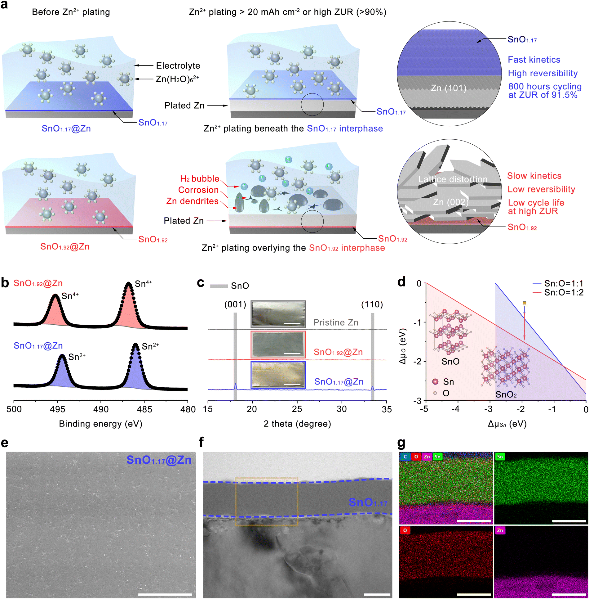 | ||
| Fig. 2 Mechanism of the two different Zn2+ plating behaviors and properties of SnO1.17@Zn. (a) Schematic illustration of the underlying Zn(101) plating and overlying Zn(002) plating relative to the interphase. (b) HR-XPS of Sn 3d for SnO1.92@Zn and SnO1.17@Zn. (c) XRD patterns of pristine Zn, SnO1.92@Zn, and SnO1.17@Zn with insets showing digital photos of the specimens (scale bar, 4 cm). (d) The chemical potential of Sn and O for crystalline SnO and SnO2 with insets showing the crystalline atomic structures of the two Sn–O phases. (e) A plane-view SEM image of SnO1.17@Zn (scale bar, 100 μm). TEM images of (f) a cross-sectional view and (g) the corresponding elemental mapping micrographs of SnO1.17@Zn (scale bar, 50 nm). | ||
Results and discussion
X-ray photoelectron spectroscopy (XPS) surveys (Fig. S2, ESI†) with binding energies (BE) ranging from 0 to 900 eV show similar spectra to each other, in which Sn 3d and O 1s peaks are observed with other Sn-related peaks from Sn 3s, 3p, 4s, and 4d excitations. High-resolution XPS (HR-XPS) investigations were performed to analyze the elemental compositions and the valence state of major elements in both SnO1.92 and SnO1.17 artificial interphases. SnO1.17 exhibits two major spin–orbit split pairs of Sn 3d5/2 at 486.0 eV and Sn 3d3/2 at 494.4 eV, resulting from the Sn2+ state in SnO (Fig. 2(b)). In contrast, the overall peak location of Sn 3d in SnO1.92 shifted toward higher binding energy by approximately 0.8 eV, which is attributed to Sn4+ in SnO2.38 Moreover, the main peak of O 1s in SnO1.92 is located at higher binding energies (ΔBE ∼ 1.6 eV) compared to that in SnO1.17 (Fig. S3, ESI†), suggesting a higher oxidation state. The Sn to O elemental ratios of the two distinct tin oxide films are estimated to be 1:1.92 for the higher oxygen species (SnO1.92) and 1:1.17 for the lower oxygen phase (SnO1.17), respectively through peak area analysis of the HR XPS spectra, indicating slight non-stoichiometric compositions of both phases.
Digital photographs show that the pristine Zn foil turns from shiny silvery to blueish-grey and to pale gold after applying SnO1.92 and SnO1.17 interphases, respectively (the inset of Fig. 2(c)). Homogeneous films were achieved over a large area (12 × 5.5 cm) for both SnO1.92@Zn and SnO1.17@Zn samples, suggesting the viability of mass production for practical applications. The X-ray diffraction (XRD) spectra show that the two modified Zn samples (SnO1.92@Zn and SnO1.17@Zn) well preserve typical metallic Zn, compared to pristine Zn as illustrated in Fig. S4 (ESI†). Noteworthily, two crystalline peaks at the diffraction angles of near 18.1 and 33.4° are observed for SnO1.17@Zn (Fig. 2(c) and Fig. S4, ESI†), which correspond to the (001) and (110) planes of the SnO crystal structure (JCPDS no. 06-0395).39 In contrast, no significant diffraction peaks are observed for SnO1.92@Zn, suggesting the amorphous state of the SnO1.92 interphase.
To understand the mechanism of crystallinity of Sn–O compounds with different stoichiometries, the chemical potential of the Sn–O system was investigated. The growth conditions of the crystalline phases of SnO and SnO2 of each element should satisfy the following thermodynamic conditions (eqn (1) and (2)).
| ΔμSn + Δμ0 = ΔHf,SnO = −2.827 eV | (1) |
| ΔμSn + 2Δμ0 = ΔHf,SnO2 = −4.923 eV | (2) |
Linear sweep voltammetry (LSV) at 5 mVs−1 in 2 M Na2SO4 aqueous electrolyte based on a three-electrode system was employed to characterize the polarization behaviors of pristine and modified Zn anodes to evaluate the efficacy of the stoichiometrically different Sn–O interphases in HER inhibition. The Zn foil, Pt foil, and Ag/AgCl acted as the working electrode, the counter electrode, and the reference electrode, respectively. Without the Zn2+ deposition, the current responses in LSV directly account for HER. The presence of Sn–O compounds decreases the cathodic current density and shifts the potential of the HER at −2 mAcm−2 from −1.30 V on pristine Zn to −1.57 V on SnO1.92@Zn and −1.78 V on SnO1.17@Zn (vs. Ag/AgCl) as indicated by the dashed lines in Fig. 3(a). This confirms the stronger resistance of SnO1.17 to the HER. Cyclic voltammetry (CV) was used to verify the compatibility and effect of the Sn–O interphase on the electrochemical deposition of Zn2+. As shown in Fig. 3(b), the oxidation and reduction peaks of Zn||Ti cells appear only when Zn2+ stripping/plating occurs, which suggests the electrochemical activity of Zn2+ through the Sn–O interphase. The reduction potential increased from B (pristine) to B′ (with SnO1.92) and B′′ (with SnO1.17), signifying that SnO1.17 has a better ability to enable the rapid transfer of Zn2+ and to alleviate the concentration polarization during Zn2+ plating. The higher current densities observed in the SnO1.92@Zn and pristine Zn anodes are attributed to parasitic reactions, such as the HER and corrosion, which contribute to the overall reaction current densities.24,45 Tafel plots in Fig. 3(c) confirm a decreased corrosion current of 3.4 mAcm−2 on SnO1.17@Zn, which is much lower than that of pristine Zn (17.8 mAcm−2) and SnO1.92@Zn (7.6 mAcm−2). These results demonstrate that the SnO1.17 interphase shows a stronger resistance to the HER and Zn corrosion than SnO1.92. The chronoamperometry (CA) investigations in Fig. 3(d) provide insights into the Zn2+ plating mechanisms of the pristine and modified anodes. The current density with the pristine Zn continuously increases, suggesting a long rampant 2D Zn diffusion process, during which Zn2+ tends to accumulate at the tip of the Zn anode and generate dendrites.46,47 In contrast, the current reaches a steady state after about 100 s for SnO1.17@Zn and 200 s for SnO1.92@Zn, which indicates that the Zn2+ diffusion shifts to stable 3D diffusion after a short 2D diffusion, resulting in dense Zn nucleation sites and smooth deposition morphology. This result suggests that the SnO1.17 interphase establishes the rapid stabilization of the Zn2+ diffusion process more effectively than SnO1.92. In addition, the activation energy (Ea) for charge transfer resistance (Rct) estimated from the Arrhenius equation (Fig. 2(e) and Fig. S9, ESI†) allows for the identification of the de-solvation capability of each electrode. Notably, SnO1.17@Zn exhibits a significantly lower Ea of 30.6 kJ mol−1 compared to 41.8 kJ mol−1 for pristine Zn and 35.7 kJ mol−1 for SnO1.92@Zn. These results indicate that the de-solvation process of Zn2+ is more facile on SnO1.17 than on SnO1.92 and pristine Zn, resulting in improved kinetic conditions. The Zn2+ transference number (tZn2+) is measured to evaluate the Zn2+ diffusion ability of the Sn–O interphase (Fig. 3(f)). Based on the CA and electrochemical impedance spectroscopy (EIS) tests (Fig. S10, ESI†), SnO1.17@Zn exhibits a tZn2+ of 0.86 in Fig. 3(f), which significantly surpasses those of pristine Zn (tZn2+ = 0.41) and SnO1.92@Zn (tZn2+ = 0.67), The higher tZn2+ ensures a more efficient transfer of Zn2+ while restricting the migration of SO42− anions, ultimately contributing to uniform Zn2+ plating due to the mitigated concentration polarization.48
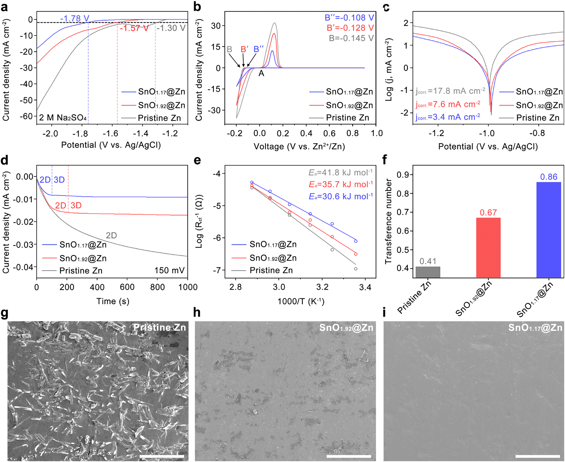 | ||
| Fig. 3 Effects of the Sn–O interphase on water erosion and kinetics of Zn2+ plating/stripping. (a) HER polarization curves of pristine Zn, SnO1.92@Zn, and SnO1.17@Zn in 2 M Na2SO4 aqueous electrolyte at 5 mV s−1. (b) CV of Zn nucleation on pristine Zn, SnO1.92@Zn, and SnO1.17@Zn at the scan rate of 10 mV s−1. (c) Tafel plots of pristine Zn, SnO1.92@Zn, and SnO1.17@Zn. (d) Chronoamperograms of pristine Zn, SnO1.92@Zn, and SnO1.17@Zn anodes. (e) Arrhenius curves of pristine Zn, SnO1.92@Zn, and SnO1.92@Zn anodes. (f) Zn2+ transference numbers of pristine Zn, SnO1.92@Zn, and SnO1.17@Zn. SEM images of (g) pristine Zn, (h) SnO1.92@Zn, and (i) SnO1.17@Zn anodes soaked in 2 M ZnSO4 aqueous electrolyte for 5 days (scale bar, 20 μm). | ||
In addition to the contact angle hydrophobicity measurements shown in Fig. S8 (ESI†), the endurance of the SnO1.17 interphase to water-induced erosion was further investigated. Pristine Zn, SnO1.92@Zn, and SnO1.17@Zn anodes were soaked in 2 M ZnSO4 aqueous electrolyte for 5 days. As shown in a SEM microstructure, Fig. 3(g), numerous rod-like products accumulated on the surface of the pristine Zn anode, identified as Zn4SO4(OH)6·5H2O based on XRD results (Fig. S11, ESI†). The formation of Zn4SO4(OH)6·5H2O is known to be induced by the HER on Zn, which elevates the local pH near Zn, thereby triggering the precipitation of by-products.49 In contrast, minor Zn4SO4(OH)6·5H2O peaks are observed in SnO1.92@Zn, while they are entirely absent in SnO1.17@Zn as shown in Fig. S11 (ESI†). The SEM microstructure of SnO1.92@Zn (Fig. 3(h)) reveals identifiable by-products on the surface, whereas the SnO1.17@Zn surface (Fig. 3(i)) remains compact and uniform without any by-products, consistent with the XRD results (Fig. S11, ESI†), suggesting the effective inhibition of water erosion on SnO1.17@Zn.
The effect of the SnO1.17 and SnO1.92 interphases on the electrochemical performance of the Zn anode was investigated using symmetric Zn cells. As shown in Fig. 4(a), the SnO1.17@Zn symmetric cell exhibits cycling stability over 3000 h at 1 mA cm−2 and 1 mA h cm−2 with a much lower overpotential of 33 mV, which is about 2 and 11 times longer lifespan compared to SnO1.92@Zn (overpotential: 54 mV) and pristine Zn (overpotential: 58 mV), respectively. Optical images of symmetric cells after cycling demonstrate a significant reduction in HER activity during long-term cycling (>3000 h) due to the presence of the SnO1.17 interphase (Fig. S12, ESI†). In addition, at 5 mA cm−2 and 5 mA h cm−2 (Fig. S13, ESI†), the SnO1.17@Zn symmetric cell showed high stability over 1500 h and a lower overpotential of 61 mV, which surpasses the pristine Zn (∼190 h, 128 mV) and SnO1.92@Zn (∼700 h, 92 mV) cells. Additionally, SEM images of the cycled electrodes (Fig. S14, ESI†) show that the SnO1.17@Zn electrode maintains a compact and uniform surface, in contrast to the higher roughness and by-products formed on SnO1.92@Zn and pristine Zn. These microstructure comparisons suggest that SnO1.17, as the anode interface modifier, exhibits a strong capability to restrict the dendrite formation during the Zn2+ plating/stripping process. Notably, even at the high current density of 20 mA cm−2 with 20 mA h cm−2 (Fig. 4(b)), the SnO1.17@Zn symmetric cell still sustains stable cycling over 600 h with a relatively low overpotential of 72 mV, which corresponds to a ZUR as high as 85.72%. In contrast, the SnO1.92@Zn symmetric cell retained stable cycling only for approximately 140 hours with a larger overpotential of 124 mV, while the pristine Zn cell experienced a short circuit after only about 40 hours. To realize the low N/P ratio for practical applications, an ultrathin Zn (UT Zn) anode with a thickness of around 2.8 μm, which corresponds to an areal capacity of 1.63 mA h cm−2, was made by thermal evaporation. The UT Zn anodes were cycled at 1.5 mA cm−2 with 1.5 mA h cm−2, equivalent to a ZUR of ∼91.5% as indicated in Fig. S14 (ESI†). The SnO1.17@UT Zn symmetric cell stably cycled for 800 h with a low overpotential of 43 mV compared to the ∼350 h for the SnO1.92@UT Zn (68 mV) and the ∼70 h for the pristine UT Zn anodes (76 mV), respectively. This confirms that SnO1.17 could promote Zn2+ transfer kinetics and enhance cycling stability even at large current densities and high ZURs. Zn||Cu asymmetric cells were adopted to evaluate the Zn2+ plating/striping reversibility. The lower nucleation overpotential of SnO1.17@Zn at the initial cycle indicates the promoted Zn reaction kinetics (Fig. S16, ESI†). As shown in Fig. 4(c), the SnO1.17@Zn cell exhibits a higher initial coulombic efficiency (CE) of 96.38% and a higher average CE of 99.87%, compared to the pristine Zn (initial CE: 85.47%, average CE: 90.46%) and SnO1.92@Zn (initial CE: 93.52%, average CE: 99.66%). The average CE of 99.87% measured at 5 mA cm−2 is comparable to 99.83% obtained at 0.1 mA cm−2, indicating the high reversibility of the SnO1.17@Zn anode as indicated in Fig. S17a (ESI†). Additionally, the Aurbach method was employed to eliminate the influence of conversion reactions between Zn metal and the Cu substrate surface, ensuring a more precise determination of the CE. Using this method, the average CE of SnO1.17@Zn was determined to be 99.89%, as shown in Fig. S17b (ESI†), further confirming the highly reversible Zn plating/stripping process. The selected voltage profiles of SnO1.92@Zn (Fig. 4(d)) show the larger polarization potential between each charge and discharge process compared to those of SnO1.17@Zn (Fig. 4(e)), which suggests a facilitated Zn plating process in SnO1.17@Zn. Fig. S18 (ESI†) shows that the pristine Zn cell displays unstable cycling behavior after only 50 cycles, with fluctuating voltage profiles attributed to severe water erosion and dendrite growth on the pristine Zn anode. Fig. 4(f) demonstrates the rate capacities of Zn||Cu asymmetric cells. SnO1.17@Zn displays a higher average CE of over 99.50% with an areal capacity of 5 mA h cm−2 compared to 99.23% for SnO1.92@Zn. The pristine Zn cell experienced a short circuit after only 12 cycles, indicating severe non-uniform Zn plating behavior on the surface of bare Zn. These results confirm that the capability of SnO1.17 to stabilize the electrodeposition of Zn2+ is not limited to low current densities but extended to a much higher density, particularly promising for high-power Zn batteries. Fig. 4(g) presents a comprehensive comparison between this work and reported Zn electrodes with various artificial protection layers in terms of four key parameters (i.e., areal capacity, ZUR, cycle number, and current density). Notably, this work leveraging the anti-corrosion ability and favorable Zn2+ transfer kinetics of SnO1.17 contributed to the significantly extended cycle lives at a 85.7% ZUR for 600 hours at 20 mA cm−2 and 20 mA h cm−2 as well as at a 91.5% ZUR for 800 hours, outperforming previously reported results with generally less than 500 hours, as indicated in Table S4 (ESI†).
 | ||
| Fig. 4 Electrochemical performance of the Zn||Zn and Zn||Cu half cells. Galvanostatic cycling performance of pristine Zn, SnO1.92@Zn, and SnO1.17@Zn based on symmetric Zn||Zn cells at (a) 1 mA cm−2, 1 mA h cm−2 and (b) 20 mA cm−2, 20 mA h cm−2. (c) Galvanostatic cycling performance of pristine Cu, SnO1.92@Cu, and SnO1.17@Cu based on asymmetric Zn||Cu cells at 10 mA cm−2 and 5 mA h cm−2. Voltage–capacity curves at different cycles of asymmetric Zn||Cu cells with (d) the SnO1.92 interphase and (e) the SnO1.17 interphase. (f) Rate capacities of asymmetric Zn||Cu cells at an areal capacity of 5 mA h cm−2 and current densities from 5 to 80mAcm−2. (g) Comprehensive comparison of the SnO1.17@Zn anode with recently reported Zn anodes. | ||
The electrodeposition behavior of Zn2+ was characterized to identify the mechanism responsible for the stability difference between SnO1.17@Zn and SnO1.92@Zn during electrochemical testing. An optical microscopy system was developed to monitor the behavior of substantial Zn2+ plating (>20 mA h cm−2) in transparent Zn||Zn cells at a current density of 5 mA cm−2in situ. Uneven Zn nucleation sites emerge only after 15 min in pristine Zn and gradually develop into dendritic and Zn protrusions (white circles in Fig. S19, ESI†) on the electrode surface with further plating. In contrast, the in situ optical images in Fig. 5(a) (SnO1.92@Zn) and 5(b) (SnO1.17@Zn) show that the plated Zn (marked with a white dashed line) was uniformly distributed in the initial 4 hours. However, after 4 hours, the Zn2+ plating layer in SnO1.92@Zn becomes thicker (∼48 μm) than the 38 μm-thick layer in SnO1.17@Zn. This thickness difference may be attributed to the growth of uneven and random Zn protrusion, resulting in looser Zn2+ plating in SnO1.92@Zn. Moreover, the thickness of the Zn2+ plating layer in SnO1.17@Zn is close to the theoretical thickness of Zn2+ plating at 5 mA cm−2 for 4 hours (∼34 μm; Note S1 in the ESI†), suggesting a highly dense Zn2+ plating layer formed with SnO1.17@Zn. Subsequent Zn2+ plating (after 6 hours and 8 hours) in SnO1.92@Zn further increased the surface roughness, resulting in the formation of Zn protrusions. In contrast, the SnO1.17@Zn interphase layer ensures homogeneous and more compact Zn2+ plating throughout the entire 8-hour plating process.
 | ||
| Fig. 5 Comparison of Zn2+ plating behavior between SnO1.92@Zn and SnO1.17@Zn. In situ optical microscopy visualization of Zn2+ plating on (a) SnO1.92@Zn and (b) SnO1.17@Zn at 5 mA cm−2 (scale bar, 100 μm). Three-dimensional confocal laser microscopy images and EDX analysis of Zn2+ plating on (c) SnO1.92@Zn and (d) SnO1.17@Zn for 8 h. (e) Schematic illustration of the overlying and underlying Zn2+ plating of the Sn–O interphase. XRD patterns with the corresponding texture coefficients of (f) SnO1.92@UT Zn and (g) SnO1.17@UT Zn cycled at 1.5 mA cm−2 and 1.5 mA h cm−2 for different times. SEM images of (h) SnO1.92@UT Zn and (i) SnO1.17@UT Zn cycled at 1.5 mA cm−2 and 1.5 mA h cm−2 for different times (scale bar, 10 μm). | ||
Moreover, the confocal laser microscope was employed to quantitively estimate the topological morphology and roughness of the Zn2+ plating layer. Fig. 4(c) and (d) reveal a significant difference in surface roughness (arithmetic mean height, abbreviated as Sa) between SnO1.92@Zn and SnO1.17@Zn after 8 hours. SnO1.92@Zn exhibits a Sa of 5.52 μm, which is more than three times the value of 1.61 μm obtained for SnO1.17@Zn, indicating the uneven Zn2+ plating at a high Zn2+ plating amount (>20 mA h cm−2) in SnO1.92@Zn. The surface roughness of pristine Zn after 1 hour Zn plating is 10.02 μm (Fig. S20, ESI†), critically rougher than those of the modified anodes with a longer duration.
Optical photographs in Fig. S21a–c (ESI†) show different colors of the Zn-plated regions of pristine Zn, SnO1.92@Zn, and SnO1.17@Zn. For the pristine Zn, the apparent color of plated Zn is different from that of pure metallic Zn (initial, not plated). This difference is attributed to the fact that the plated Zn has not undergone polishing, resulting in the absence of metallic shine. Notably, the SnO1.17 interphase exhibits a visible transparency of approximately 50%, as demonstrated by the clear visibility of the “Purdue” logo (Fig. S21d and inset, ESI†), which allows the Zn2+-plated region to remain observable even when located underlying the SnO1.17-coated glass coverslip. EDX was conducted to further analyze the elemental compositions of coated layers. In the EDX spectrum of SnO1.17@Zn (Fig. 5(d)), the characteristic peaks of the element Sn were detected as well as the Zn peaks, whereas no Sn-related peaks were observed in the EDX spectrum of the SnO1.92@Zn sample (Fig. 5(c)), confirming the Zn2+ plating underlying the SnO1.17 interphase, while overlying the SnO1.92 interphase of each modification layer. From further analysis of the elemental weight ratio obtained from EDX (Fig. S22 (ESI†)), the ratio of Sn to O in the SnO1.17@Zn sample was estimated to be 1:1.22, which is close to 1:1.17 for the SnO1.17 interphase. The slightly higher O content may be attributed to the residual of SO42− in the electrolyte and the adsorbed O2 from the air or detection resolution differences between EDX and XPS. The cross-sectional SEM images and EDX elemental mapping of Sn and Zn for the SnO1.17@Zn anode, after Zn2+ plating at ∼2 mA h cm−2, directly confirm that the plated Zn is located beneath the SnO1.17 interphase, as shown in Fig. S23 (ESI†). XRD was employed to further analyze the amorphous/crystalline structure of these Sn–O layers after plating. Two peaks are observed at identical diffraction angles of around 18.1 and 33.4° for plated SnO1.17@Zn as shown in Fig. S24 (ESI†), which correspond to SnO(001) and (110) as discussed in Fig. 2(c), further validating Zn plating beneath SnO1.17 as shown in Fig. 5(e). The in situ observations combined with EDX and XRD also provide strong evidence of both Sn–O interphases controlling the Zn nucleation and growth when the Zn2+ plating amount is below 20 mA h cm−2 (from 0 to 4 hours). Noteworthily, only the SnO1.17 interphase layer can facilitate the formation of a compact and uniform Zn-plated layer from 4 to 8 hours of Zn2+ plating (>20 mA h cm−2). Unlike the SnO1.17 interphase, the SnO1.92 interphase, despite its higher Young's modulus of 207 GPa, does not play any role in suppressing Zn dendrite formation since Zn2+ is plated above the SnO1.92 interphase. This reveals the limitations of SnO1.92 in managing dendrite growth. These results explain the failure process of SnO1.92@Zn at a high plating amount with a low ZUR of ∼30%.
Furthermore, SnO1.17@UT Zn and SnO1.92@UT Zn anodes in symmetric Zn||Zn cells at different cycling times were characterized by XRD (Fig. 5(f) and (g)), with aim of understanding the failure mechanism of the SnO1.92@UT Zn anode at a high ZUR of 91.5% with a low Zn plating amount of 1.5 mA h cm−2 presented earlier in Fig. S15 (ESI†). Peaks at 36.3, 38.9, 43.2, 54.3, 70.1, and 70.7° are observed for both SnO1.92@Zn and SnO1.17@Zn, which are attributed to the plated Zn. The relative texture coefficient of each plane (Tc, Note 2 in ESI†), representing the preferential growth of a particular plane, was calculated to quantify the phase evolution of the plated Zn. As shown in the right of Fig. 5(f) for SnO1.92@Zn, the Tc of the Zn (002) plane at 10 and 100 hours is 83.1 and 84.1 respectively, which is higher than 31.8 and 67.6 for the (101) plane. The Tc comparison indicates that a higher amount of (002)-oriented Zn is plated on the SnO1.92 interphase during the initial cycling. Note that, however, the still exposed Zn(101) in the electrolyte continuously reacts with water due to its higher reactivity than Zn (002), which aggravated the HER and corrosion reactions, contributing to the accumulation of Zn4SO4(OH)6·5H2O (marked as yellow diamonds in Fig. 5(f)). The accumulation of by-products deactivates the ability of the SnO1.92 interphase to induce Zn(002) plating. Subsequently, the Tc of Zn(002) decreased to 55.1 after 200 hours and to even 34.8 after 300 hours, while the Tc of Zn(101) increased to 80.2 and 96.1 after 200 and 300 hours respectively, due to the faster growth rate of Zn(101) than (002). Consequently, the inevitable HER and corrosion reactions with the exposed Zn(101) in SnO1.92@Zn lead to anode failure. In contrast, the Tc of Zn(002) and Tc of Zn(101) in SnO1.17@Zn in Fig. 5(g) (right) were retained until 300 hours, suggesting a highly reversible Zn2+ plating/stripping process at a high ZUR of 91.5%. Noteworthily, the Tc of Zn(101) plated under the SnO1.17 interphase is significantly higher than the Tc of Zn(002) in the entire cycling, indicating the Zn2+ plating preferentially along the (101) plane. The faster mass (Zn2+) transfer of the Zn(101) plane contributes to a lower overpotential during the Zn2+ plating, compared to the (002)-oriented growth of Zn in SnO1.92@Zn.
Fig. 5(h) shows the evolution of the surface morphology of SnO1.92@Zn at different cycling times. Initially, a smooth and compact surface was preserved, as observed at 10 hours of cycling, where the SnO1.92 interphase benefits uniform Zn2+ plating and inhibits the parasitic reactions within the initial 10 hours. However, it is noticed that the surface roughness increased at 100 hours of cycles with several pores (marked with white arrows) generated, which may reduce the compactness of the Zn2+ plating layer and lead to the penetration of the water, triggering the mechanical failure and the water corrosion of SnO1.92@Zn. As the cycling further proceeded for 200 hours, the roughness of the surface regions of SnO1.92@Zn increased drastically with the protrusions and cavities (marked with white arrows). Besides, the pore size increased from hundreds of nanometers to several micrometers, which would lead to a more severe HER and corrosion reaction, which was further confirmed by the SEM image of SnO1.92@Zn cycled for 300 hours. A lot of by-products (marked with white dashed lines) derived from the water corrosion process can be identified, resulting in the rapid failure of electrochemical performance. In contrast, the surface morphology of SnO1.17@Zn remained compact and smooth throughout the entire process. The (101)-oriented Zn plated underlying SnO1.17 was shielded from direct exposure to water molecules by the SnO1.17 interphase, protecting it from corrosion and the HER, resulting in a fast and reversible Zn2+ plating/stripping process.
Additionally, a combination of experimental and theoretical methods was employed to further understand the Zn2+ plating behaviors (position and crystalline orientation) as a function of Sn–O phases. According to the widely accepted ion deposition mechanism, the Zn2+ plating process is generally understood to involve three steps: Zn2+ adsorption, Zn2+ diffusion, and Zn2+ reduction.50 Density functional theory (DFT) was employed to evaluate the adsorption capabilities of the Zn atom by calculating the selected sites on pristine Zn, SnO1.17, and SnO1.92 as shown in Fig. S25 and Table S5 (ESI†).
As indicated in Fig. 6(a), the Zn atom tends to adsorb on the hollow site on the (101) plane (site 4) with the lowest adsorption energy of −1.42 eV in pristine Zn. For SnO1.17, the Zn atom thermodynamically prefers adsorption on the hollow site between two O atoms on the (101) plane (site 6) owing to the lower energy of −2.48 eV. SnO1.92 shows an overall stronger adsorption tendency (−3.22 to −3.71 eV) towards the Zn atom with the most preferable Zn adsorption on top of the O atom (site 3; −3.71 eV). The insets show the charge density difference of Zn-site 4, SnO1.17-site 6, and SnO1.92-site 3. Among the three anode systems, Zn metal shows the least tendency to adsorb Zn ions (−1.42 eV), which is accounted for by the weakest (the smallest size of the charge difference density region) charge accumulation (red) and depletion (blue) between the Zn and Zn atoms. In SnO1.17-site 6 and SnO1.92-site 3, the electrons are strongly depleted around the Zn atom, while electrons accumulate around the O adjunct of the Zn atom, suggesting a strong tendency of the Zn atom to donate electrons. Noteworthily, the charge accumulation and depletion regions in SnO1.92-site 3 are more prominent than those in SnO1.17-site 6, resulting in stronger adsorption. It should be noted that strong adsorption may reduce the Zn nucleation overpotential and improve the uniform Zn deposition but may not lead to the facilitated Zn transport on the anode surface. However, weak adsorption is not beneficial for promoting uniform nucleation and deposition but is always accompanied by a low migration energy barrier, which can achieve fast Zn transport. SnO1.17 with moderate adsorption capabilities may achieve an optimization between the Zn nucleation overpotential and Zn transport kinetics compared to metallic Zn and the one with the SnO1.92 interphase. An optimal Zn2+ adsorption strength of SnO1.17 secures both uniform Zn2+ plating and fast ion transport on the anode, as proved by electrochemical analysis in Fig. 3 and 4.
 | ||
| Fig. 6 Mechanistic understanding of the effect of SnO1.17 and SnO1.92 interphases on Zn2+ plating. (a) Adsorption energy of the Zn atoms on Zn, SnO1.17, and SnO1.92. Insets show the charge density differences of Zn-site 4, SnO1.17-site 6, and SnO1.92-site 3. (b) MEPs (right) obtained from NEB calculations and the corresponding diffusion energy barrier (left) for Zn2+ diffusion through SnO1.92 and SnO1.17. (c) I–V curves of SnO1.92@Zn (red) and SnO1.17@Zn (blue). Insets show schematic illustration of the band diagrams of SnO1.92/Zn (top) and SnO1.17/Zn (bottom). (d) Surface energies of Zn(002) and Zn(101) with SnO1.17 and SnO1.92 interphases. (e) The pDOS of Zn 4s and O 2p orbitals of SnO1.17@Zn and SnO1.92@Zn. (f) Simulated results of Zn2+ concentration of pristine Zn, Ohmic contact of SnO1.92@Zn, and Schottky contact of SnO1.17@Zn. (g) Schematic of the correlation between the energy barrier of Zn2+ and the specific diffusion in the OHP, IHP, and solid phase of pristine Zn, SnO1.92@Zn, and SnO1.17@Zn. | ||
The migration energy barriers for Zn2+ near the most stable adsorption sites of SnO1.17 and SnO1.92 were calculated using the climbing image nudged elastic band (NEB) method.51,52Fig. 6(b) shows that the migration energy barrier of Zn2+ in SnO1.92 is about 1.59 eV, and this high energy barrier indicates a slow transport of Zn2+, leading to the sluggish Zn2+ plating/stripping behavior. However, Zn2+ is able to more easily migrate along the (110) and (001) planes of SnO1.17 due to the significantly lower energy barriers of 0.66 and 0.32 eV. The Zn2+ migration along the interface of the (110) and (001) planes needs to be considered as well due to the fast kinetics of Zn2+.53 It should be noted that the grain boundary between (101) and (001) planes (path 3 in SnO1.17) is identified to be the fastest Zn2+ transport path with the lowest barrier energy of 0.16 eV. Fig. 6(b) and Fig. S26 (ESI†) illustrate the minimum energy path (MEP) of Zn2+ connecting the initial and final states of SnO1.17 and SnO1.92. SnO1.92 shows a much narrower Zn2+ transport channel with an average distance of 1.62 Å between Zn and O, which contributes to stronger Zn–O interactions and a resultant higher migration energy barrier, compared to 1.78 Å for path 1, 1.91 Å for path 2, and 2.23 Å for path 3 in SnO1.17. Additionally, the MEP of SnO1.92 that involves seven O atoms experiences more interactions between Zn and O during the Zn2+ migration, which hence results in slow Zn2+ transport. In contrast, SnO1.17 engaging less O atoms (four in path 1, six in path 2, and five in path 3) facilitates the Zn2+ migration with a higher ionic conductivity of 1.36 × 10⁻⁴ mS cm−1, compared to 8.72 × 10⁻⁷ mS cm−1 for SnO1.92, as measured in Fig. S27 (ESI†). Consequently, excessively strong adsorption and a large migration energy barrier of SnO1.92 may impede the diffusion of Zn2+ into the bulk Zn. However, SnO1.17 is considered to be more suitable for Zn2+ diffusion due to the favorable kinetics, which is a prerequisite for Zn2+ plating underlying the SnO1.17 interphase.
The electrostatic interaction between the Sn–O interphase and the Zn foil was investigated to unveil the effect of Sn–O interphases on the inner Helmholtz plane (IHP), which is crucial for determining the morphology of Zn plating and parasitic reactions. Current–voltage (I–V) behaviors of the symmetric cells of Zn|SnO1.17|Zn and Zn|SnO1.92|Zn (without electrolyte) were characterized to verify the electrostatic interactions at the interface between each Sn–O interphase and the Zn metal, and the results are shown in Fig. 6(c). A linear increased I–V curve of the SnO1.92/Zn contact implies an Ohmic behavior and a continuous electron transfer across the interface within the applied voltage range from −1.5 to 1.5 V, leading to an areal current density higher than 0.4 mA cm−2. In contrast, the absolute value of the current density of Zn|SnO1.17|Zn is lower than 5 μA cm−2 within −1.5 and 1.5 V, which suggests that electron transport is significantly limited at the SnO1.17/Zn interface. Besides, the measured I–V characteristic indicates the non-linear behavior at the SnO1.17/Zn interface (Fig. S28, ESI†). The different electrostatic behaviors at the interface are attributed to the distinct band alignments at the Sn–O phase-dominated interface and the types of majority carriers. The majority carrier of SnO1.17 has been identified as holes (i.e., p-type) with a work function of 5.42 eV, as shown in Fig. S29 (ESI†).39 SnO1.17 forms a Schottky contact with Zn metal (ΦZn: ∼4.3 eV) with a Schottky energy barrier (ΦB), which is the required energy for carrier conduction and estimated to be 1.1 eV from the difference between the work functions (i.e., ΦSnO1.17 − ΦZn). This non-Ohmic contact would create a charge depletion region in SnO1.17 near the interface, limiting the charge carrier transport within the Zn metal during the Zn2+ plating/stripping process. Besides, the p-type SnO1.17 has a positively charged environment, which delays the electron reception of Zn2+ within the SnO1.17 interphase until the Zn2+ reaches the Zn anode (i.e., at the SnO1.17/Zn interface), enabling the Zn2+ reduction beneath the SnO1.17 interphase.54 Conversely, electrons work as the majority carriers (i.e., n-type) in SnO1.92 with a work function of 4.53 eV.55 The contact of SnO1.92 and Zn metal could facilitate electron transfer since there is no energy barrier for electron flow between SnO1.92 and Zn metal, which induces electron accumulation at the surface of SnO1.92 in the Zn2+ plating process. The electrostatic interaction between Sn and O interphases and Cu foil was also tested to understand the origin of the compelling performance of the SnO1.17@Cu anode in Zn||Cu asymmetric cells (Fig. S30, ESI†). Similar to the contacts with Zn, Schottky behavior was also observed when SnO1.17 was in contact with Cu metal, while Ohmic behavior occurred in SnO1.92 with Cu metal. Consequently, charge carrier transport is restricted to the Cu metal in SnO1.17@Cu during Zn2+ stripping/plating, by which the reduction location for Zn2+ was altered underlying the SnO1.17 interphase. However, the electron transfer at the SnO1.92/Cu interface was facilitated by the Ohmic contact.
The capacitance of the non-faradaic electric double layer (EDL) was measured via alternating current (AC) voltammetry to quantify the effect of SnO1.17 and SnO1.92 on the ion distribution in IHP. The voltage range of the non-faradaic region was identified as 0.6–0.9 V (vs. Zn2+/Zn) according to the CV measurement (Fig. S31, ESI†). As shown in Fig. S32 (ESI†), the capacitance value of 7.23 μF of the cell with SnO1.17 is lower than 12.32 μF for the cell with SnO1.92 and 14.42 μF for the pristine sample, which was ascribed to the weaker EDL with the increased distance between the negatively charged surface and IHP. These results suggest that appropriate band alignment through work function engineering may promote the Zn2+ migration within IHP as demonstrated in the modified Zn anode surface, i.e., SnO1.17/Zn metal. As a result, the Zn2+ migrates through the SnO1.17 interphase and is reduced to Zn0 when receiving electrons from Zn metal, inducing the Zn2+ plating beneath SnO1.17. In contrast, with the high Zn2+ migration barrier for SnO1.92 and the sufficient electrons supplied by the Ohmic SnO1.92/Zn contact, Zn2+ tends to be plated on top of the SnO1.92 surface.
To further identify the underlying mechanism of the preferential crystalline orientation of Zn electroplating and morphology regulation by Sn–O interphases, the variation of the surface energy of the (002) and (101) planes before and after integrating with Sn–O interphases has been calculated (Fig. 6(d)). The Zn(101) plane exhibited a high surface energy of 1.65 J m−2 due to the presence of Zn dangling bonds at the surface, making it challenging to achieve well-aligned Zn(101) plating. The surface energy of the Zn(101) plane decreased from 1.65 J m−2 (in pristine Zn) to 0.74 J m−2 when the SnO1.17 interphase was applied, resulting in reduced Zn(101) nucleation resistance. Even the Zn(002) and (101) planes have similar surface energy after applying the SnO1.17 interphase; the Zn(101) plane will cover the (002) plane due to the faster growth rate, leading to the high ratio of the well-aligned Zn (101) plane. The SnO1.92 interphase drastically reduces the surface energy of Zn(002) from 0.88 J m−2 (in pristine Zn) to 0.30 J m−2, promoting the preferential growth of the Zn(002) plane. The projected density of states (pDOS) was calculated to elucidate why SnO1.17 and SnO1.92 have different effects on reducing surface energy. As shown in Fig. 6(e), SnO1.17 exhibits strong affinity towards the Zn atoms of the (101) plane due to the obvious overlap between the O 2p orbital and the Zn 4s orbital, while only weak pDOS overlap between Zn 4s of the (002) plane and O 2p. In contrast, a strong pDOS overlap between Zn 4s of the Zn (002) plane and O 2p is observed when the SnO1.92 interphase is applied, as illustrated in Fig. 6(e), indicating a prominent interaction between SnO1.92 and the Zn(002) plane. Besides, only faint pDOS overlaps were observed between O 2p and Zn 4s of Zn(101), suggesting a much weaker interaction between SnO1.92 and the Zn(101) plane. In summary, the SnO1.17 interphase could saturate the Zn dangling bonds on the surface of Zn(101), resulting in the formation of dative bonds, thus significantly reducing the surface energy of the Zn(101) plane and hence leading to the preferential growth of Zn(101). However, the SnO1.92 interphase decreased the surface energy of Zn(002) by strong interactions between O and Zn atoms of the (002) plane, facilitating the growth of (002) orientation.
Finite element analysis was carried out to visualize the concentration distribution of Zn2+ in cells with pristine Zn, SnO1.92@Zn, and SnO1.17@Zn at 0.5 V. As illustrated in Fig. 6(f), pristine Zn exhibited the highest Zn2+ concentration gradient, compared to the SnO1.92@Zn and SnO1.17@Zn, which was ascribed to the high electric field region on the tip of Zn metal as shown in Fig. S34 (ESI†). In the case of SnO1.92@Zn and SnO1.17@Zn, Ohmic and Schottky contact was built to reflect the charge carrier transmission and inhibition characteristics at the interface between the Sn–O interphase and Zn metal. The SnO1.92@Zn exhibits a higher Zn2+ concentration gradient above the SnO1.92 interphase compared to that above the SnO1.17 interphase in SnO1.17@Zn, corresponding to the stronger EDL presented in SnO1.92@Zn. The Zn2+ concentration of SnO1.92@Zn below the Sn–O interphase is drastically decreased due to the limited migration capability of Zn2+ in SnO1.92. Consequently, Zn2+ ions tend to accumulate and undergo reduction by gaining electrons at the surface of the SnO1.92 interphase. In contrast, the Zn2+ concentration beneath the SnO1.17 interphase is similar to that above it, as Zn2+ ions easily migrate in SnO1.17 with a lower energy barrier (as in Fig. 6(a) and (b)) and are subsequently reduced to (101)-oriented Zn underlying the SnO1.17 interphase. As a result, SnO1.17@Zn facilitates rapid Zn2+ diffusion with a lower energy barrier (liquid–solid) and the faster growth rate of Zn (101) plane (solid) as illustrated schematically in Fig. 6(g).
Various cathodes have been adopted to assemble Zn-based full batteries to evaluate the reliability of SnO1.92@Zn and SnO1.17@Zn for practical applications. The cycling stability of the Zn-based full batteries was tested at low rates because the most stringent proof of stability is not necessarily manifested by the number of cycles but rather by the time the system spends in the fully charged state.56,57 The sulfur cathode was selected due to its high specific capacity, leading to a higher ZUR than the other commonly used cathode with the same mass loading. The sulfur cathode was manufactured based on the method reported in our previous research.58 The manufactured PEDOT@S cathodes with a mass loading of around 6 mg cm−2 were coupled with commercialized Zn metal anodes (40 μm), contributing to an N/P ratio of 4.6 at 0.5 A g−1. The PEDOT@S||SnO1.17@Zn cell demonstrates excellent reversibility and rate capability, retaining over 95.2% of its capacity and exhibiting an Rct of 317 Ω after 600 cycles, as shown in Fig. 7(a) and Fig. S35 (ESI†). This performance surpasses that of the PEDOT@S||SnO1.92@Zn battery, which has a capacity retention of 77.4% and an Rct of 487 Ω. The PEDOT@S||Zn battery stably cycled for 334 cycles with a capacity retention of 66.9% and an Rct of 834 Ω before a short circuit occurred at cycle 335 due to the growth of Zn dendrites. The SEM image of pristine Zn after cycling in Fig. S36 (ESI†) exhibits a rough surface with protrusions and cracks, which contributes to the unevenness of Zn2+ plating and severe parasite reactions. Several potholes can be observed on the surface of SnO1.92@Zn, suggesting the inevitable corrosion reaction due to the direct contact between Zn(101) and water. In contrast, the smooth morphology of SnO1.17@Zn after cycling in Fig. S37 (ESI†) indicates superior cycling reversibility. The PEDOT@S||SnO1.17@Zn battery delivered higher capacities at various current densities than the PEDOT@S||SnO1.92@Zn battery and the PEDOT@S||Zn battery, mainly due to faster mass transfer at the (101) Zn orientation in comparison with that at (002) Zn orientation. Moreover, the charge–discharge profiles at different rates in Fig. S37 (ESI†) revealed that the PEDOT@S||SnO1.17@Zn battery show a smaller voltage hysteresis compared with the PEDOT@S||SnO1.92@Zn battery and the PEDOT@S||Zn battery, originating from the facilitated Zn2+ transfer process at SnO1.17@Zn. To further decrease the N/P ratio during the full cell tests, UT Zn (2.8 μm) was employed to pair with the MnO2 cathode, which delivered 225 mA h g−1 when paired with a commercialized Zn anode (40 μm) as shown in Fig. S38 (ESI†), leading to an N/P ratio of 1.26 at a current density of 0.1 A g−1. MnSO4 solution has been added as the electrolyte additive to improve capacity and stability. The MnO2||UT Zn battery underwent a fast degradation at the initial 84 cycles before experiencing a short circuit, which was caused by the accumulation of by-products and Zn dendrite formation due to the uneven Zn2+ plating as identified in Fig. S39 (ESI†). In contrast, the MnO2||SnO1.17@UT Zn battery achieved a capacity retention of 90.5% with an average CE of 99.68% after 400 cycles at 0.1 A g−1, exceeding the capacity retention of 26.4% and an average CE of 98.92% for the MnO2||SnO1.92@UT Zn battery. Moreover, the MnO2||SnO1.17@UT Zn battery demonstrates a lower Rct variation of 21 Ω compared to 30 Ω for the MnO2||SnO1.92@UT Zn battery and 89 Ω for the MnO2||UT Zn as shown in Fig. S40 (ESI†), respectively. The inferior reversibility of the MnO2||SnO1.92@UT Zn battery is mainly attributed to the accumulation of the by-products on the surface of the anode as indicated in Fig. 7(d). The SnO1.17@UT Zn anode shows a smooth surface and a more compact Zn2+ plating layer, verifying the evenness of Zn2+ plating behavior and restricted parasite reactions at SnO1.17@UT Zn. The MnO2||SnO1.17@UT Zn battery exhibits higher specific capacities of 109.6 and 78.9 mA h g−1 at 1 A g−1 and 2 A g−1 as shown in Fig. 7(e), compared to 102.3 and 69.7 mA h g−1 for the MnO2||SnO1.92@UT Zn battery and 97.8 and 59.9 mA h g−1 for the MnO2||UT Zn battery, respectively. This should be related to the favorable Zn2+ transfer process at the anode in the MnO2||SnO1.17@UT Zn battery.
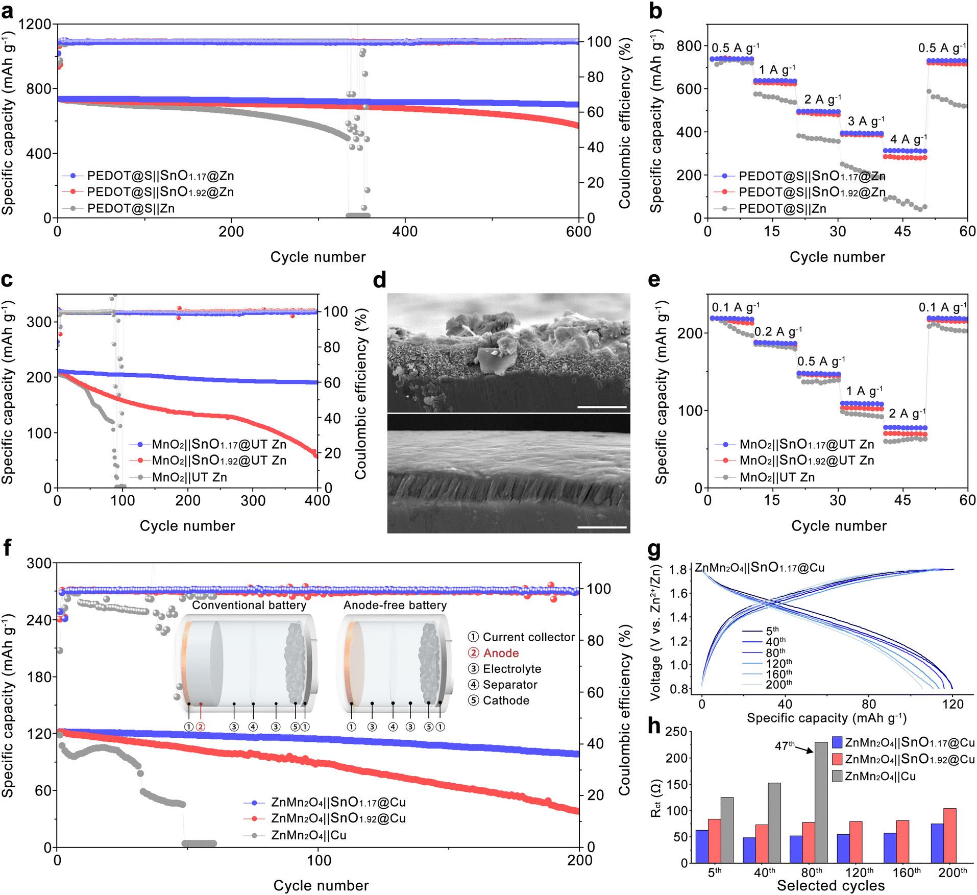 | ||
| Fig. 7 Electrochemical performance of full batteries. (a) Cycling performance and (b) rate performance of the PEDOT@S||Zn batteries with commercialized Zn foils (40 μm); (c) cycling performance of MnO2||Zn cells batteries with UT Zn anodes (2.8 μm); (d) cross-sectional SEM images of cycled SnO1.92@UT Zn (top) and SnO1.17@UT Zn (bottom) (scale bar, 5 μm); (e) rate performance of MnO2||Zn batteries with UT Zn anodes; (f) cycling performance of anode-free ZnMn2O4||Cu with pristine Cu, SnO1.92@Cu, and SnO1.17@Cu. Inset shows the schematic illustration of the conventional Zn-based and anode-free Zn metal batteries. (g) Voltage–capacity curves and (h) charge transfer resistance of the anode-free battery at selected cycles. | ||
As shown in the inset of Fig. 7(f), conventional Zn-based batteries typically use a thick Zn metal foil (100 to 200 μm), leading to a high N/P ratio (60 to 120) within the battery. This not only results in significant material waste but also substantially compromises the energy density at the battery level. However, the configuration of anode-free Zn aqueous batteries represents a promising technique to improve energy density. To achieve the anode-free configuration in the battery, the ZnMn2O4 cathode was chosen to pair with Cu foil as an anode-free Zn aqueous battery, where ZnMn2O4 is the sole source of Zn2+ during cycling. As shown in Fig. S41 (ESI†), the as-synthesized ZnMn2O4 cathode materials delivered a specific capacity of around 155 mA h g−1 at 0.05 A g−1 when paired with conventional Zn foil (40 μm). Then the as-prepared ZnMn2O4 cathode with a mass loading around 2.2 mg cm−2 was coupled with Cu foil, SnO1.92@Cu, and SnO1.17@Cu, respectively, as anode-free batteries. The ZnMn2O4||Cu battery rapidly faded within 47 cycles under these extreme test conditions as shown in Fig. 7(f). However, the ZnMn2O4||SnO1.17@Cu battery retained 81.6% of its original capacity after 200 cycles at 0.1 A g−1, which is much higher than 30.9% for the ZnMn2O4||SnO1.92@Cu battery (Fig. 7(f)). Moreover, the ZnMn2O4||SnO1.17@Cu battery shows a lower voltage decay of 0.03 V, compared to the voltage decay of 0.09 V in the ZnMn2O4||SnO1.92@Cu battery as illustrated in Fig. 7(g) and Fig. S42 (ESI†). The resistance evolution during cycling was evaluated by EIS (Fig. S43, ESI†). The Rct value of the ZnMn2O4||Cu battery drastically increased to 231 Ω at the 47th cycle, which should be ascribed to the accumulation of insulated by-products resulting from the corrosion reactions. In contrast, the Rct value of the ZnMn2O4||SnO1.17@Cu battery remained lower than 80 Ω during the entire cycling process, suggesting the favorable kinetic conditions for Zn2+ plating in the ZnMn2O4||SnO1.17@Cu battery. SEM images further confirm the intensive parasitic reactions occurring during the cycling with vast amounts of by-products accumulated on the surface of the Cu foil, leading to the rapid failure of the ZnMn2O4||Cu battery (Fig. S44, ESI†). There are a lot of micro-caves that can be observed on the surface of SnO1.92@Cu, implying the presence of severe HERs during battery cycling. In contrast, SnO1.17@Cu shows a flat surface without any accumulation of the by-products due to the regulated Zn2+ plating behavior and restricted parasitic reactions, which contributes to the superior cycling performance of the ZnMn2O4||SnO1.17@Cu battery. The successful demonstration of anode-free Zn aqueous batteries verifies the advantages of the SnO1.17 interphase in promoting the edge of the energy density of the Zn-based energy storage devices.
Conclusions
In summary, we successfully induce (101)-oriented Zn2+ plating while spontaneously passivating the plated Zn(101) using a thin SnO1.17 artificial interphase. Further analyses reveal that the electron transfer from the O 2p orbital of the SnO1.17 interphase to the Zn 4s orbital of Zn(101) saturated the Zn dangling bonds at Zn(101), thus lowering the nucleation energy barrier of Zn(101) and leading to the preferential growth of Zn(101). The faster Zn2+ transfer at Zn(101) and high ionic conductivity of the SnO1.17 interphase brought about favorable Zn2+ plating/stripping kinetics, resulting in the lower Zn nucleation overpotential and the smaller voltage hysteresis. In addition, the Zn2+ plating location of the underlying SnO1.17 interphase was determined by synergetic effects of low Zn2+ diffusion barriers and electrostatic electron shielding within the SnO1.17 interphase, which isolates the plated Zn(101) from water molecules, ensuring high reversibility and rapid Zn2+ migration even at elevated ZURs.Consequently, the SnO1.17@Zn symmetric cell operated stably for 600 hours at 20 mA h cm−2 with a ZUR of 85.7% and a lower overpotential of 72 mV compared to the 140 hours and the overpotential of 124 mV for SnO1.92@Zn. The SnO1.17@UT Zn symmetric cell cycled stably for 800 hours with a ZUR of 91.5% and retained 90.5% of its original capacity when paired with an MnO2 cathode in a full cell under low N/P ratio (1.26) conditions. Moreover, the Cu||Zn asymmetric cell modified with the SnO1.17 interphase achieved an average CE of 99.50% at 5 mA cm−2 and 5 mA h cm−2 for 1000 cycles and demonstrated a high-capacity retention of 81.6% after 200 cycles at a low current density of 0.1 A g−1 when applied in an anode-free system. This work outlines the potential of Zn(101) for reversible and kinetically favorable Zn2+ plating/stripping to achieve high ZURs at high current densities for practical ZIBs.
Author contributions
Y. Z. and S. L. conceived the idea, designed the experiments, and wrote and revised the manuscript. Y. Z., M. K., F. Q., and D. H. L. performed experiments and formal analysis. C. S. K., J. P. and C. K. conducted related characterization procedures. F. L. helped with the analysis of the electrochemical data. S. L. supervised the project. H.-W. S. and S. L. provided the funding acquisition. All the authors commented on the manuscript.Data availability
All data that support the findings of this study are available from the corresponding author upon reasonable request.Conflicts of interest
There are no conflicts to declare.Acknowledgements
This work was supported by the US National Science Foundation, Award numbers CBET-2207302 and CMMI-2318677. SL and HWS acknowledge the support from the National Research Council of Science & Technology (NST) grant by the Korea Ministry of Science and ICT (MSIT) (CRC23021-000).Notes and references
- G. Fang, J. Zhou, A. Pan and S. Liang, ACS Energy Lett., 2018, 3, 2480–2501 CAS.
- F. Wang, O. Borodin, T. Gao, X. Fan, W. Sun, F. Han, A. Faraone, J. A. Dura, K. Xu and C. Wang, Nat. Mater., 2018, 17, 543–549 CAS.
- H. Pan, Y. Shao, P. Yan, Y. Cheng, K. S. Han, Z. Nie, C. Wang, J. Yang, X. Li, P. Bhattacharya, K. T. Mueller and J. Liu, Nat. Energy, 2016, 1, 16039 CAS.
- C. Xu, B. Li, H. Du and F. Kang, Angew. Chem., Int. Ed., 2012, 51, 933–935 CAS.
- H. Li, L. Ma, C. Han, Z. Wang, Z. Liu, Z. Tang and C. Zhi, Nano Energy, 2019, 62, 550–587 CAS.
- Z. Zhao, J. Zhao, Z. Hu, J. Li, J. Li, Y. Zhang, C. Wang and G. Cui, Energy Environ. Sci., 2019, 12, 1938–1949 CAS.
- Z. Wu, Y. Wang and C. Zhi, Joule, 2024, 8, 2442–2448 Search PubMed.
- L. Ma, M. A. Schroeder, O. Borodin, T. P. Pollard, M. S. Ding, C. Wang and K. Xu, Nat. Energy, 2020, 5, 743–749 CAS.
- M. Zhou, S. Guo, J. Li, X. Luo, Z. Liu, T. Zhang, X. Cao, M. Long, B. Lu, A. Pan, G. Fang, J. Zhou and S. Liang, Adv. Mater., 2021, 33, 2100187 CAS.
- W. Yuan, X. Nie, G. Ma, M. Liu, Y. Wang, S. Shen and N. Zhang, Angew. Chem., Int. Ed., 2023, 62, e202218386 CAS.
- G. Liu, Y. Tang, Y. Wei, H. Li, J. Yan, Z. Feng, W. Du, Q. Yang, M. Ye, Y. Zhang, Z. Wen, X. Liu and C. C. Li, Angew. Chem., Int. Ed., 2024, e202407639 CAS.
- P. Curie, Bull. Mineral., 1885, 8, 145–150 Search PubMed.
- S. F. Li, X. J. Zhao, X. S. Xu, Y. F. Gao and Z. Zhang, Phys. Rev. Lett., 2013, 111, 115501 CAS.
- S. Chen, K. Ouyang, Y. Liu, M. Cui, G. Pu, Y. Wang, K. Zhang and Y. Huang, Angew. Chem., Int. Ed., 2024, e202409303 CAS.
- X. Zhang, J. Li, Y. Liu, B. Lu, S. Liang and J. Zhou, Nat. Commun., 2024, 15, 2735 CrossRef CAS PubMed.
- H. Zhang, Y. Zhong, J. Li, Y. Liao, J. Zeng, Y. Shen, L. Yuan, Z. Li and Y. Huang, Adv. Energy Mater., 2023, 13, 2203254 CrossRef CAS.
- J. Zheng, Q. Zhao, T. Tang, J. Yin, C. D. Quilty, G. D. Renderos, X. Liu, Y. Deng, L. Wang, D. C. Bock, C. Jaye, D. Zhang, E. S. Takeuchi, K. J. Takeuchi, A. C. Marschilok and L. A. Archer, Science, 2019, 366, 645–648 CrossRef CAS PubMed.
- Y. Wang, X. Xu, J. Yin, G. Huang, T. Guo, Z. Tian, R. Alsaadi, Y. Zhu and H. N. Alshareef, Adv. Mater., 2023, 35, 2208171 CrossRef CAS PubMed.
- Z. Zhang, Y. Wang, J. Sun, L. Dang, Q. Li, X. He, Z. Liu and Z. Lei, Small, 2024, 2402636 CrossRef CAS PubMed.
- R. Yuksel, O. Buyukcakir, W. K. Seong and R. S. Ruoff, Adv. Energy Mater., 2020, 10, 1904215 Search PubMed.
- X. Zhang, J. Li, K. Qi, Y. Yang, D. Liu, T. Wang, S. Liang, B. Lu, Y. Zhu and J. Zhou, Adv. Mater., 2022, 34, 2205175 CrossRef CAS PubMed.
- W. Xie, K. Zhu, W. Jiang, H. Yang, M. Ma, L. Zhao and W. Yang, ACS Nano, 2024, 18, 21184–21197 CrossRef CAS PubMed.
- J. Zhang, W. Huang, L. Li, C. Chang, K. Yang, L. Gao and X. Pu, Adv. Mater., 2023, 35, 2300073 CrossRef CAS PubMed.
- Z. Liu, Z. Guo, L. Fan, C. Zhao, A. Chen, M. Wang, M. Li, X. Lu, J. Zhang, Y. Zhang and N. Zhang, Adv. Mater., 2024, 36, 2305988 CrossRef CAS PubMed.
- Z. Cheng, K. Wang, J. Fu, F. Mo, P. Lu, J. Gao, D. Ho, B. Li and H. Hu, Adv. Energy Mater., 2024, 14, 2304003 CrossRef CAS.
- Y. Zhang, X. Han, R. Liu, Z. Yang, S. Zhang, Y. Zhang, H. Wang, Y. Cao, A. Chen and J. Sun, Small, 2022, 18, 2105978 CrossRef CAS PubMed.
- Y. Su, L. Xu, Y. Sun, W. Guo, X. Yang, Y. Zou, M. Ding, Q. Zhang, C. Qiao, S. Dou, T. Cheng and J. Sun, Small, 2024, 20, 2308209 CrossRef CAS PubMed.
- Y. Wang, C. Chen, A. Xu, J. Lv, M. Huang, T. Ren, J. Bai, H. Wang and X. Liu, Adv. Energy Mater., 2024, 2404071 CrossRef.
- Q. Ren, X. Tang, Y. Guo, X. Liao, C. Zhang, Z. Zhu, P. Wang, W. Wang, Y. Li, W. Song, S. Wang, K. He, Z.-B. Wang and Y. Yuan, Adv. Energy Mater., 2024, 2403961 Search PubMed.
- K. Wandelt, Encyclopedia of interfacial chemistry: surface science and electrochemistry, Elsevier, 2018 Search PubMed.
- R. Zhang, X.-B. Cheng, C.-Z. Zhao, H.-J. Peng, J.-L. Shi, J.-Q. Huang, J. Wang, F. Wei and Q. Zhang, Adv. Mater., 2016, 28, 2155–2162 CrossRef CAS PubMed.
- J. Yang, B. Yin, Y. Sun, H. Pan, W. Sun, B. Jia, S. Zhang and T. Ma, Nano-Micro Lett., 2022, 14, 42 CrossRef CAS PubMed.
- S. Higashi, S. W. Lee, J. S. Lee, K. Takechi and Y. Cui, Nat. Commun., 2016, 7, 11801 CrossRef PubMed.
- R. E. A. Ardhi, G. Liu and J. K. Lee, ACS Energy Lett., 2021, 6, 1432–1442 CrossRef CAS.
- R. T. Tung, Appl. Phys. Rev., 2014, 1, 011304 Search PubMed.
- İ. Taşçıoğlu, U. Aydemir, Ş. Altındal, B. Kınacı and S. Özçelik, J. Appl. Phys., 2011, 109, 054502 CrossRef.
- C. Y. Wu, J. Appl. Phys., 1980, 51, 3786–3789 CrossRef CAS.
- J. Szuber, G. Czempik, R. Larciprete, D. Koziej and B. Adamowicz, Thin Solid Films, 2001, 391, 198–203 CrossRef CAS.
- D. H. Lee, H. Park, M. Clevenger, H. Kim, C. S. Kim, M. Liu, G. Kim, H. W. Song, K. No, S. Y. Kim, D.-K. Ko, A. Lucietto, H. Park and S. Lee, ACS Appl. Mater. Interfaces, 2021, 13, 55676–55686 CrossRef CAS PubMed.
- C. Kittel, Am. J. Phys., 1967, 35, 483–487 CrossRef CAS.
- R. Baierlein, Am. J. Phys., 2001, 69, 423–434 CrossRef CAS.
- Y. Gao, X. Du, Z. Hou, X. Shen, Y.-W. Mai, J.-M. Tarascon and B. Zhang, Joule, 2021, 5, 1860–1872 CrossRef CAS.
- M. Bajdich, J. K. Nørskov and A. Vojvodic, Phys. Rev. B: Condens. Matter Mater. Phys., 2015, 91, 155401 Search PubMed.
- A. Feng, B. J. McCoy, Z. A. Munir and D. Cagliostro, Mater. Sci. Eng., A, 1998, 242, 50–56 Search PubMed.
- G. Liu, Y. Tang, Y. Wei, H. Li, J. Yan, Z. Feng, W. Du, Q. Yang, M. Ye, Y. Zhang, Z. Wen, X. Liu and C. C. Li, Angew. Chem., Int. Ed., 2024, 63, e202407639 CAS.
- J. Feng, X. Li, Y. Ouyang, H. Zhao, N. Li, K. Xi, J. Liang and S. Ding, Angew. Chem., Int. Ed., 2024, e202407194 CAS.
- D. Xie, Z.-W. Wang, Z.-Y. Gu, W.-Y. Diao, F.-Y. Tao, C. Liu, H.-Z. Sun, X.-L. Wu, J.-W. Wang and J.-P. Zhang, Adv. Funct. Mater., 2022, 32, 2204066 CAS.
- M. Doyle and J. Newman, J. Electrochem. Soc., 1995, 142, 3465 CAS.
- M. Liu, W. Yuan, G. Ma, K. Qiu, X. Nie, Y. Liu, S. Shen and N. Zhang, Angew. Chem., Int. Ed., 2023, 62, e202304444 CAS.
- S. Wu, Z. Hu, P. He, L. Ren, J. Huang and J. Luo, eScience, 2023, 3, 100120 Search PubMed.
- G. Henkelman, B. P. Uberuaga and H. Jónsson, J. Chem. Phys., 2000, 113, 9901–9904 CAS.
- G. Henkelman and H. Jónsson, J. Chem. Phys., 2000, 113, 9978–9985 CAS.
- L. Wang, B. Zhang, W. Zhou, Z. Zhao, X. Liu, R. Zhao, Z. Sun, H. Li, X. Wang, T. Zhang, H. Jin, W. Li, A. Elzatahry, Y. Hassan, H. J. Fan, D. Zhao and D. Chao, J. Am. Chem. Soc., 2024, 146, 6199–6208 CAS.
- Z. Sun, F. Bu, Y. Zhang, W. Zhou, X. Li, X. Liu, H. Jin, S. Ding, T. Zhang, L. Wang, H. Li, W. Li, C. Zhang, D. Zhao, Y. Wang and D. Chao, Angew. Chem., Int. Ed., 2024, 63, e202402987 CAS.
- M. N. Islam and M. O. Hakim, J. Mater. Sci. Lett., 1986, 5, 63–65 CAS.
- J. C. Burns, G. Jain, A. J. Smith, K. W. Eberman, E. Scott, J. P. Gardner and J. R. Dahn, J. Electrochem. Soc., 2011, 158, A255 CAS.
- A. J. Smith, J. C. Burns and J. R. Dahn, Electrochem. Solid-State Lett., 2010, 13, A177 CAS.
- Y. Zhang, H. W. Song, K. R. Crompton, X. Yang, K. Zhao and S. Lee, Nano Energy, 2023, 115, 108756 CAS.
Footnote |
| † Electronic supplementary information (ESI) available. See DOI: https://doi.org/10.1039/d4ee05498a |
| This journal is © The Royal Society of Chemistry 2025 |