
 Open Access Article
 This Open Access Article is licensed under a
 Creative Commons Attribution 3.0 Unported Licence
Performance advancements in P-type TaFeSb-based thermoelectric materials through composition and composite optimizations†
Raana Hatami
Naderloo
a,
Ruben Bueno
Villoro
 b,
Dominique Alexander
Mattlat
b,
Pingjun
Ying
a,
Shaowei
Song
c,
Samaneh
Bayesteh
a,
Kornelius
Nielsch
a,
Christina
Scheu
b,
Zhifeng
Ren
c,
Hangtian
Zhu
*cd,
Siyuan
Zhang
*b and
Ran
He
*a
b,
Dominique Alexander
Mattlat
b,
Pingjun
Ying
a,
Shaowei
Song
c,
Samaneh
Bayesteh
a,
Kornelius
Nielsch
a,
Christina
Scheu
b,
Zhifeng
Ren
c,
Hangtian
Zhu
*cd,
Siyuan
Zhang
*b and
Ran
He
*a
aLeibnitz Institute for Solid State and Materials Research Dresden e.V., (IFW-Dresden), 01069 Dresden, Germany. E-mail: r.he@ifw-dresden.de
bMax-Planck-Institute für Eisenforschung GmbH, 40237 Duesseldorf, Germany. E-mail: siyuan.zhang@mpie.de
cDepartment of Physics and Texas Center for Superconductivity, University of Houston, Houston, TX 77204, USA
dBeijing National Laboratory for Condensed Matter Physics, Institute of Physics, Chinese Academy of Sciences, Beijing 100190, China. E-mail: htzhu@iphy.ac.cn
First published on 27th November 2024
Abstract
Half-Heusler compounds exhibit significant potential in thermoelectric applications for power generation up to 1000 K, notwithstanding the substantial challenges posed by the cost of constituent elements and the imperative to augment the average thermoelectric figure-of-merit (zTave) for more practical applications. Overcoming these obstacles demands advancing high-performance p-type TaFeSb thermoelectric materials with diminished Ta content. This investigation systematically explores the quaternary-phase space encompassing Ta, Nb, V, and Ti to ascertain an optimal composition, namely Ta0.42Nb0.3V0.15Ti0.13FeSb. This composition is characterized by a remarkable reduction in Ta concentration and an enhancement in zT, peaking at 1.23 at 973 K. Moreover, the integration of a high-mobility secondary phase, InSb, fosters enhancements in both the Seebeck coefficient and electrical conductivity, resulting in a 23% augmentation in the average power factor in the optimized composite, Ta0.42Nb0.3V0.15Ti0.13FeSb-(InSb)0.015. This optimized material achieves a peak zT of 1.43 at 973 K, and a record-setting zTave of 1 from 300 K to 973 K, marking a significant advancement among p-type half-Heusler materials. Additionally, a single-leg device demonstrates a peak efficiency of approximately 8% under a temperature difference of 823 K vs. 303 K. These findings underscore the substantial potential of the proposed material design and fabrication methodologies in fostering efficient and sustainable thermoelectric applications.
Broader contextOver two-thirds of energy from fossil fuels is lost as waste heat, worsening pollution and the energy crisis. Thermoelectric power generation, which directly converts heat to electricity, offers a green solution, especially in high-temperature environments. However, its widespread adoption is limited by high material costs and the need for improved performance, often measured by the figure of merit (zT). This study refines TaFeSb-based p-type half-Heusler compounds, known for their potential but constrained by the high cost of Ta and performance challenges. By exploring a combination of Ta, Nb, V, and Ti, we identified a composition that reduces reliance on expensive Ta without compromising performance. Adding InSb as a high-mobility secondary phase further improved electrical conductivity and power factor. As a result, we achieved an average zT of 1 from 300 K to 973 K, alongside exceptional thermoelectric efficiency in a single-leg device. This work provides an affordable and efficient pathway for advancing thermoelectric technologies, paving the way for sustainable energy solutions. |
1. Introduction
In light of the world's expanding demand for sustainable energy sources, a profound focus on the global energy infrastructure becomes increasingly necessary. In this context, the field of thermoelectric (TE) generators (TEGs) has garnered a lot of interest and research over the past few decades due to their ability to convert heat into electricity and vice versa in the solid state, thus providing a clean and sustainable energy source.1,2 The performance of TE materials is encapsulated by the dimensionless figure-of-merit (zT), expressed as zT = (S2σ)/(κL + κe)T. Here, S2σ constitutes the thermoelectric power factor (PF), comprising the Seebeck coefficient (S) and electrical conductivity (σ). The summation of lattice thermal conductivity (κL) and electronic thermal conductivity (κe) is the overall thermal conductivity, denoted as κ. T denotes absolute temperature. Achieving higher zT is a central challenge in the field of thermoelectrics due to the intricate interplay among three parameters (σ, S, and κ).3–7Among bulk thermoelectric materials, half-Heusler (HH) compounds stand out, especially for applications requiring mid-high temperatures from 800 K to 1000 K. These materials are highly suited for power-generating applications due to several important characteristics such as high PF values, high thermal stability, and robust mechanical properties.8 Due to a filled valence shell, HH materials with a valence electron count of 18 per unit cell display semiconductor characteristics. Besides, the structure of HH materials constitutes three interpenetrating fcc sub-lattices, thus rendering a plethora of doping/alloying possibilities on each sublattice.9–13 However, a significant drawback of HH compounds is their relatively high thermal conductivity, which can reach as high as 20 W m−1 K−1 at room temperature.14 To enhance electrical properties and/or suppress lattice thermal conductivity, various strategies have been employed including nano-structuring,15–17 alloying,18,19 phase separation,20–22 energy filtering,23–26 composite,27 and defect engineering.28–30 These strategies achieved great success for HH materials, particularly for n-type MNiSn (M: Ti, Zr, and Hf) materials, which have repeatedly and reliably achieved peak zT > 1.2 at 800 K to 1000 K.31,32 Similarly, p-type HH compounds, particularly the RFeSb (with R being Ta, Nb, and V) compounds have garnered attention due to their high zT, lower cost (free of Hf), huge power factor, and large carrier pocket degeneracy (Nv) of the valence band.33,34 Through alloying at the R sites among Ta, Nb, and V and doping by titanium (Ti), the peak zT values of 1.4 to 1.6 were reported at 973 K to 1200 K.35,36 Despite the considerable success, the material development encountered several challenges. For example, the high melting point of Ta makes it practically difficult to synthesize a pure-phase material. This challenge has been addressed by Yu et al.,37 and Zhu et al.,36,38 by floating-zone melting and high-energy ball milling, respectively. Nevertheless, the price of Ta is higher than the other elements in this system (refer to the ESI,† Fig. S1). Therefore, the amount of Ta should be significantly reduced compared to the previously reported Ta-based compound with Ta0.74V0.1Ti0.16FeSb composition (zT = 1.52 at 973 K).36 Note that by the quaternary alloying among Ta, Nb, V, and Ti, there exists a great opportunity to find a high-performing composition with reduced Ta concentration. However, this huge compositional space has not been sufficiently investigated.
Moreover, advancements in TE properties have explored the effectiveness of a composite strategy through the introduction of secondary phases in HH compounds. Secondary phases, such as Al2O3, WO3, NiO, HfO2, and grain boundary (GB) phases, etc. have been instrumental in enhancing thermoelectric performance.27,39,40 Notably, InSb, with its remarkably high carrier mobility stands out as a particularly promising inclusion. Introducing InSb into NbFeSb significantly enhances electrical conductivity through modifying the GB chemistry as shown in our previous system,41 and hence successfully enhances the electrical conductivity while maintaining the high Seebeck coefficient and low thermal conductivity.41,42
In this work, we apply both concepts to optimize TaFeSb-based thermoelectrics. Firstly, to lower the Ta content while keeping a high thermoelectric performance, we looked into the quaternary phase space among Ta, Nb, V, and Ti to find an optimized composition. Second, to further enhance the thermoelectric properties, we employed a composite approach by introducing InSb to modify the grain boundaries. This incorporation of InSb within the TaFeSb-based system represents a novel advancement in the field and is reported here for the first time. In the first step, we developed an optimized composition, Ta0.42Nb0.3V0.15Ti0.13FeSb, which achieved a 33% reduction in the material cost compared to the previously reported Ta0.74V0.1Ti0.16FeSb,36 while still maintaining a competitive peak zT value of 1.23 at 973 K. Furthermore, the inclusion of InSb for sample Ta0.42Nb0.3V0.15Ti0.13FeSb-(InSb)0.015 modified the GBs, and enabled further ∼23% enhancement of average power factor in the range of 300–973 K. This has further yielded a peak zT value of 1.43 at 973 K. Moreover, an average zT (zTave) of ∼1 between 300–973 K and zT of 0.4 at 300 K are demonstrated, the highest value among p-type half-Heusler compounds to the authors’ knowledge. Besides, based on the optimized composition Ta0.42Nb0.3V0.15Ti0.13FeSb-(InSb)0.015, thermoelectric conversion efficiency of ∼8% is demonstrated for a single-leg device between a cold-side temperature (Tc) of ∼303 K and a hot-side temperature (Th) of 823 K. Overall, these results demonstrate the significant potential of our material design and fabrication techniques for low-cost, sustainable, and high-performance thermoelectric materials and devices.
2. Results and discussion
2.1. Ta-reduction for TaFeSb-based half-Heusler compounds
Our research endeavors to assess the optimal thermoelectric performance of TaFeSb-based half-Heusler compounds by simultaneously alloying Nb, V, and Ti at the Ta sites. Given the vast compositional space resulting from the complexity of the quaternary-alloying nature, it is imperative to apply certain empirical rules to navigate the composition domains and impose specific limitations to reduce the degrees of freedom in such navigation. Initially, we classified these four elements into two distinct groups: Ta and Nb in the first group, and V and Ti in the second group. This classification is based on the observation that Ta and Nb possess comparable atomic radii, despite significant differences in atomic mass arising from the lanthanide contraction of Ta. Consequently, we anticipate that the introduction of Nb at the Ta sites will primarily influence the thermal properties, while having minimal impact on the electrical properties, similar to a previous studies on different systems conducted by Liu et al. and He et al. on the n-type (Zr, Hf)CoSb half-Heusler series.6,35 On the other hand, V and Ti exhibit closely aligned atomic masses and radii, resulting in considerable lattice distortion when they are alloyed at the Nb/Ta sites. As a consequence, both electrical and thermal conductivities are expected to be effectively reduced. Therefore, careful optimization of the amounts of V and Ti is crucial to strike the most favorable “trade-off” between electrical and thermal conductivity. To initiate the optimization process, we have predetermined the starting composition as Ta0.75V0.1Ti0.15FeSb, which closely aligns with our previously reported high-performance composition.36 Subsequently, a series of systematic investigations will be conducted to progressively optimize the concentrations of (1) Nb, (2) Ti, and (3) V. Besides, any nominal adjustments to Nb, Ti, and V will be counterbalanced by corresponding changes in Ta to maintain the overall quantity of Ta, Nb, Ti, and V at unity.The detailed optimization procedure is delineated in Fig. 1a and b, and the complete thermoelectric properties from room temperature to 973 K can be found in the ESI† (Fig. S2). Notably, the optimization criterion hinges on attaining the highest achievable zT value at 973 K, which represents the highest applicable temperature range for the majority of half-Heusler materials. The zT values at 973 K for each composition are also illustrated in Fig. 1a and b. The optimization process unfolds as follows: in step 1, we introduce considerable amounts of Nb into the Ta sites, leading to the formulation of a compositional series denoted as Ta0.75−xNbxV0.1Ti0.15FeSb with x = 0.25, 0.3, 0.35 and 0.4. Within this series, the peak zT value at 973 K is attained as 1.18 when x = 0.3. Proceeding to step 2, we maintain x = 0.3 while subtly optimizing the Ti content in Ta0.45−yNb0.3V0.1Ti0.15+yFeSb with y = 0.02 and −0.02, resulting in an intermediate compositional optimization denoted as Ta0.47Nb0.3V0.1Ti0.13FeSb, which exhibits a zT value of 1.20 at 973 K. Finally, in step 3, we optimize the z element in Ta0.47−zNb0.3V0.1+zTi0.13FeSb with z = −0.05, 0.05, and 0.1, culminating in an optimized composition denoted as Ta0.42Nb0.3V0.15Ti0.13FeSb, exhibiting a zT value of 1.23 at 973 K. Overall, exploring the compositional phase space yielded an enhancement of maximum zT of ∼9% from 1.13 to 1.23 and the zTave value is competitive within the TaFeSb-based system and is in the range of high compared to those reported for many other HHs (Fig. 4f). Furthermore, the concomitant reduction in Ta usage marks an important development considering the higher cost and weight of Ta compared to other constituent elements (Fig. 1c and Fig. S1, ESI†). The 33% cost reduction over earlier effort36 favors developing a lower-cost and lightweight material and technology for real-world applications.
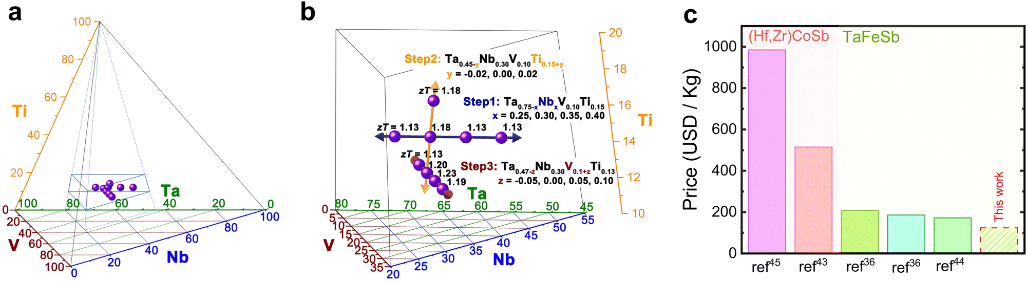 | ||
| Fig. 1 The step-wise optimization procedure of (Ta,Nb,V,Ti) FeSb-based half-Heusler compound. (a) The whole quaternary phase among Ta (green axis), Nb (blue), V (brown), and Ti (yellow). The purple spheres represent the investigated compositions in this work. (b) The enlarged view of the left. The zT values labelled at each composition are experimental results at 973 K, (c) price comparison between most promising p-type HHs36,43–45 and this study. | ||
2.2. Improving the thermoelectric performance through a composite strategy
In Fig. 2a, it is evident that σ increases with the addition of InSb. The enhancement is particularly prominent at room temperature, with a maximum increase of 20% observed for δ = 0.03. Notably, the InSb-containing sample (δ = 0.015) exhibit very good repeatability (Fig. S4, ESI†) and cyclability with repeated heating and cooling (Fig. S5, ESI†), even though the measurement temperature exceeds the melting point of InSb. Additionally, as Fig. S3c (ESI†) shows, the Ta0.42Nb0.3V0.15Ti0.13FeSb-(InSb)0.025 sample's XRD figure revealed InSb peaks after six times cycling and proved InSb phase's stability in the material. These results indicate an excellent thermal stability of our composites. Furthermore, as Fig. S6 (ESI†) and Fig. 2a (black dots) illustrate, the electrical conductivity of all specimens follows a power law with temperature (σ ∝ Tα) with index values, α of ∼−1 across the recorded temperatures. This α value differs from that of typical degenerate semiconductors, which usually takes α ∼ −1.5 because of the deformation-potential-induced lattice vibration scattering,46 as has been observed in typical degenerate semiconductors such as n-type Mg3Sb2 where the Hall concentration (nH) was optimized at ∼3 × 1019 cm−3.47 To understand the observed α ∼ −1, we performed Hall measurement for our specimens. Table 1 shows much higher nH values in this work that are located in the range of 2–3 × 1021 cm−3. As suggested by Ziman, greater screening can diminish the strength of scattering when the carrier concentration is raised, therefore reducing the temperature dependency to α ∼ −1.46 Furthermore, Table 1 suggested that adding InSb increases the Hall mobility (μH) by increasing δ until 0.015, then the μH decreases by further adding InSb. These results suggest a dual-role played by InSb in the mobility. This can be understood as like this: InSb itself is a semiconductor that exhibits high electron mobility of 7–8 m2 V−1 s−1 at room temperature. Its addition to a half-Heusler mixture can initially increase overall mobility by facilitating easier movement of carriers (Table 1). However, after 1.5% InSb, μH decreases, which likely stem from an enhanced secondary phase scattering and carrier-carrier scattering due to the increased nH.
 | ||
| Fig. 2 Electrical properties of Ta0.42Nb0.3V0.15Ti0.13FeSb-(InSb)δ (δ = 0, 0.015 and 0.03) half-Heuslers. (a) Temperature-dependent electrical conductivity and the power-law curve (black dotted plot). The pink color background shows distinctive “bumps” at temperatures higher than 750 K for specimens containing InSb, (b) temperature-dependent Seebeck coefficient, (c) weighted mobility versus temperature, (d) average power factor versus InSb content and power factor versus temperature. | ||
| δ | 0 | 0.01 | 0.015 | 0.02 | 0.025 | 0.03 |
|---|---|---|---|---|---|---|
| n H (1021 cm−3) | 2.16 | 2.20 | 2.22 | 2.34 | 2.41 | 2.71 |
| μ H (cm2 V−1 s−1) | 7.43 | 7.57 | 8.08 | 7.46 | 7.33 | 7.07 |
The Seebeck coefficient (S) of the material, as shown in Fig. 2b, exhibits a peculiar behavior with increasing InSb content. At room temperature, S rises from 118 μV K−1 to 127 μV K−1 as δ increases from 0 to 0.015 and degrades to 105 μV K−1 when δ increases to 0.03. Note that from δ = 0 to δ = 0.015, nH is nearly unchanged at ∼2.2 × 1021 cm−3, suggesting that In hardly functions as a dopant. In addition, by repeating the experiments, it is found that the S enhancement at δ = 0.015 is robust against batch variations, instead of due to measurement uncertainties (Fig. S7, ESI†). This non-monotonic trend in S has also been observed in other composite systems.23 For attaining deeper insights, we employ the Pisarenko relation to interrogate the impact of InSb on the Seebeck coefficient, where  . Herein,
  , kB and h signify the density-of-states (DOS) effective mass, Boltzmann constant and Planck constant respectively. Degenerate band extrema allow for an increase in
  ,
,  , where
  is the band effective mass (Fig. S8, ESI†).8 The Seebeck coefficient is increased and does not follow the usual inverse relationship with carrier concentration after addition of a small amount of InSb phase as shown in Fig. S8 (ESI†), which means the variation of S with InSb content is linked to the scattering parameter. The value of
  for the InSb-absent specimen is fitted as 9.5 me, whereas an increase to 10.5 me is observed with δ = 0.015. Conversely, upon reaching a δ value of 0.03, the Seebeck coefficient decreases and
  also decreases to 9 me. Variations in the effective mass of the density of states as shown by the Pisarenko plot fitting (Fig. S8, ESI†), point to a selective scattering process, suggesting that preferential scattering may occur for some charge carriers at certain energy levels, leading to changes in
  when trace amount InSb is added. However, more InSb addition increases nH, which will potentially shift the Fermi level away from the range where the selective-scattering effect is effective, resulting in a diminished effective mass. These observations align with the theoretical discussion that the nonmonotonic trend of the Seebeck coefficient relates an energy-dependent electronic scattering time when changing the concentration of the second phase.25 Furthermore, we adopted the weighted mobility concept48 as shown in Fig. 2c, the weighted mobility (μw) exhibited a consistent decrease with increasing temperature. Interestingly, the results highlighted that the introduction of modest amount of InSb (δ = 0.015) led to an increase in the μw, e.g., by 25% at 300 K, enabling a 23% enhancement of average PF (PFave) from 300 K to 973 K, as shown in Fig. 2d. Also note that analogous enhancements in power factor are also evident in samples featuring δ values of 0.01, 0.02, and 0.025, as shown in Fig. 2d and also in the ESI† (Fig. S9). The pronounced improvement in weighted mobility and power factor proves the efficacy of our composite approach, which has immense potential to enhance the electrical properties of more thermoelectrics.
The role of InSb in tuning electronic transport properties is complex and multifaceted. On one hand, the InSb phase enhances overall mobility by introducing a high-mobility secondary phase. On the other hand, it increases charge carrier scattering due to the presence of the secondary phase. These two mechanisms – high-mobility phase enhancement and selective scattering – are distinct yet interconnected, with diverse implications for thermoelectric optimization. Notably, both mechanisms may coexist synergistically, depending on the orientation of charge carrier transport relative to the grain boundaries. When charge carriers travel parallel to the InSb-modified grain boundaries, the high-mobility phase enhances mobility (Fig. S10a, ESI†). In contrast, perpendicular transport increases scattering due to a Kapitza-like effect (Fig. S10b, ESI†). In real conditions, electrons likely approach the grain boundaries at tilted angles (Fig. S10c, ESI†), striking a balance where parallel transport improves mobility while perpendicular scattering contributes to an enhanced Seebeck coefficient.
However, understanding the impact of InSb inclusion on transport properties remains challenging due to material complexity, including composition and carrier concentration. For example, in our previous study, InSb addition enhanced mobility in Nb0.95Ti0.05FeSb but did not improve the Seebeck coefficient.41 This discrepancy may arise from a chemistry-dependent mismatch in electronic properties, which affects the Kapitza resistance. Variations in chemistry shift relative energy levels in the band structure, altering the degree of mismatch and, consequently, the strength of the Kapitza effect. Comprehensive insights require further studies, such as interface ab initio calculations, high-resolution microscopy, transport property modeling, and atomic probe tomography, to unravel these mechanisms and guide future research.
To gain a deeper insight into the microstructures at the nanometer scale, we show in Fig. 3 EDX analysis conducted in a scanning transmission electron microscope (STEM). Fig. 3a contains a high-angle annular dark field (HAADF)-STEM image containing a GB, and the elemental mapping results are shown in Fig. 3b, which displays a clear enrichment of In and Sb at the GB, confirming our hypothesis. Additionally, we integrated the spectra to plot the composition profiles of different elements along the red arrow across the GB from the highlighted region in Fig. 3a. As shown in Fig. 3c, the line profiles give a quantitative view of the segregation and depletion of different elements across the GB. In addition to the enrichment of In and Sb, the depletion of matrix elements Ta, Nb, and Fe are observed. Moreover, note that the analysis showed an increase in Ti at the GB, whereas V hardly changes in composition across the GB. Indeed, Ti segregation at GBs has been observed in Nb0.8Ti0.2FeSb,40 participating in the formation of TiSb-like GB phases, which are found to be electrically conductive. Therefore, we can conclude that the GB phase in this material is enriched in (In,Ti)Sb. This result differs from the previous one of Nb0.95Ti0.05FeSb-InSb0.02 where the GB is rich only in In and Sb, suggesting that the changes of the chemical potentials can drive the GB modification in the compositions. Our findings provide insights into the role of GB modification in tailoring the transport properties and validate the microstructural foundation that is necessary for filtering low-energy carriers.
 | ||
| Fig. 3 HAADF-STEM image with EDX mapping of the GB of Ta0.42Nb0.3V0.15Ti0.13FeSb-(InSb)0.015. (a) HAADF-STEM image, (b) EDX maps from the area highlighted by the red box in (a) for In, Sb, Ta, Nb, Fe and Ti, (c) concentration line profiles of the elements across the GB. | ||
 | ||
| Fig. 4 Thermal transport properties and dimensionless fig of merit. (a) Temperature-dependent total thermal conductivity and electrical conductivity and, (b) temperature-dependent lattice thermal conductivity. The pink color background shows distinctive “bumps” at temperatures higher than 750 K for specimens containing InSb, (c) comparison of lattice thermal conductivity in RFeSb (R: Ta, Nb, and V) HHs8,34,36,37,41,55 (d) temperature dependent zT, and (e) zTaveversus InSb of Ta0.42Nb0.3V0.15Ti0.13FeSb-(InSb)δ, (f) comparison zT average among different p-type HHs8,36,38,43–45,55,58–60 and this study. | ||
The integration of InSb inclusions and alloying led to a remarkable synergistic enhancement in the power factor and the suppression of lattice thermal conductivity. Combined effect of these factors led to a significant improvement in the zT throughout the whole measured temperature range with a peak zT reaching 1.43 at 973 K (Fig. 4d). Moreover, for practical applications, the average zT (zTave) is more important than the peak value. As shown in Fig. 4e, increasing the parameter δ from 0 to 0.015 resulted in a significant 25% improvement in the zTave from 300 K to 973 K. By bringing the zTave to 1.0, this improvement represents an enhancement compared to the earlier p-type HHs (Fig. 4f).8,36,38,43–45,55,58–60 In addition, our strategy not only increased performance but also reduced production costs due to the efforts in reducing the Ta content, which is beneficial for the technology's applicability (Fig. 1c). This cost savings together with the increases in thermoelectric efficiency are in line with our objective of creating a lightweight, more affordable material and technology that may be used in real-world applications. The transport properties of our best composition, Ta0.42Nb0.3V0.15Ti0.13FeSb-(InSb)0.015, were further validated by measuring three individual samples and repeatedly measuring one specimen 6 times, and the thermoelectric properties are comparable (as shown in Fig. S4 and S5, ESI†). This shows that the high thermoelectric performance of the mentioned sample is stable and repeatable. This enhancement presents a promising avenue for the development of thermoelectric materials through selectively scattering lower-energy carriers via GB engineering.
3. Modules’ performance for power generation
We systematically measured both heat-to-electricity conversion efficiency (η) and output power (Pout) using a single-leg thermoelectric device within a custom-made system. The thermoelectric leg, featuring a cross-sectional area of 1.86![[thin space (1/6-em)]](https://www.rsc.org/images/entities/char_2009.gif) × 1.91 mm2 and a length of 11.236 mm, was positioned between a heater and a copper plate using mechanical force. To maintain the cold-side temperature, water circulation was employed, while PID control effectively regulated the hot-side temperature. Notably, these experiments were conducted in a high vacuum environment (below 10−6 mbar) to minimize heat conduction.
× 1.91 mm2 and a length of 11.236 mm, was positioned between a heater and a copper plate using mechanical force. To maintain the cold-side temperature, water circulation was employed, while PID control effectively regulated the hot-side temperature. Notably, these experiments were conducted in a high vacuum environment (below 10−6 mbar) to minimize heat conduction.
For the determination of conversion efficiency (η), concurrent measurements of output heat flow from the cold side (Qout) and generated power (P) were undertaken. Based on Fourier's law, a bulk polycrystalline copper, possessing known geometry and thermal conductivity, was positioned beneath the cold side to quantify heat flow (Qout). K-type thermocouples integrated at the interfaces facilitated the measurement of temperature differences in both the leg and copper bulk. It is pertinent to mention that the hot-side temperature of the copper served as the cold-side temperature of the leg. The calculation of η was performed using the 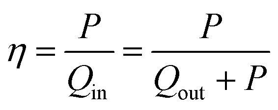 equation. Radiation heat loss was omitted as it is challenging to measure. Nevertheless, this treatment is deemed reasonable given that in practical thermoelectric modules, radiation loss can be minimized through proper engineering of module geometries and also applying advanced packing techniques, as partially investigated in our previous work.61 Through the adjustment of current in the circuit, we conducted a series of measurements for both Qout (output heat) and P (output power), enabling the determination of maximum η and P. The parameters for the single-leg Ta0.42Nb0.3V0.15Ti0.13FeSb-(InSb)0.015 were simultaneously acquired, including temperature difference, electric current (I), voltage (V), Pout, and Qin, as illustrated in Fig. 5a. Due to the limited heating power of the system, the hot-side temperature (Th) could only be elevated to approximately 823 K. The experimentally measured hot-side-temperature-dependent maximum output power density (ωmax) and maximum efficiency (ηmax) are presented in Fig. 5b and c. The peak efficiency reached around 8% at a hot-side temperature of approximately 823 K (Fig. 5c). It is essential to highlight that the obtained results exhibit a discrepancy with theoretical calculations, especially at high temperatures. This deviation is primarily attributed to parasitic electrical and heat losses. We anticipate that minimizing these adverse effects will bring the measured maximum efficiency and output power density closer to calculated values (approximately 12% and 3 W cm−2, respectively, at a hot-side temperature of around 823 K), as determined through simulations using the finite element method (FEM).
 | ||
| Fig. 5 Performance of a single-leg device based on the optimized material Ta0.42Nb0.3V0.15Ti0.13FeSb-(InSb)0.015. (a) Measured voltage, output power, input power, and efficiency with varying currents. The cold side and hot side of the device are fixed at ∼303 K and 823 K, respectively. Hot-side-temperature-dependent. (b) Maximum output power density (ωmax) and (c) maximum efficiency (ηmax). | ||
4. Conclusion
In summary, we successfully synthesized high-performing p-type TaFeSb-based half-Heusler materials with reduced Ta content while preserving high thermoelectric performance by alloying within the quaternary phase space among Ta, Nb, V, and Ti. Improved thermoelectric performances were obtained in an optimized composition, Ta0.42Nb0.3V0.15Ti0.13FeSb, where the peak zT reached 1.23 at 973 K and the zTave reached 0.8 between 300 K and 973 K. Furthermore, we applied a composite strategy by using InSb, yielding a subsequent gain of performances in composition Ta0.42Nb0.3V0.15Ti0.13FeSb-(InSb)0.015. A simultaneous improvement of the Seebeck coefficient and electrical conductivity, along with a further decrease in lattice thermal conductivity, resulted in a peak zT value of 1.43 at 973 K and a zTave of ∼1 between 300 K and 973 K. To the best of the authors' knowledge, the resultant zTave is the highest value among p-type half-Heusler compounds. Furthermore, we obtained a maximum conversion efficiency of around 8% at cold-side temperatures of 303 K and 823 K based on a single-leg device measurement. These findings highlight the exciting potential of our material design and production methods for not only this system but also shed light on the possibility of other materials systems for effective thermoelectric applications.5. Experimental
5.1. Materials preparation
Specimens of p-type RFeSb-(InSb)δ with nominal δ = 0, 0.01, 0.015, 0.02, 0.025, and 0.03 were prepared by mechanical alloying and sintering. In total 6 g of raw elements, including Ta powders (99.8%, Alfa Aesar), Nb powders (99.8%, Alfa Aesar), V powders (99.98%, Alfa Aesar), Fe granules (99.98%, Alfa Aesar), Ti sponges (99.95%, Alfa Aesar), In shot (99.9%, Alfa Aesar) and Sb pieces (99.999%, MaTecK) were weighted according to the stoichiometry in an Ar-filled glovebox with O2 and H2O levels lower than 1 ppm. Mechanical alloying was done for 25 hours by using a high-energy ball mill (SPEX 8000D), and the ball-milled powders were compacted to a disk by a field-assisted sintering technique (FAST, FCT Systeme GmbH) under a pressure of 50 MPa in vacuum for 3 min at 1123 K. Fast cold press before sintering process increases the density of the product and reducing the porosities. The densities of the sintered sample are determined by Archimedes's method, reaching 99% of the theorical densities.5.2. Characterization
The phase structure, morphology, grain size, and chemical composition of the specimens have been analyzed by X-ray diffraction (XRD), scanning electron microscopy (SEM), electron backscatter electron (EBSD) as well as scanning transmission electron scanning microscopy- energy-dispersive X-ray spectroscopy (STEM-EDX), respectively. Room temperature X-ray diffraction patterns of sintered bulk were measured by a Bruker D8 Advance diffractometer (Co Kα radiation) to characterize the phases. Thin samples for STEM experiments have been prepared using a Scios2 ThermoFisher focused ion beam following the procedure described by Schaffer et al.62 The specimen has been thinned down to <150 nm by 30 kV Ga+ beam and a final thinning has been performed at 5 and 2 kV. STEM experiments have been performed in a probe-corrected ThermoFisher Titan operated at 300 kV with a collection semiangle of 24 mrad and approx. <1 Å probe size. STEM-EDX maps were acquired using a four-quadrant silicon-drift EDX detector (Super-X) in approx. 30 min acquisition time for each map. Multivariate statistical analysis63 has been performed for noise reduction and the Cliff–Lorimer formula has been used for elemental quantification EBSD maps have been acquired according to Wilkinson et al.64 using a Sigma 500 SEM (ZEISS) operated at 15 kV and a Hikari EBSD camera. APEX software (EDAX) was used for acquisition and the OIM Analysis 8 software (EDAX) was used for analysis.5.3. Measurement
The sintered compounds were cut and polished into rectangular bar shapes for electrical conductivity and Seebeck coefficient measurements on a commercial device high-temperature LSR-3 (Linseis) system at the same time under an inert gas (He) atmosphere. The thermal conductivity (κ = DCpd) was calculated as a multiplication of thermal diffusivity (D) via the LFA-Linseis system, specific heat (Cp) (DSC 404, Netzsch), and mass density (d) (Archimedes’ kit). The measurement errors were 4%, 5%, and 12% for σ, S, and κ, respectively. Explicitly, the uncertainties of κ originated from 2% in mass density, 4% in diffusivity, and 6% in specific heat. Therefore, the nominal uncertainties in power factor and zT were 10% and 20%, respectively. The degree of uncertainty can be reduced upon reproducing the specimens, as implemented in this work. To increase the readability of the graphs, the error bars were not added to the curves. Hall carrier concentrations (nH) were taken on a quantum design physical properties measurement system (PPMS) with a magnetic field of ±9 T and an electric current of 8 mA at room T. Hall mobility (μH) was then calculated from μ = σ/nHe, were e is the elemental charge.5.4. Simulation and measurement for the single-leg device
COMSOL Multiphysics with heat transfer module is used to perform the three-dimensional finite-element simulations of the power-generation characteristics for the thermoelectric single leg. A geometrical model with the same dimensions as the experimental leg is used to calculate the electric power and heat flow outputs. The temperature-dependent Seebeck coefficient, electrical conductivity, and thermal conductivity for the material are taken from the measured data as material properties in the simulations. The efficiency of the single thermoelectric leg was assessed using a custom-built system. The leg, measuring 1.86 mm by 1.91 mm by 11.24 mm, was directly integrated into the setup for data collection, following the established double four-point probe method as detailed in a prior publication.65 The components – including the heater, single leg, heat meter, and heat sink – were aligned in series from top to bottom, with thermal grease applied to minimize thermal resistance. The entire measurement process was carried out under a vacuum of less than 10−6 bar. The heat meter situated beneath the thermoelectric leg was constructed from oxygen-free copper, featuring a cross-sectional area of 1.85 × 10⁻⁵ m2 and a length of 0.15 m. To mitigate potential errors arising from heat resistance and hysteresis at the interface, two thermocouples were strategically positioned at the center of the bar, spaced 0.01 m apart, to monitor thermal flow accurately.Author contributions
R. H. and Z. H. proposed the research. R. H. N. carried out the experiments and most thermoelectric measurements. R. B. V. D. A. M. and S. Z. performed SEM, EBSD, HAADF-STEM, and EDX experiments and gave their insight in the entire article. S. B. performed Hall measurement. P. Y. performed the simulation of the single-leg module. S. S. prepared and measured the module performance. K. N., C. S., and Z. R. commented on the results. R. H. N. and R. H. drafted the manuscript. R. H. N., R. H., S. Z., Z. H., and R. B. V. revised the manuscripts. All authors read and commented on the manuscript.Data availability
Data for this article, including the data files are available at Zenodo at [https://doi.org/10.5281/zenodo.13946591].Conflicts of interest
The authors declare no conflict of interest.Acknowledgements
This work is supported by Deutsche Forschungsgemeinschaft (DFG), Project Number 453261231. H. Z. acknowledges the financial support from the National Natural Science Foundation of China, Project Number 52172262, and the National Key Research and Development Program of China, Project Number 2022YFB3803900. C. S. and S. Z. acknowledge funding from the DFG within the Collaborative Research Centre SFB 1394 (Project ID 409476157). The authors acknowledge Birgit Bartusch for Cp measurement. R. H. N acknowledges the support from Prof. Jeff Snyder from Northwestern University and Ms Xin Ai from IFW for fruitful discussions.References
- W. Liu, Q. Jie, H. S. Kim and Z. Ren, Acta Mater., 2015, 87, 357–376 CrossRef CAS.
- B. Poudel, Q. Hao, Y. Ma, Y. Lan, A. Minnich, B. Yu, X. Yan, D. Wang, A. Muto, D. Vashaee, X. Chen, J. Liu, M. S. Dresselhaus, G. Chen and Z. Ren, Science, 2008, 320, 634–638 CrossRef CAS PubMed.
- G. J. Snyder and E. S. Toberer, Nat. Mater., 2008, 7, 105–114 CrossRef CAS PubMed.
- H. Tang, J. F. Dong, F. H. Sun, Asfandiyar, P. Shang and J. F. Li, Sci. China Mater., 2019, 62, 1005–1012 CrossRef CAS.
- J. Mao, Z. Liu, J. Zhou, H. Zhu, Q. Zhang, G. Chen and Z. Ren, Adv. Phys., 2018, 67, 69–147 CrossRef.
- Y. Liu, C. Fu, K. Xia, J. Yu, X. Zhao, H. Pan, C. Felser and T. Zhu, Adv. Mater., 2018, 30, e1800881 CrossRef PubMed.
- M. Zebarjadi, K. Esfarjani, M. S. Dresselhaus, Z. Ren and G. Chen, Energy Environ. Sci., 2012, 5, 5147–5162 RSC.
- R. He, D. Kraemer, J. Mao, L. Zeng, Q. Jie, Y. C. Lan, C. H. Li, J. Shuai, H. S. Kim, Y. Liu, D. Broido, C. W. Chu, G. Chen and Z. Ren, Proc. Natl. Acad. Sci. U. S. A., 2016, 113, 13576–13581 CrossRef CAS PubMed.
- T. Graf, C. Felser and S. S. P. Parkin, Prog. Solid State Chem., 2011, 39, 1–50 CrossRef CAS.
- S. Anand, K. Xia, I. V. Hegde, U. Aydemir, V. Kocevski, T. Zhu, C. Wolverton and G. J. Snyder, Energy Environ. Sci., 2018, 11, 1480–1488 RSC.
- S. Chen and Z. Ren, Mater. Today, 2013, 16, 387–395 CrossRef CAS.
- T. Zhu, C. Fu, H. Xie, Y. Liu and X. Zhao, Adv. Energy Mater., 2015, 5, 1500588 CrossRef.
- W. G. Zeier, J. Schmitt, G. Hautier, U. Aydemir, Z. M. Gibbs, C. Felser and G. J. Snyder, Nat. Rev. Mater., 2016, 1, 16032 CrossRef CAS.
- R. He, T. Zhu, P. Ying, J. Chen, L. Giebeler, U. Kühn, J. Grossman, Y. Wang and K. Nielsch, Small, 2021, 17, 2102045 CrossRef CAS.
- S. J. Poon, J. Phys. D: Appl. Phys., 2019, 52, 493001 CrossRef CAS.
- X. A. Yan, G. Joshi, W. S. Liu, Y. C. Lan, H. Wang, S. Lee, J. W. Simonson, S. J. Poon, T. M. Tritt, G. Chen and Z. Ren, Nano Lett., 2011, 11, 556–560 CrossRef CAS.
- G. Joshi, X. Yan, H. Wang, W. Liu, G. Chen and Z. Ren, Adv. Energy Mater., 2011, 1, 643–647 CrossRef CAS.
- R. J. Quinn and J. W. G. Bos, Mater. Adv., 2021, 2, 6244–6266 RSC.
- J. W. G. Bos and R. A. Downie, J. Phys.:Condens. Matter, 2014, 26, 433201 CrossRef.
- M. Schwall and B. Balke, Phys. Chem. Chem. Phys., 2013, 15, 1868–1872 RSC.
- R. A. Downie, D. A. MacLaren and J. W. G. Bos, J. Mater. Chem. A, 2014, 2, 6107 RSC.
- S. Populoh, M. H. Aguirre, O. C. Brunko, K. Galazka, Y. Lu and A. Weidenkaff, Scr. Mater., 2012, 66, 1073–1076 CrossRef CAS.
- W. J. Xie, Y. G. Yan, S. Zhu, M. Zhou, S. Populoh, K. Galazka, S. J. Poon, A. Weidenkaff, J. He, X. F. Tang and T. M. Tritt, Acta Mater., 2013, 61, 2087–2094 CrossRef CAS.
- L. I. Bytenskii, T. S. Gudkin, E. K. Iordanishvili, S. A. Kazmin, V. I. Kaidanov, S. A. Nemov and Y. I. Ravich, Sov. Phys. Semicond., 1977, 11, 894–896 Search PubMed.
- S. V. Faleev and F. Léonard, Phys. Rev. B:Condens. Matter Mater. Phys., 2008, 77, 214304 CrossRef.
- J. P. Heremans, C. M. Thrush and D. T. Morelli, J. Appl. Phys., 2005, 98, 063703 CrossRef.
- R. He, H. Zhu and S. Chen, in Novel thermoelectric materials and device design concepts, ed. S. Skipidarov and M. Nikitin, Springer, 2019 Search PubMed.
- X. Ai, B. Lei, M. O. Cichocka, L. Giebeler, R. Bueno Villoro, S. Zhang, C. Scheu, N. Pérez, Q. Zhang, A. Sotnikov, D. J. Singh, K. Nielsch and R. He, Adv. Funct. Mater., 2023, 33, 2305582 CrossRef CAS.
- L. Abdellaoui, Z. Chen, Y. Yu, T. Luo, R. Hanus, T. Schwarz, R. Bueno Villoro, O. Cojocaru-Mirédin, G. J. Snyder, D. Raabe, Y. Pei, C. Scheu and S. Zhang, Adv. Funct. Mater., 2021, 31, 2101214 CrossRef CAS.
- L. Abdellaoui, S. Zhang, S. Zaefferer, R. Bueno-Villoro, A. Baranovskiy, O. Cojocaru-Mirédin, Y. Yu, Y. Amouyal, D. Raabe, G. J. Snyder and C. Scheu, Acta Mater., 2019, 178, 135–145 CrossRef CAS.
- A. Page, A. Van der Ven, P. F. P. Poudeu and C. Uher, J. Mater. Chem. A, 2016, 4, 13949–13956 RSC.
- Y. Kimura and Y. W. Chai, JOM, 2015, 67, 233–245 CrossRef CAS.
- C. G. Fu, T. J. Zhu, Y. Z. Pei, H. H. Xie, H. Wang, G. J. Snyder, Y. Liu, Y. T. Liu and X. B. Zhao, Adv. Energy Mater., 2014, 4, 1400600 CrossRef.
- C. G. Fu, T. J. Zhu, Y. T. Liu, H. H. Xie and X. B. Zhao, Energy Environ. Sci., 2015, 8, 216–220 RSC.
- R. He, H. Zhu, J. Sun, J. Mao, H. Reith, S. Chen, G. Schierning, K. Nielsch and Z. Ren, Mater. Today Phys., 2017, 1, 24–30 CrossRef.
- H. Zhu, J. Mao, Y. W. Li, J. F. Sun, Y. M. Wang, Q. Zhu, G. N. Li, Q. C. Song, J. W. Zhou, Y. H. Fu, R. He, T. Tong, Z. H. Liu, W. Y. Ren, L. You, Z. M. Wang, J. Luo, A. Sotnikov, J. M. Bao, K. Nielsch, G. Chen, D. J. Singh and Z. Ren, Nat. Commun., 2019, 10, 270 CrossRef.
- J. Yu, C. Fu, Y. Liu, K. Xia, U. Aydemir, T. C. Chasapis, G. J. Snyder, X. Zhao and T. Zhu, Adv. Energy Mater., 2018, 8, 1701313 CrossRef.
- H. Zhu, W. Li, A. Nozariasbmarz, N. Liu, Y. Zhang, S. Priya and B. Poudel, Nat. Commun., 2023, 14, 3300 CrossRef CAS PubMed.
- T. Luo, F. Serrano-Sánchez, H. Bishara, S. Zhang, R. Bueno Villoro, J. J. Kuo, C. Felser, C. Scheu, G. J. Snyder, J. P. Best, G. Dehm, Y. Yu, D. Raabe, C. Fu and B. Gault, Acta Mater., 2021, 217, 117147 CrossRef CAS.
- R. Bueno Villoro, D. Zavanelli, C. Jung, D. A. Mattlat, R. Hatami Naderloo, N. Pérez, K. Nielsch, G. J. Snyder, C. Scheu, R. He and S. Zhang, Adv. Energy Mater., 2023, 13, 2204321 CrossRef CAS.
- R. Bueno Villoro, R. Hatami Naderloo, D. A. Mattlat, C. Jung, K. Nielsch, C. Scheu, R. He and S. Zhang, Mater. Today Phys., 2023, 38, 101240 CrossRef CAS.
- Z. L. Du, J. He, X. L. Chen, M. Y. Yan, J. H. Zhu and Y. M. Liu, Intermetallics, 2019, 112, 106528 CrossRef CAS.
- N. S. Chauhan, S. Bathula, A. Vishwakarma, R. Bhardwaj, K. K. Johari, B. Gahtori and A. Dhar, J. Mater., 2019, 5, 94–102 Search PubMed.
- P. Luo, C. Lin, Z. Li, J. Zhang and J. Luo, ACS Appl. Energy Mater., 2023, 6, 10070–10077 CrossRef CAS.
- R. He, H. S. Kim, Y. Lan, D. Wang, S. Chen and Z. Ren, RSC Adv., 2014, 4, 64711–64716 RSC.
- J. M. Ziman and A. H. Kahn, The theory of transport phenomena in solids, Oxford University Press, 1961 Search PubMed.
- K. Imasato, C. Fu, Y. Pan, M. Wood, J. J. Kuo, C. Felser and G. J. Snyder, Adv. Mater., 2020, 32, 1908218 CrossRef CAS.
- G. J. Snyder, A. H. Snyder, M. Wood, R. Gurunathan, B. H. Snyder and C. Niu, Adv. Mater., 2020, 32, 2001537 CrossRef CAS PubMed.
- S. Zhu, Doctor of Philosophy Physics's thesis, Clemson University, 2013.
- K. F. Hulme and J. B. Mullin, Solid-State Electron., 1962, 5, 211–IN210 CrossRef CAS.
- C. Gayner and Y. Amouyal, Adv. Funct. Mater., 2020, 30, 1901789 CrossRef CAS.
- R. Bueno Villoro, M. Wood, T. Luo, H. Bishara, L. Abdellaoui, D. Zavanelli, B. Gault, G. J. Snyder, C. Scheu and S. Zhang, Acta Mater., 2023, 249, 118816 CrossRef CAS.
- Z. Ren, Y. Lan and Q. Zhang, Advanced thermoelectrics: materials, contacts, devices, and systems, CRC Press, 2018 Search PubMed.
- H. S. Kim, Z. M. Gibbs, Y. Tang, H. Wang and G. J. Snyder, APL Mater., 2015, 3, 041506 CrossRef.
- S. Ghosh, A. Nozariasbmarz, H. Lee, L. Raman, S. Sharma, R. B. Smriti, D. Mandal, Y. Zhang, S. K. Karan, N. Liu, J. L. Gray, M. Sanghadasa, Y. Xia, S. Priya, W. Li and B. Poudel, Joule, 2024, 8, 1–10 CrossRef.
- B. Abeles, Phys. Rev., 1963, 131, 1906–1911 CrossRef.
- S. Han, S. Dai, J. Ma, Q. Ren, C. Hu, Z. Gao, M. Duc Le, D. Sheptyakov, P. Miao and S. Torii, Nat. Phys., 2023, 19, 1649–1657 Search PubMed.
- H. Zhu, R. He, J. Mao, Q. Zhu, C. Li, J. Sun, W. Ren, Y. Wang, Z. Liu, Z. Tang, A. Sotnikov, Z. Wang, D. Broido, D. J. Singh, G. Chen, K. Nielsch and Z. Ren, Nat. Commun., 2018, 9, 2497 Search PubMed.
- X. Bao, K. Liu, X. Ma, X. Li, H. Yao, S. Ye, F. Cao, J. Mao and Q. Zhang, ACS Appl. Mater. Interfaces, 2024, 16, 3502–3508 CrossRef CAS.
- C. Fu, S. Bai, Y. Liu, Y. Tang, L. Chen, X. Zhao and T. Zhu, Nat. Commun., 2015, 6, 8144 CrossRef.
- P. Ying, H. Reith, K. Nielsch and R. He, Small, 2022, 18, 2201183 CrossRef CAS.
- M. Schaffer, B. Schaffer and Q. Ramasse, Ultramicroscopy, 2012, 114, 62–71 CrossRef CAS PubMed.
- S. Zhang and C. Scheu, Microscopy, 2017, 67, i133–i141 CrossRef.
- A. J. Wilkinson and T. B. Britton, Mater. Today, 2012, 15, 366–376 CrossRef CAS.
- Q. Zhu and Z. Ren, Energy, 2020, 191, 116599 CrossRef CAS.
Footnote |
| † Electronic supplementary information (ESI) available. See DOI: https://doi.org/10.1039/d4ee04819a |
| This journal is © The Royal Society of Chemistry 2025 |