
 Open Access Article
 This Open Access Article is licensed under a Creative Commons Attribution-Non Commercial 3.0 Unported Licence
Opportunities and challenges for emerging inorganic chalcogenide–silicon tandem solar cells†
Vijay C.
Karade
 ab,
Mingrui
He
c,
Zhaoning
Song
a,
Abasi
Abudulimu
a,
Yeonwoo
Park
b,
Donghoon
Song
de,
Yanfa
Yan
a,
Jin Hyeok
Kim
f,
Randy J.
Ellingson
a,
Jae Ho
Yun
*b,
Xiaojing
Hao
c,
Seung Wook
Shin
*g and
Mahesh P.
Suryawanshi
*c
ab,
Mingrui
He
c,
Zhaoning
Song
a,
Abasi
Abudulimu
a,
Yeonwoo
Park
b,
Donghoon
Song
de,
Yanfa
Yan
a,
Jin Hyeok
Kim
f,
Randy J.
Ellingson
a,
Jae Ho
Yun
*b,
Xiaojing
Hao
c,
Seung Wook
Shin
*g and
Mahesh P.
Suryawanshi
*c
aDepartment of Physics and Astronomy and Wright Center for Photovoltaics Innovation and Commercialization, The University of Toledo, 2801 W. Bancroft Street, Toledo, OH 43606, USA
bDepartment of Energy Engineering, Korea Institute of Energy Technology (KENTECH), Naju 522132, Republic of Korea. E-mail: jhyun@kentech.ac.kr
cSchool of Photovoltaic and Renewable Energy Engineering, University of New South Wales, Sydney, New South Wales 2052, Australia. E-mail: m.suryawanshi@unsw.edu.au
dDepartment of Chemical Engineering, Sunchon National University, Suncheon 57922, Republic of Korea
eSchool of Materials Science and Engineering, Georgia Institute of Technology, North Ave NW, Atlanta, Georgia 30332, USA
fOptoelectronics Convergence Research Center and Department of Materials Science and Engineering, Chonnam National University, Gwangju 61186, Republic of Korea
gFuture Agricultural Research Division, Rural Research Institute, Korea Rural Community Corporation, Ansan-si 15634, Republic of Korea. E-mail: swshin1211@gmail.com
First published on 2nd May 2025
Abstract
This review highlights the promise of emerging inorganic chalcogenide–silicon (Si) tandem solar cells (TSCs) to overcome the power conversion efficiency (PCE) and long-term stability limitations of single-junction solar cells, advancing them toward early commercialization. First, we cover the fundamentals of TSCs, including basic concepts, design considerations, and key requirements. The unique optoelectronic properties of proven and emerging chalcogenide absorber materials are then thoroughly examined to evaluate whether they are suitable candidates for the top cell in tandem configurations. Furthermore, we highlight the critical factors that limit PCE when compared to III–V-, Si-, and perovskite-based tandem and single-junction solar cells. In light of limitations, we discuss the challenges and solutions for the fabrication process, device performance, long-term stability, and outdoor testing of chalcogenide–Si TSCs. Finally, we provide perspectives on future research directions and potential pathways for the early commercialization of these emerging inorganic chalcogenide–Si tandem technologies.
 Vijay C. Karade | Dr Vijay C. Karade is currently a postdoctoral researcher at the University of Toledo, affiliated with the Department of Physics and Astronomy and PVIC. His research focuses on chalcogenide-based thin-film photovoltaics and tandem solar cells. He earned his Ph.D. in Materials Science and Engineering from Chonnam National University, South Korea, specializing in kesterite-based solar cells, and later pursued postdoctoral research at KENTECH on CIGS-perovskite tandem cells. With expertise in thin-film deposition, device fabrication, and performance optimization, he works to advance next-generation solar technologies. |
 Jae Ho Yun | Prof. Jae Ho Yun is currently a professor in the Department of Energy Engineering at KENTECH, South Korea. Previously, he served as the director of the PV division at the Korea Institute of Energy Research (KIER), where he pioneered solar cells, modules, and system technologies. During his tenure, he developed world-class flexible thin-film solar cells and successfully transferred them to industry. He has founded multiple research-based spin-off companies and currently focuses on high-efficiency flexible tandem solar cells and next-generation photovoltaic systems for distributed renewable energy. His work advances carbon neutrality and sustainable energy solutions. |
 Seung Wook Shin | Dr Seung Wook Shin is a senior researcher professor at the Rural Research Institute, Korea Rural Community Corporation. His work focuses on the synthesis and characterization of inorganic energy conversion materials and their applications, including thin-film solar cells and photoelectrochemical water-splitting devices. |
 Mahesh P. Suryawanshi | Dr Mahesh P. Suryawanshi is an ARC DECRA Fellow and lecturer at the School of Photovoltaic and Renewable Energy Engineering, UNSW Sydney. He has received multiple prestigious awards, including a Doctoral Exchange Scholarship (2012), the Brain-Korea (BK-21) Postdoctoral Fellowship (2016–2019), the Early Career Researcher Award (2019–2021) from Ministry of Spain and the European Commission, and the Australian Research Council's Discovery Early Career Researcher Award (DECRA) (2021–2024). Since 2021, he leads a research group that focuses on the nanoscale design and development of functional materials, exploring their structure-optoelectronic properties through experiments and modeling for solar energy conversion and catalysis applications. |
Broader contextPhotovoltaics (PV) offers a promising solution to the challenges of replacing traditional fossil fuel with renewable energy and increasing energy demands in the near future. Although various single-junction PVs (i.e., Si) are widely installed in the world, their power conversion efficiency (PCE) faces the theoretical limitation. In this regard, tandem solar cells (TSCs) are attractive for new pathways to overcome these limitations. Unfortunately, the well developed III–V-Si and perovskite-Si TSCs have critical issues such as elemental scarcity, high costs, instability in an air atmosphere, and toxicity despite their high PCE. On the other hand, emerging inorganic metal–chalcogenide materials have excellent advantages as the top cell in TSCs, including cost-effectiveness, non- or lower-toxicity, tunable and excellent optoelectronic properties, and long-term stability in an air atmosphere. However, few investigations of emerging inorganic metal chalcogenide-Si TSCs have been reported. This review addresses a significant gap in the literature by providing a comprehensive overview of the advancements, potential, and challenges of using emerging inorganic chalcogenide materials as a top cell in Si-based tandem solar cells. |
1. Introduction
The growing global demand for renewable energy necessitates continuous advancements in solar cell (SC) technologies and the photovoltaic (PV) market. Over the years, significant progress has been made in highly efficient single-junction SCs (e.g., silicon (Si), CdTe, and Cu(In,Ga)Se2 (CIGSe)), enabling them to convert sunlight into useful energy more effectively.1,2 However, these conventional single-junction SCs, have a theoretical maximum power conversion efficiency (PCE) limit of around 33.7% for a band gap energy (Eg) of 1.34 eV.3 To overcome this limitation, “tandem SCs (TSCs)” have emerged as a promising solution, utilizing multiple absorber layers, each optimized for a specific range of the solar spectrum.4,5 In tandem configurations, the top cell has a wider Eg, with each subsequent cell having a progressively narrower Eg,6 enabling the better utilization of sunlight and hence higher PCE. In this regard, TSCs offer the potential to overcome the PCE limits of single-junction SCs and drive solar energy technology to new heights.7Currently, commercialized III–V-based TSCs (GaAs-based compounds) have excellent PCEs of 47.1%.8 However, their high costs and complex manufacturing processes prevent scale production.9 In this context, perovskite (PSK)-based TSCs, such as PSK-Si, PSK-inorganic (i.e., CIGSe or CdTe), and PSK–PSK, are attracting attention because of their high PCE, low cost, process compatibility, and tunable Eg.10–15 To date, the highest reported PCE for two-terminal (2T) and four-terminal (4T) PSK-CIGSe TSCs are approximately 24.616 and 29.9%,17 respectively. In contrast, PSK-Si TSCs have achieved much higher PCEs of 34.6% (2T) and 30.35% (4T).18–20 This demonstrates that Si is the most suitable bottom absorber material due to its low cost, reliability (minimum 80% warranty with initial peak performance lasting up to 30–35 years), and well-established commercial fabrication process.21–24 However, there are substantial concerns about the long-term stability and reliability of PSK-Si-based TSCs, notably light-induced phase segregation in bromine (Br)-rich PSKs.25,26 More critically, the high PCE PSK SCs contain lead (Pb), which severely limits their future commercialization. Despite several attempts to address this issue, effective strategies remain inadequate. Exploring alternative materials and strategies is crucial for overcoming these constraints and realizing the full potential of TSCs.
The inorganic chalcogenide absorber materials offer intrinsic long-term stability and durability, making them attractive candidates for top cells in Si-based TSC development.27,28 These materials have excellent optoelectronic properties, tunable Eg, and high thermal, chemical, and environmental stability, making them suitable for long-term solar energy harvesting applications (Fig. 1(a)).27–30 CIGSe and CdTe single-junction SCs with Eg (1.1–1.5 eV) have achieved PCEs of over 23% and are commercially available.19,31 However, the scarcity of indium (In), gallium (Ga), and tellurium (Te), as well as the toxicity of cadmium (Cd) necessitates the development of new chalcogenide-based absorber materials that use low-cost, less toxic, and earth-abundant elements.28,29,32 Integrating these emerging absorber materials with Si SCs offers promising solutions to the limitations of current TSC configurations. To produce high PCE TSCs, the top cell should have an Eg of 1.6–2.0 eV with PCE of >16% to exceed the 25% PCE mark of single junction Si SCs.33 However, the current highest PCEs reported for emerging inorganic wide Eg SCs such as Cu(In,Ga)S2 (CIGS) and CuGaSe (CGSe) are 16.9 and 11.9%,34 respectively, which fall short of the requirements, whilst others have achieved PCEs of 10% or lower.28,29,31,35 Despite promising results, there have been few research articles and reviews on inorganic chalcogenide–Si TSCs published.
 | ||
| Fig. 1 (a) Schematic of a TSC consisting of emerging chalcogenide-based wide Eg absorber layer as top cell and narrow Eg bottom cell (i.e., Si), (b) spectral irradiance under AM 1.5G for narrow Eg top cell and Si bottom cell for tandem configuration and (c) schematic of connection in 2T and 4T chalcogenide top cell-Si device structure. | ||
This comprehensive review highlights the current state of the art in emerging inorganic chalcogenide–Si TSCs, with a focus on fabrication, high PCE, and long-term stability challenges. We highlight advancements and challenges in III–V, PSK, CIGSe, and Si-based TSCs, as well as the optoelectronic properties of proven and emerging chalcogenide absorber materials. Moreover, we discuss current achievements, challenges, and opportunities for chalcogenide–Si TSCs. Finally, we provide perspectives and further research directions for the early commercialization of these promising emerging inorganic chalcogenide–Si TSCs technologies.
2. Principles of TSCs
The tandem concept is designed on the principle of maximum utilization of light, where the carrier losses caused by the thermalization process and absorption loss below the Eg can be minimized.36,37 Briefly, it can be achieved by integrating or stacking two or more absorber layers on top of each other with different Eg values, typically wider at the top and narrower at the bottom (Fig. 1(b)). In the case of chalcogenide–Si TSCs, the wide Eg chalcogenide absorber layer can absorb high-energy photons (typically ultraviolet visible (UV) region) from the solar spectrum, while transmitting low-energy photons (i.e., visible-infrared) efficiently harvested by the Si bottom cell (Fig. 1(b)). Generally, TSC configurations are categorized based on terminal configuration and integration techniques, such as 2T and 4T.7 In 2T configuration, the top cell is directly fabricated over the bottom cell, which allows a direct series connection of two sub-cells, whereas in 4T top cell is fabricated independently and stacked over the bottom cell (Fig. 1(c)). They are optically coupled but are electrically isolated. In 2T TSCs, the current matching is required as the same current flows through the two sub-cells connected in series, while in 4T it is not required as they are electrically isolated. Theoretically, both 2T and 4T Si-based TSCs with an Eg of 1.1–1.2 eV can achieve PCEs > 45%.38For a sustainable future, TSCs must exhibit commercial viability, scalability, ease of processing, low cost, and use earth-abundant and non-toxic elements.2,39 They must be robust against environmental conditions such as temperature and humidity, ensuring long-term performance stability. Moreover, while fabricating the TSC devices, interconnecting techniques, optical design, Eg, stacking orders, and fabrication process must be seriously considered.7,40 Particularly, there must be a suitable recombination layer (RL) to enable efficient charge transport between the monolithically integrated top and bottom cells, while maintaining light management features like anti-reflection (AR), surface texturing, and plasmonics.41,42 Choosing a suitable Eg and device configuration allows for the realization of maximum tandem efficiency.6,37 The low defect density in the top absorber layer is also crucial, along with achieving maximum current density and voltage (J–V) output through proper serial electrical interconnection between the two cells.43 Additional details on Eg selection, current matching criteria, and the foundation of TSCs can be found in earlier reports,5–7,44 and a detailed discussion concerning chalcogenide top cells can be found in Section 5.
3. Promising chalcogenide absorber materials
This section reviews the unique optoelectronic properties and recent progress of single-junction SCs in proven wide Eg chalcogenides, including CIGS, CGSe, CuInS2, Cu2ZnSn(S,Se)4 (CZTSSe), and Sb2(S,Se)3. Additionally, it covers emerging inorganic chalcogenide compounds such as SnS, GeSe, AgBiS2, CuBi(S,Se)2, BaZrS3, SrZrS3, and Ba3ZrS7. A summary of their optoelectrical properties and device parameters is provided in Tables 1 and 2.| Materials | Crystal structure | E g (eV) | α (cm−1) | N A (cm−3) | τ (ns) | μ h (cm2 V−1 s−1) | σ h (S cm−1) |
|---|---|---|---|---|---|---|---|
| CIGS(e)45,46 | Chalcopyrite | 1.0–1.7** | 104–105 | 1014–1018 | 20–50 | 10–100 | 1–10−2 |
| CZTS(e)47 | Kesterite | 1.0–1.5** | 104–105 | 1014–1018 | 5–10 | 7 | 10−2–10−3 |
| Sb2S(e)348 | Orthorhombic | 1.0–1.7* | 104–105 | 1017–1019 | — | 10–42 | 10−5–10−7 |
| GeS(e)49 | Orthorhombic | 1.14–1.7* | 104–105 | 1017–1019 | — | 128 | 1–10−7 |
| SnS50,51 | Orthorhombic | 1.1** | 104–106 | 1013–1015 | — | 10–15 | 10−3–10−1 |
| AgBiS252,53 | Hexagonal Cubic | 1.07* | 105–107 | 1014–1019 | — | 0.07–1.1 | 0.2–1 |
| 0.8** | |||||||
| NaBiS254 | Hexagonal Cubic | 1.2–1.5* | 103–104 | 1014–1019 | — | 0.03–0.29 | 10−6–10−5 |
| BaZrS355,56 | Hexagonal Cubic | 1.3–2.2* | 104–106 | 1017–1020 | — | 30–40 | 2.9 |
| Absorber | E g (eV) | V oc (mV) | J sc (mA cm−2) | FF (%) | PCE (%) |
|---|---|---|---|---|---|
| AgBiS2 | 1.30 | 518 | 27.2 | 72.4 | 10.2 |
| AgBiS2 | 1.39 | 495 | 27.1 | 68.4 | 9.2 |
| CGSe | 1.62 | 1017 | 17.5 | 67.0 | 11.934 |
| CIGS | 1.60 | 954 | 24.8 | 71.5 | 16.9 |
| CIS | 1.60 | 729 | 21.8 | 71.7 | 11.4 |
| CZGS | 1.45 | 625 | 24.4 | 55.7 | 8.5 |
| CZTS | 1.55 | 749 | 23.4 | 68.9 | 13.2 |
| CZTSSe | 1.09 | 530 | 38.4 | 74.0 | 15.1 |
| CZTSSe-Ag | 1.10 | 565 | 35.4 | 70.3 | 14.1 |
| CZTSSe-Ge | 1.12 | 527 | 32.3 | 72.3 | 12.3 |
| GeS | 1.70 | 530 | 8.30 | 31.0 | 1.3 |
| SnS | 1.25 | 339 | 25.8 | 55.0 | 4.860 |
| Sb2(S,Se)3 | 1.35 | 551 | 26.0 | 70.1 | 10.1 |
| Sb2(S,Se)3 | 1.44 | 631 | 25.3 | 67.4 | 10.8 |
| Sb2(S,Se)3 | 1.54 | 673 | 23.7 | 66.8 | 10.7 |
| Sb2S3 | 1.73 | 757 | 17.4 | 60.5 | 8.0 |
| Sb2S3 | 1.80 | 711 | 16.1 | 65.0 | 7.5 |
| Sb2Se3 | 1.23 | 467 | 33.5 | 67.6 | 10.6 |
| Sb2Se3 | 1.38 | 474 | 27.7 | 62.2 | 8.1 |
| c-Si | 1.11 | 745 | 42.3 | 86.7 | 27.4 |
| GaAs | 1.42 | 1127 | 29.8 | 86.7 | 29.1 |
| Perovskite | 1.53 | 1193 | 26.5 | 84.5 | 26.7 |
| CdTe | — | 904 | 31.6 | 80.6 | 23.1 |
| CIGSe | 1.13 | 767 | 38.3 | 80.5 | 23.6 |
3.1. Proven shalcogenides
 | ||
| Fig. 2 Atomic crystal structures for the different chalcogenide-based absorber layers, (a) Sb2S3 (Pnma), (b) CuInS2, (c) Cu2ZnSnS4, (d) SnS/GeS (Pnma), (e) AgBiS2 (P3m1), (f) AgBiS2 (F3m1), (g) BaZrS3, and (h) SbSI chalcohalaide, respectively. All crystal structures were created with VESTA software based on crystallographic information file from the inorganic crystal structure database (ICSD). | ||
3.2. Emerging chalcogenides
Another promising material in this class is NaBiS2, which comprises earth-abundant, cost-effective, and non-toxic elements. NaBiS2 exhibits a high absorption coefficient exceeding 105 cm−1 at and beyond its pseudo-direct Eg of 1.4 eV.54,115–117 This leads to a calculated spectroscopic limited maximum efficiency of 26% under 1 Sun illumination conditions.118 NaBiS2 shares a cation-disordered phase (space group: Fm3m) similar to AgBiS2,119 where Na+ and Bi3+ cations can randomly occupy the same crystallographic lattice site due to their similar ionic radii. It has been shown that free electrons and holes generated after photoexcitation could be localized to varying degrees at Bi3+- and Na+-rich clusters, respectively.118,120 Na+ clusters induce S-3p states just above the valence band maximum (VBM), leading to strong hole localization and the formation of small polarons. Consequently, the sum mobility of NaBiS2 nanocrystal films significantly decreases from 0.29 to 0.03 cm2 V−1 s−1 within 1 ps after photoexcitation.98 These favorable optoelectronic properties of NaBiS2 stem from its high density of states (DOS) in the upper VB and the pseudo-direct nature of the Eg. However, the spectator character of Na+ also results in the formation of localized s–p states above the VBM, particularly at Na+-rich clusters due to an inhomogeneous cation distribution.98 These localized states cause strong hole self-trapping, resulting in a slow relaxation process lasting several microseconds, unaffected by post-annealing treatment. Despite the reduction in sum mobility by almost an order of magnitude within a few picoseconds due to charge-carrier localization, the strong absorption and long-lived photogenerated charge carriers suggest the potential use of NaBiS2 in ultrathin single-junction SCs and possibly as top cell absorber materials in Si TSCs.
Chalcogenide PSKs also exhibit remarkable light absorption. Their band edges, dominated by sulfur 3p valence and transition metal d conduction states, result in a high joint DOS,56,124 leading to a rapid absorption coefficient rise (>105 cm−1) within 0.3–0.5 eV above the onset.130,131 Comparison with established PV materials shows absorption coefficients up to an order of magnitude higher.132,133 While charge transport studies remain limited, computational results suggest low effective masses for electrons and holes due to dispersive band edges.131 Experimentally, electron and hole mobilities of 13.7 and 9.4 cm2 V−1 s−1, respectively, are comparable to other direct Eg inorganic semiconductors,133–136 indicating their potential for TFSCs, including single-junction and Si-tandem configurations.
Additionally, V–VI–VII pnictogen chalcohalides such as SbSI and BiSI have been investigated for optoelectronic applications.141 These materials crystallize in an orthorhombic Pnma space group, forming a 1D ribbon-like structure along the c-axis (Fig. 2(h)). Covalent bonding along the ribbons and weak van der Waals interactions between them yield electronic and carrier transport properties comparable to binary Sb2S3.141,142 BiSY- and SbSY-based chalcohalides exhibit theoretically predicted Eg values of 1.6–1.87 eV and 2.1–2.3 eV, with experimental values of 1.9 and 2.1 eV, except for the iodide variant.138,140,143,144 SbSI demonstrates high carrier mobility ranging from 50–100 V−1 s−1 and electrical conductivity 10−7 Ω−1 cm−1.145,146 These properties, along with their tunable compositions and structural diversity, position chalcohalides as promising candidates for next-generation optoelectronic and PV applications, including single-junction and tandem SCs.
4. Opportunities and challenges
4.1. Silicon as suitable bottom cells
Si SCs stand as a mature, commercially developed PV technology, and with crystalline Si (c-Si) it dominates the PV market with a substantial share.147 Homojunction SCs (HJS), Si heterojunction SCs (SHJ), and c-Si based tandems are gaining market momentum, according to the latest report by the International Technology Roadmap for Photovoltaics (ITRPV) (Fig. 3).148 Recently, LONGi has set a new world record with 27.3% for heterojunction back contact cells and 22.7% for passivation emitter rear contact (PERC) modules.149,150 It shows PCE of single-junction Si SCs is approaching the theoretical limit of ∼29.4% along with growing production.151 Despite facing challenges in module PCE and capital expenditure, Si remains a preferred TSC material choice due to its long-term operational stability, developed and scalable processing techniques, the second most abundant element in the Earth's crust, and non-toxicity.152 Though, some inherent limitations come from spectral losses due to the inability to absorb infrared photons with energy < Eg and thermalization losses of high energy photons, restraining their PCE.153 The successful integration of Si with wide Eg materials as a top cell offers an opportunity for efficient light harvesting and exceptional performance. | ||
| Fig. 3 Predicted market capture of different c-Si SCs technologies based on the annual report produced by the International Technology Roadmap for Photovoltaics (ITRPV).148 Reproduced with permission, Copyright 2023, Cell press. | ||
The present section gives a brief overview of technological development in Si-based single-junction SCs. Based on device technology it can be classified into diffusion-based HJS and SHJ. An HJS includes Al back surface field (Al-BSF) cells, PERC, Tunnel Oxide Passivated Contact (TOPCon) and integrated back contact (IBC) as shown in Fig. 4.
 | ||
| Fig. 4 Different c-Si SCs architectures for Al-BSF, PERC, TOPCon, SHJ and IBC. | ||
4.2. Tandem configuration and best Si bottom cell selection
In terms of device stacking, the typical chalcogenide absorber layers can be fabricated in both n–p and p–n device configurations, defined by the fabrication sequence of the semiconductor thin films, (i.e., whether the n-type emitter is deposited before or after the p-type chalcogenide absorber). Materials such as Sb2S3, GeS, and AgBiS2 have demonstrated higher PCE in the supertartrate (n–p) configuration, while materials like CXTS, CTS, and CGS have shown better performance in the substrate (p–n) configuration. Therefore, similar to PSK-Si TSCs, one should be cautious while deciding on the absorber polarity, Si polarity, and p–n junction location.159,160 In the bottom Si SCs, the choice of Si wafer type mainly determines the junction location (p-type wafer: front junction and n-type wafer: rear junction) and studies in PSK-Si TSCs have shown that this switching of junction location can affect the overall tandem PCE.160,161 Materials like Sb2S3, chalcogenide PSK, and AgBiS2 sometimes utilize 2,2′,7,7′-tetrakis[N,N-di(4-methoxyphenyl)amino]-9,9′-spirobifluorene (Spiro-OMeTAD) as the hole transport layer (HTL), which can be a concern due to their parasitic absorption losses in n–p device stacking in 2T and 4T TSCs. Further, the bare Si wafer exhibits higher reflection; thus in SCs their reflection is generally minimized by texturing the front surface with the alkaline/acidic solution and applying the SiNx ARC layer. However, it's a fact that on such nano to micron-sized pyramids rough surface fabrication of a continuous and thin top wide-Eg chalcogenide absorber layer with good adhesion is quite challenging. Moreover, the chalcogenide absorber layer also comes with different surface roughness based on the fabrication process (Table S1 and Note 1, ESI†) can cause a large leakage current in TSCs. Thus, it is necessary to apply suitable deposition processes like solution, vacuum, or hybrid techniques that can provide high surface coverage, better adhesion, and minimal leakage current. Moreover, the use of suitable RLs, seed layer for chalcogenide growth, and ALD passivation strategies can also be applied which can passivate interface defects and minimize leakage current. A detailed discussion of these strategies can be found in Sections 5.1 to 5.4. Herein, we provided a possible 2T TSCs design architecture for emerging absorber materials considering different Si-based technologies as shown in Fig. 5. | ||
| Fig. 5 Possible 2T TSC design architecture for chalcogenide absorber layer with different Si-bottom cell technology. | ||
In bottom cell fabrication, the PERC SCs are mostly fabricated with p-type wafers, while TOPCon SCs use n-type wafers; thus the junction/emitter can be formed by thermal diffusion of B or P, respectively. Due to higher costs, and high B thermal diffusion temperature, the n-type wafer remains costly, though theoretical PCE limits are the same for Si SCs. So, having n-type or p-type of PERC or TOPCon does not technically limit the theoretically achievable TSCs PCE. Recently, Messmer et al.24 proposed four different bottom cell designs with TCO as RLs and a poly-Si tunneling layer of around 20–30 nm for PERC and TOPCon. Their simulation study also revealed that the TOPCon tandem PCE is better than PERC but lower than SHJ for PVSK-Si TSCs. These PCEs are mainly driven by higher Voc and FF. Wright et al.159 clearly pointed out the design flaws in PERC tandem design and claimed that lowering strict design requirements for PERC like single junction SCs could narrow down the PCE gap with SHJ. It also raises hopes for the design consideration of PERC cells for emerging inorganic chalcogenide absorber-based Si TSCs.
The technological challenges in selecting suitable Si bottom cells for chalcogenide absorbers, considering their monolithic integration and the high-temperature processing of the top cell, have remained a significant concern. Popular HJS cells such as PERC and TOPCon exhibit high-temperature tolerance and can maintain thermal stability, while SHJ cells have a relatively lower temperature tolerance (<250 °C) due to a-Si:H layer.162,163 Given the low-temperature fabrication feasibility of PSK materials, studies indicate that using SHJ devices in tandems leads to a remarkable PCE compared to HJS devices.164 However, it is important to note that the limited temperature tolerance of SHJ cells due to the degradation of a-Si:H restricts subsequent processing of chalcogenide. In addition to temperature, solvent selection, solution processing, and passivation layers achieving high PCE is also a challenge. It makes a top absorber with a low-temperature process (e.g., solution-processed absorber) feasible only for SHJ cells.165 In contrast, during the fabrication of 2T TSCs, TOPCon and PERC are more suitable due to their compatibility with high-temperature processes. These high-temperature fabrication processes may also benefit the Si bottom cell by improving the bulk quality of the absorber layer.
While fabricating 4T TSCs, all Si architectures remain viable options. SHJ cells, however, are particularly attractive due to their higher efficiency and bifacial capability. SHJ cells exhibit lower recombination losses compared to PERC and Al-BSF cells. Moreover, careful optimization of TCO layers can reduce parasitic optical absorption losses from both the front and back sides, further enhancing their bifacial performance. This feature makes SHJ cells especially advantageous for bifacial 4T tandem configurations.
4.3. Challenges in existing Si-based TSC technologies
The inorganic III–V-Si TSCs are among the most successful and proven technologies to date and have shown outstanding PCE and long-term stability compared to other technologies such as the recent most efficient PSK-Si TSCs.22 However, growing III–V materials over Si faces challenges due to the expensive fabrication process and epitaxial growth issue.166,167 These include lattice, thermal coefficient mismatches, and high interface density defects. For instance, GaAs and Si have lattice constants of ∼0.56 and 0.54 nm, respectively, resulting in a ∼4% lattice mismatch and high dislocation density.9,166 Nearly 2 orders of difference in thermal expansion coefficient add strain and lead to inferior crystallite quality.168,169 To address these challenges, a combination of low and high-temperature growth modes in metal–organic chemical vapor deposition (MOCVD) is often used for effective epitaxial growth with a conformal deposition process.166,170 The wafer bonding strategy is another approach, involving plasma or solution treatment, mechanical compression, and post-annealing steps to achieve strong wafer bonding, resulting in up to a 10% absolute enhancement in PCE of III–V-Si TSCs.169,171,172 The inclusion of SiGe or GaAsP buffer layer for heteroepitaxial growth which provides a bridge between III–V and Si due to low lattice mismatch demonstrated promising pathways.173 Record PCEs of 32.8 and 35.9% have been achieved with GaAsP-Si double junction and GaInP/GaAs/Si triple-junction grown with MOCVD and the above methods.174 Mechanically stacked 4T GaInP/GaAs on Si triple junction with epoxy achieved PCE of ∼36%,175 However, this method has a high-cost issue and a critical challenge due to adhesive epoxy materials.176 Yet, it still exhibits challenges in the interface layer, surface roughness, and high interface Rs in III–V-Si TSCs.9,166PSK-Si TSCs have recently gathered significant attention due to their unprecedentedly high PCEs over 34%.20,23 Though, even with high PCE PSK-Si TSCs face widely recognized long-term stability issues.13,23,33,177 The standard test conditions defined by the International Electrotechnical Commission 61215 standards remain a significant concern and need to be redefined for PSK SCs.23,178,179 It includes standard test conditions (under 1000 W m−2, 25 °C, and 1 Sun condition), the insulation tested under high applied voltage ± 1000 V, with 85 °C temperature and 85% humidity (damp heat test), field test, and light soaking conditions. They are sensitive to environmental factors such as light, temperature, humidity, and oxygen. To make an ideal Eg for tandems, the mixed halide cation ratios such as Br, iodine (I), and chlorine (Cl) are precisely tuned.180,181 Among them, the Br and I are sensitive to light and are easily affected by light-induced degradation of the absorber layer with segregation of halide elements.182,183 The Br segregation creates abundant vacancies in PSK. Multiple reports have claimed that at room temperature, the phases and shunting paths reduce long-term stability.23 Large-scale fabrication and toxicity of Pb in high PCE devices are additional concerns, despite relatively low concentration in terms of a commercial perspective.184–186 The degradation in Jsc of PSK-Si TSC is closely linked to the current mismatch.187,188 The total Jsc in TSC is determined by the wide Eg top cell to achieve a high maximum power point. Therefore, the rapid degradation in wide Eg PSK SCs also leads to overall PCE degradation in TSCs.189,190 Some wide Eg PVK SCs exhibit significant Voc loss due to band alignment mismatches with the HTL and electron transport layer (ETL), as well as abundant defect densities.191–194 Therefore, proper band alignment among the charge transport layers is crucial to avoid the Voc loss. Additionally, the textured surfaces can cause local compositional inhomogeneities and affect quasi-Fermi level splitting.23 Uncoated textured Si pyramids, non-uniform thickness, and high-density shunting paths are common in PSK-Si TSCs.177,195,196 Despite the promising PCE of PSK-based TSCs, major challenges such as long-term stability and process compatibility with high-temperature annealing-based absorbers hinder their commercial viability.
4.4. Current progress in emerging chalcogenide–Si TSCs
So far, different types of Si-based TSCs have been extensively explored, but they are still far away from widespread commercial applications because of the limit of PCE in the top cells. An efficient top cell is crucial for improving the PCE of the total TSC system.197 Beyond optimizing each sub-cell, there are several unique challenges to developing efficient monolithic multi-junction SCs. The present section summarizes the current progress in the fabrication of chalcogenide–Si TSCs and their PCE progress (Table S2, ESI†). | ||
| Fig. 6 (a) Cu-diffusion gradient for CZTS, CGS, and Ag gradient for AIGSe, (b) Si carrier lifetime before and after fabrication of top cell, (c) J–V curves, and (d) EQE spectra for the 2T CZTS-Si TSCs.208 Reproduced with permission, Copyright 2022, American Chemical Society (e) J–V curves and (f) EQE spectra for the 4T Sb2(S,Se)3-Si TSCs.209 Reproduced with permission, Copyright 2023, Wiley-VcH. | ||
4.5. Key challenges for emerging inorganic chalcogenide–Si TSCs
Emerging inorganic chalcogenide–Si TSCs have shown potential for significantly improved device performance than single-junction SCs.27 Despite the promising optoelectronic properties and advancements in single-junction SCs as discussed in previous sections, inorganic chalcogenide–Si TSCs still exhibit inferior PCE compared to III–V-Si and PSK-Si TSCs. Previous studies have demonstrated that emerging inorganic chalcogenide–Si TSCs present several challenges in achieving competitive device performances.9,197 These challenges include device fabrication processes, Eg tuning, stability, reducing non-radiative recombination losses, and maximizing light capture. The two largest challenges and design criteria are: (1) proper sub-cell selection for current matching with suitable Eg, and (2) multilayered process compatibility during TSC's fabrication process. In monolithically integrated 2T TSCs, the two sub-cells are connected in series, and Jsc in TSCs is limited by the cell having low Jsc, thus it becomes necessary to consider the current matching conditions in a 2T device's design. In another case, not all Si SCs are compatible with the thermal annealing process at high temperatures. In this regard, it should make sure that in the fabrication of the 2T tandem, the subsequent layers should be fabricated in such a way that the bottom Si cell does not degrade. The present section briefly discusses the above issues.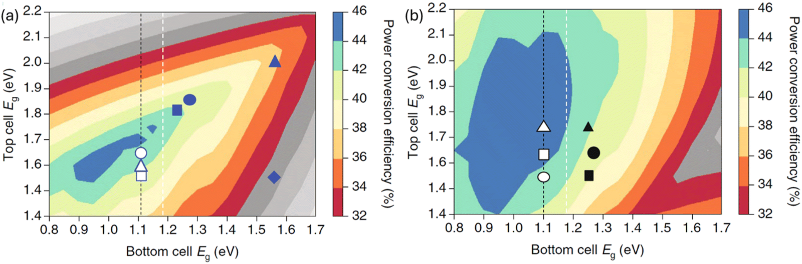 | ||
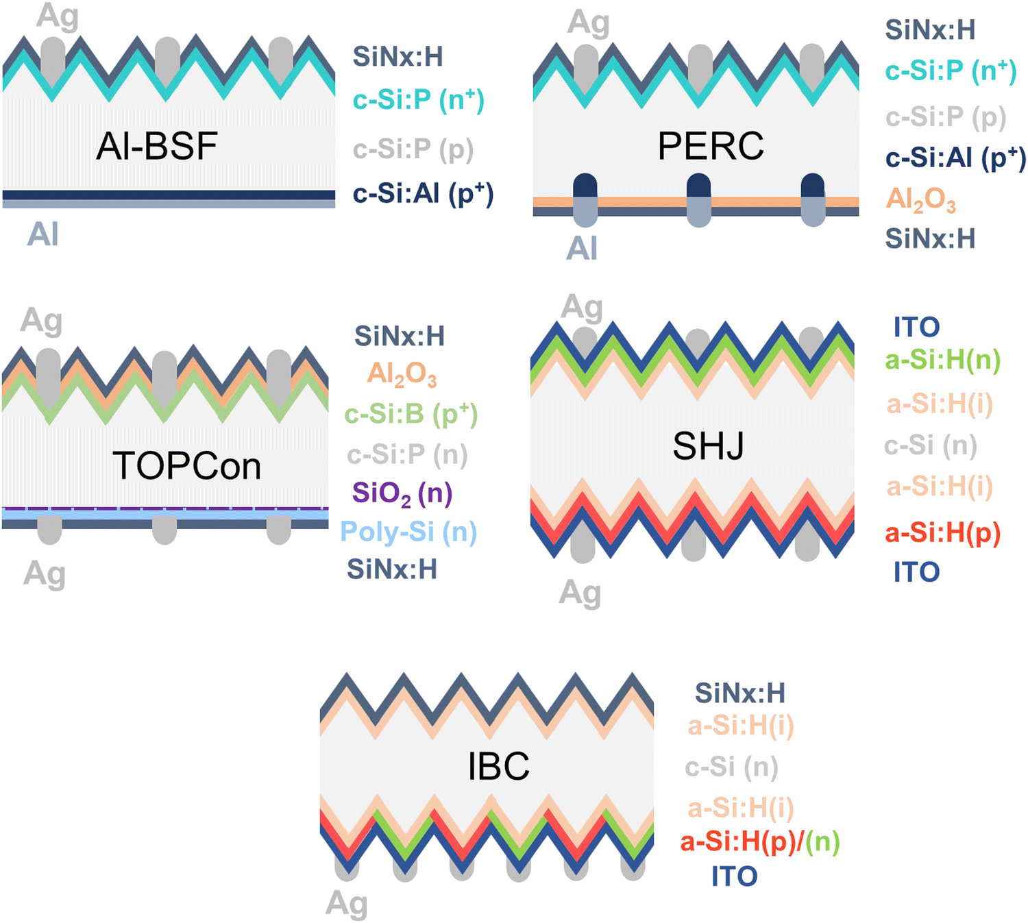
| Fig. 7 Theoretical performance for (a) 2T and (b) 4T TSCs, calculated with different Eg for top and bottom cells. Grey shading regions show lower device performance of TSCs than that of Shockly–Queisser limit of 32% for single junction with Eg of 1.1 eV. The open symbols represent the Eg combination for the best performance of 2T and 4T PSK-Si TSCs.13 Reproduced with permission, Copyright 2018, Nature Publishing Group. | ||
In the case of the chalcogenide absorber family due to their narrow Eg of Se-based compounds such as CISe, CIGSe, AIGSe, and Cu(In,Al)Se2, with Eg < 1.2 eV, are not well suited as top cells even if they have high PCE. However, pure ‘S’ based absorber layers such as CIS, CIGS, and CGS can be used as top cells. CIS (Eg = 1.5 eV) and CIGS (Eg = 1.57 eV) have a compatible Eg but still can achieve the PCE ∼30% for 2T devices. In contrast, CGS has a wide Eg of 2.5 eV, suitable for use as a top cell in triple junction TSCs. The ‘Se’ based chalcopyrite CGSe has the most favorable Eg and can be tuned with a Ga/Se ratio from 1.65 to 1.85![[thin space (1/6-em)]](https://www.rsc.org/images/entities/char_2009.gif) eV, making it a promising top cell for Si TSCs.229 In the case of the kesterite family, Eg values for Cu2MgSnS4, Cu2FeSnS4, Cu2CoSnS4, CBTS, and Cu2SrSnS4 are estimated to be approximately 1.6, 1.2, 1.11, 2.11, and 1.8 eV, respectively. Zn-substituted CXTS-inspired absorbers, such as those substituted by Mn, Mg, Fe, Ba, and Sr, appear promising as top cells with Eg close to 1.6 eV. The highest PCE pure ‘S’ based CZTS absorber has Eg around 1.55 eV, while the most efficient CZTSSe absorber with >15% PCE exhibits Eg around 1.1 eV.57 Thus, pure S-based CXTS absorbers with tunable Egvia partial or complete cation substitution in CXTS have a strong potential to make in Si-based TSCs with predicted PCE ∼35%. Followingly, in binary chalcogenides, such as GeS, Sb2S3 has an experimentally reported Eg ranging from 1.6–1.9 eV. GeSe, Sb2Se3, and SnS have an Eg of 1.1–1.3 eV, eliminating them from top cell competition. The experimentally reported values for SnS lie between 1.1–1.7 eV, possibly due to the co-existence of a secondary phase like SnS2, which has an Eg of 2.2–2.4 eV. Thus, for binary chalcogenides, like GeS and Sb2S3 with an Eg of around 1.7–1.8 eV, perfectly withstanding the ideal tandem top cell, though for high PCE Si-based TSCs, their Eg can be tuned with Se to match well with 1.65 eV required for bottom cell. They can also potentially deliver theoretically predicted PCE over 35–40% with a well-developed single-junction SCs device fabrication strategy.
eV, making it a promising top cell for Si TSCs.229 In the case of the kesterite family, Eg values for Cu2MgSnS4, Cu2FeSnS4, Cu2CoSnS4, CBTS, and Cu2SrSnS4 are estimated to be approximately 1.6, 1.2, 1.11, 2.11, and 1.8 eV, respectively. Zn-substituted CXTS-inspired absorbers, such as those substituted by Mn, Mg, Fe, Ba, and Sr, appear promising as top cells with Eg close to 1.6 eV. The highest PCE pure ‘S’ based CZTS absorber has Eg around 1.55 eV, while the most efficient CZTSSe absorber with >15% PCE exhibits Eg around 1.1 eV.57 Thus, pure S-based CXTS absorbers with tunable Egvia partial or complete cation substitution in CXTS have a strong potential to make in Si-based TSCs with predicted PCE ∼35%. Followingly, in binary chalcogenides, such as GeS, Sb2S3 has an experimentally reported Eg ranging from 1.6–1.9 eV. GeSe, Sb2Se3, and SnS have an Eg of 1.1–1.3 eV, eliminating them from top cell competition. The experimentally reported values for SnS lie between 1.1–1.7 eV, possibly due to the co-existence of a secondary phase like SnS2, which has an Eg of 2.2–2.4 eV. Thus, for binary chalcogenides, like GeS and Sb2S3 with an Eg of around 1.7–1.8 eV, perfectly withstanding the ideal tandem top cell, though for high PCE Si-based TSCs, their Eg can be tuned with Se to match well with 1.65 eV required for bottom cell. They can also potentially deliver theoretically predicted PCE over 35–40% with a well-developed single-junction SCs device fabrication strategy.
Over the years perovskite-based absorbers in Si tandem technology present ease of fining tuning of Eg with the help of halide ions to achieve current matching in 2T TSCs.230,231 Matter of fact in the chalcogenide community a well-established fine Eg tuning strategy is strongly needed to achieve the desired Eg. Different Eg grading strategies such as V-shape grading, grading in space charge region (front interface), or at the rear interface are reported to maximize PCE.232 In the case of CIGS and CIGSe TFSCs different Eg grading strategies during absorber growth have shown some success with modification in In, Ga, and S ratios. But the elements such as S and Se which dominantly affect the band position and modify the Eg properties, haven’t been proposed. Thus, GeS, Sb2S3, CXTS, and CGSe are the most promising absorber materials and are in line to be part of Si tandem technology with their Eg values. And it would be interesting to see their progress in single junction alongside Si-based TSCs technology.
We now consider the emerging chalcogenide single junction SCs and their theoretically achievable Jsc(S–Q) that can fulfill the current matching criteria. Interestingly, most chalcogenide-based absorbers have already achieved more than 75% of their Jsc(S–Q), however, it is inferior to those of high-performance absorbers such as c-Si, PSK, GaAs, CIGS, and CdTe, which are well above 90%. Emerging absorber materials such as GeS, SnS, AgBiS2, CGSe, and Sb2(S,Se)3 with relatively wider Eg (>1.5 eV) have their Jsc(S–Q) nearly 70–80% range and still need further improvement. Nonetheless, the most efficient chalcogenide-based TFSCs generate enough Jsc that can be considered as the top cell for 2T and 4T Si-based TSCs. Materials with wider Eg like GeS, CGSe, or Sb2S3 currently have relatively lower Jsc than the 2T current matching criteria shown in Fig. 8(a), Table 3, and Table S3 in ESI,† but it can be tweaked further with fine Eg and thickness tuning and absorber properties improvement.
 | ||
| Fig. 8 Reported champion cell parameters compared to the detailed-balance limit of single-junction SCs as a function of Eg (a) Short-circuit current (Jsc), (b) open-circuit voltage (Voc), (c) required top cell efficiency in Si-based TSCs to achieve 25, 27.5, and 30% efficiencies, respectively.21 The filled symbol shows the previous chalcogenide PCE and the hollow symbol shows the recent PCE. Reproduced with permission, Copyright 2014, IEEE, (d) transmittances of top cell vs. the device performance of 4T Si-based TSCs under different efficiencies of top cell.233 Reproduced with permission, Copyright 2019, Royal Society of Chemistry. Detailed-balance limit of single-junction SCs as a function of band gap for (e) PCE and (f) j vs. v × f. | ||
| Top cell material (example) | Top cell Eg (eV) | V oc (V) | J sc (mA cm−2) | Predicted tandem PCE |
|---|---|---|---|---|
| CGSe, BaZrS3, | 1.6–1.8 eV | 1.1–1.3 V | 15–20 mA cm−2 | 30–33% |
| Sb2S3 | 1.7–1.8 eV | 1.3–1.6 V | 15–18 mA cm−2 | 35–40% |
| CdTe, CZTS | 1.5 eV | ∼1.0 V | ∼18–20 mA cm−2 | ∼30% |
V oc: 2T and 4T TSCs require all sub-cells to achieve their best Voc to maximize tandem PCE. Some chalcogenides have outstanding optoelectronic properties for the required top-cell absorber materials; however, their current PCEs lag the value needed for the top cell of efficient 2T TSCs (see Fig. 8(b)). The main reason for this inferior PCE is the high Voc-deficit (defined as Eg/q-Voc) characteristics.27Fig. 8(b) shows the Voc of different chalcogenide TFSCs placed at a theoretically achievable Voc(S–Q) for their corresponding Eg. The overall scenario shows that only GaAs and PSK with recent PCE development have achieved more than 94% of their Voc(S–Q), while c-Si has achieved about 88% of its Voc(S–Q). A recent development from ‘EMPA’ and the ‘First Solar’ pushed the CIGSe and CdTe to Voc(S–Q) >75%, while the rest of the chalcogenide, except CIGSe lies in the 50–75% limit. The chalcogenides with narrow Eg show lower Voc loss, while wide Eg suffers higher Voc loss. Among the emerging chalcogenide absorber layers like Sb2(S,Se)3, AgBiS2, and CZTS remains near 50%, which needs concentrated development in the absorber layer to boost the Voc and PCE.
PCE: The high PEC of the top cell is another critical factor because the top cell can provide a large fraction (∼2/3) of the energy of the total tandem system.234Fig. 8(c) shows the required efficiency of the top cell in 2T Si-based TSCs to yield 25, 27.5, and 30% PCE, respectively, based on top cell parameters like Eg, diffusion length, absorption coefficient, and FF.21 Studies indicate that the top cell with a wide Eg only absorbs a small fraction of the incident photons, maximizing the PCE of the Si bottom cell. As a result, a top cell having Eg in the range of 1.5–1.7 eV must exhibit more than 15% to achieve 25% Si-based TSCs PCE. While reaching beyond 27.5 and 30% tandem efficiency, 17.5 and 20% top cell PCE are required in a similar Eg range. The gray shaded area shows that the current PCE of some chalcogenide TFSCs was reviewed by White et al.21 has been upgraded further and is approaching the theoretical value required beyond 25% PCE of single junction Si SCs. Another factor to consider for TSC design is light management for the sub-cells. The bottom cell in the TSCs only receives the illumination transmitted through the top cell. A chalcogenide-based absorber layer typically has absorption coefficients above its Eg on the order of 104 to 105 cm−1,235,236 and has discernible parasitic absorption below Eg due to defects and impurity phases. Consequently, the trade-off between sufficient absorption of high-energy photons and transmission of low-energy photons in the top cell needs to be tailored. Fig. 8(d) shows the transmittance of the top cell vs. the device PCEs of 4T Si-based TSCs under various top cell PCEs. Over 80% transmittances are required for the top cell with an Eg of 1.5 eV having PCE of 8%, to achieve a higher PCE in TSCs than in single-junction Si SCs. Ultimately, relaxed transmittance in the top cell achieves over 25% PCE in tandem configurations if the top cell exceeds 22% PCE.
The above situation gives an idea about the required top cell PCE while controlling transmittance. However, the current situation of single junction emerging chalcogenide-based SCs is well below the criteria. We have plotted the device parameters of some of the champion emerging chalcogenide-based SCs and well-established PV systems with respect to S–Q limit and categorized them into the different PV technologies, which are (i) high-performance ηS–Q >75%, (ii) moderate performance ηS–Q 75–50% and (iii) low-performance ηS–Q <50%. Fig. 8(e) shows that only PSK, c-Si, and GaAs have achieved more than ηS–Q >75%. On the other hand, the rest of the chalcogenide community struggles with PCE and resides below 50% of ηS–Q, except CIGSe, and CdTe. As explained earlier, the PCE of the emerging chalcogenide-based absorber layer must be improved to withstand competition in Si-based TSCs technology for top cell competition. We have calculated the S–Q limit for the corresponding device for each device parameter based on their reported Eg value (see Table S3). The lower PCE compared with the S–Q limit can be clearly identified as a large Voc loss. To further identify key issues in the poor performance reason and give ideas about further improvement, we plotted the j(Jsc/J(S–Q)) versus v × f (Voc × FF/Voc(S–Q) × FF(S–Q)) for all the reported champion emerging absorber materials along with ultra-high PCE PV materials (Fig. 8(f)). It provides insight into whether the PCE is limited by light management or charge carrier management. The ratio j(Jsc/J(S–Q)) reveals the Jsc losses coming from the light coupling, absorption, and trapping in the active layers from the top cell, followed by its carrier collection efficiency. The voltage ratio v = Voc/VS–Q shows the dominance of the carrier's recombination losses from the bulk, surfaces, and interfaces. Altogether (v × f), the voltage ratio and fill factor ratio f = FF/FFS–Q indicate the total electrical limitations of a cell. As expected, the j and v × f ratio approach unity for c-Si, GaAs, and PSK PVs and have good light and carrier management. In contrast, some chalcopyrites like CIGSe and CdTe are in moderate regions (0.5–0.75) situated in the upper regime, indicating these absorber materials have well-light management but need focused research on carrier management. This can be achieved through improved interface passivation, enhanced carrier extraction, and effective bulk defect suppression strategies to further boost Voc and reach the theoretical maximum PCE limited by non-radiative losses. Interestingly, the rest of the chalcogenide absorber materials exhibit j well beyond 0.7, ranging from 0.7–0.9, but scattered across the v × f far below 0.6, indicating the poor PCE is mainly limited by the bulk and interfaces as shown in Fig. 8(f). In other words, the high concentration of intrinsic defects, related defect clusters, band tailing (especially kesterite-based compounds), inherent deep-level defects, and high interface-assisted recombination rates (i.e., lattice mismatch, contamination of impurities, and dangling bonds at the interface) are believed to be the main causes of Voc loss and poor absorber quality for chalcogenide-based top cells.65,237,238 In particular, the abundant intrinsic defects and defect clusters can cause a significant downward shift of CB edge and non-radiative recombination, resulting in a large Voc loss.27,237 Moving forward, the typical minority carrier lifetime reported for high PCE devices remains in the range of 1–10 μs to 100–200 ns, while those for emerging chalcogenide absorber materials come several orders lower ∼1–10 ns or less due to dominant defect assisted non-radiative carrier recombination. The high carrier density, resulting from a large concentration of shallow acceptor-like defects, along with low hole mobility, limits efficient charge transport in the absorber layer. This leads to increased non-radiative recombination, reducing carrier lifetime and extraction. In addition, the low hole mobility also lowers the carrier collection probability, which is very high in the emerging absorber layer. These factors show that better carrier management is needed for emerging chalcogenide absorber materials compared to light management.
5. Strategies to improve the PCE of emerging chalcogenide–Si TSCs
5.1. Low-temperature fabrication techniques to produce high-quality top cell
To produce high-quality 2T TSCs with high PCE, a key requirement is to produce a well-crystallized chalcogenide absorber layer with pure phase and low defect density. Despite the challenges in fabrication shown in Fig. 9, recent advancements in low-temperature processing of chalcogenide absorbers make it possible to develop efficient devices. These materials can be fabricated using both physical and chemical deposition methods, besides hybrid methods combining both techniques for optimized results, as explained below. | ||
| Fig. 9 Different challenges associated with emerging chalcogenide absorber top cell and Si bottom cell during TSC fabrication. | ||
Overall, physical deposition methods are essential for the precise and controlled fabrication of high-quality chalcogenide absorber layers. The vapor-phase growth of chalcogenide-based absorbers involves crucial stages like sublimation, decomposition, evaporation, and nucleation growth.264 During each of these steps, thermal energy is used to suppress energy barriers, and various techniques can modify these critical stages to optimize film quality. The melting temperature and vapor pressure of precursor materials significantly influence the deposition process. Materials like Sb2X3 and some chalcogenide PSK have lower melting points and higher vapor pressures compared to other absorbers like CIGS, CdTe, and Si. It makes them suitable for deposit via physical deposition techniques. Along with physical techniques, chemical methods can play a significant role in the fabrication of chalcogenide absorber layers. Solution-based approaches such as hydrothermal, spray pyrolysis, spin coating, and CBD have been shown to produce phase-pure, less-defective absorber films with promising PCEs (e.g., Sb2X3, and Cu-based chalcogenide).256,265 Hybrid approaches, where molecular inks are spin-coated followed by post-sulfurization, have also been demonstrated to yield high-quality absorber layers. These methods can further reduce the defect density, improve grain growth, and enhance the overall PCE of the device. Techniques such as spin coating and hydrothermal are suitable for lab-scale production and demonstration of 2T TSC, while other physical techniques like TE, ALD, CVD, and VTD are scalable industrial processes.266
5.2. Passivation of interface defects
There are several critical factors for determining PCE in SCs. One effective strategy for improving Voc-deficit characteristics in top cells is surface defect passivation. Passivation layers with favorable lattice constants and dielectric properties can significantly suppress non-radiative recombination at the heterojunction interface, thereby reducing Voc-deficit characteristics.267–269 Several materials, such as Al2O3, HfO2, TiO2, Al(OH)3, SnO2, (Zn,Sn)O, (Cd,Zn)S, CdO, Sb2O3, Sb2Cl3, (Zn,Ti)O2, and Zn(O,S) have been investigated as passivation layers at the heterojunction.270–272 Some dielectric passivation layers provide both chemical as well as field effect passivation. Normally, the high densities of dangling bonds from the surface of chalcogenide-based thin films and lattice mismatch easily form defects. These defects mainly deteriorate the photogenerated charge transport characteristics and result in high carrier recombination near the interface between chalcogenides/buffer and chalcogenide/transparent conductive electrode (TCEs) layers. These high interface defects assisted carrier recombination significantly affect the overall PEC of chalcogenide-based SCs. It can be investigated through transient absorption, photoluminescence (PL), Raman, admittance, and deep-level transient spectroscopy techniques.261,265,272–276 Several research articles have emphasized different interface defect passivation strategies and their mechanisms for chalcogenide-based SCs. Strategies such as the application of a dielectric passivation layer via ALD, solution sulfurization, heterojunction heat treatment, re-crystallization, and others, have been reported.277–280 The previous reports suggest defects such as (i) CIGS; Cu-, Ga-vacancies and related defect clusters (ii) CZTSSe; Cu-vacancy, CuZn and ZnSn anti-sites and related defect clusters, and (iii) Sb2(S,Se)3; Sb-, S- or Se- vacancies and SbS anti-sites are detrimental defects.272,275,276,281,282Upon applying a passivation layer or treatment, it interacts differently or follows distinct mechanisms. For example, ALD-deposited dielectric passivation layers provide both chemical and field-effect passivation. During the process, the oppositely charged species from ALD precursor cycles (half ALD cycles) may absorb onto the chalcogenide absorber surface, passivating dangling bonds. The fixed negative charge neutralizes positively charged defects, while positive precursor ions counteract negatively charged defects at the interface. Additionally, the fixed negative charge repels electrons from the interface, suppressing recombination near positively charged defects. This dual effect enhances both chemical and field-effect passivation.279,280,283–285 For example, applying an Al2O3 layer using the ALD process provides chemical passivation through the ‘H’ generated during the ALD cycles. Additionally, excess ‘O’ during the initial growth of non-stoichiometric Al2O3 creates a negative charge, contributing to field-effect passivation. In kesterite, ‘Al’ precursor half cycles with trimethylaluminum facilitate the formation of a Cu-depleted nanolayer with a high density of ‘O’ and ‘Na’ accumulation at the surface (Fig. 10(a)). Similarly, ALD passivation combined with the air annealing process showed passivation of interface defects and pinholes in the absorber layer, reducing interface defect-assisted recombination, as verified by enhanced PL (Fig. 10(b)). Processes like heterojunction heat treatment demonstrate elemental interdiffusion mechanisms near the junction region, where the atoms from the buffer get diffused in the absorber layer passivating the defects. The well-known example of CdS/CZTS heat treatment shows ‘Cd’ occupies the ‘Zn’ site and passivates Zn-related anti-site defects (Fig. 10(c)).81 The solution-based treatment involves the spin coating of a passivation solution (cation or anion dissolved in aqueous or organic solvent) over the absorber layer followed by post-annealing steps. In Sb2S3, the coating of the SbCl3 layer on the Sb2S3 absorber layer showed the accumulation of ‘Sb’ and ‘Cl’ ions near the (130) Sb2S3 plane and defects. It modifies the work function and VBM of the absorber layer favoring efficient carrier transport near the Sb2S3/HTL interface (Fig. 10(d)). Whereas thioacetamide (TA) treatment drove the ‘S’ ions from the TA solution to occupy the chalcogenide absorber passivating ‘S’ vacancy or ‘O’ site (Fig. 10(e)).278 These strategies suppress the surface recombination velocity and improve the Voc and FF values in the device.286–292
 | ||
| Fig. 10 Various interface passivation strategies in chalcogenide absorber layers: (a) ALD-grown Al2O3 passivation on the CZTS absorber layer,286 Reproduced with permission, Copyright 2019, Royal Society of Chemistry, (b) photoluminescence spectra of ALD-passivated CZTS absorber layers with varying thicknesses and combinations with air annealing,293 Reproduced with permission, Copyright 2016, Wiley-VCH, (c) atomic-scale TEM image of the CdS/CZTS interface after heterojunction heat treatment,81 Reproduced with permission, Copyright 2018, Springer nature, (d) Sb and Cl iso-surface charge distribution around the (130) surface of Sb2S3 along with UPS spectra after Sb2Cl3 treatment,294 Reproduced with permission, Copyright 2020, American Chemical Society, and (e) schematic of solution sulfurization treatment with thioacetamide on Sb2S3 absorber layer, with corresponding XPS spectra before and after treatment.295 Reproduced with permission, Copyright 2019, Wiley-VCH. | ||
Fig. 11 shows Voc improvements for proven and emerging chalcogenide top cells by introducing various passivation layers. Notably, the combination of a sputtered Cd(O,S) passivation layer with a CBTS absorber resulted in a Voc improvement of over 40%.296 In the case of the Sb2S3-based top cells, Voc improvements ranging from 9.3 to 24% were achieved by introducing Sb2O3,297 (Zn,Ti)O2(ZTO),298,299 or Sb2Cl3300 as passivation layers. Additionally, the combinations of (i) Zn(O,S) with Cu(In,Ga)S2 and (ii) ZTO with CGSe demonstrated Voc improvements of 5.6 and 21.7%, respectively.76,301 However, the Voc-deficit values are still too large to achieve PCE over 16%. Previous reports suggest that complex deep-level defects in chalcogenides are the main reason for the Voc-deficit.268,296,302 Therefore, substantial efforts are needed to minimize defect-assisted recombination losses by developing and introducing novel and suitable passivation materials on chalcogenides.
 | ||
| Fig. 11 V oc improvements observed in proven and emerging material-based SCs with various passivation layers. Hollow symbols represent Voc without passivation layers, while filled symbols indicate Voc with passivation layers. Colors denote different passivation types: Red for oxide-based, Blue for sulfur-based, Pink for chlorine-based, and Gray for oxy-sulfide-based layers. | ||
5.3. Application of novel and excellent TCEs
TCEs are crucial components of TSCs. High optical transmittance (>90% in the visible wavelength) and low sheet resistance (10–25 Ω sq−1) are essential factors, always presenting a trade-off. Excellent electrical properties usually come with increased light absorption, leading to lower light transmission.296 In terms of device structure, the optoelectronic properties of top TCEs have a decisive influence on the PCE in 2T TSCs as both cells are electrically and mechanically connected.65 Experimentally, parasitic absorption loss from TCEs contributed to a photocurrent density loss of ∼1 mA cm−2 in 2T297 and 4–5 mA cm−2 in 4T203 TSCs. The parasitic absorption losses at the front TCE in 2T TSCs occur below 550 nm, while in 4T TSCs, they mainly occur in the near-infrared region (>800 nm) due to free carrier intra-band absorption.299 ZnO-based compounds such as i-ZnO/Al-doped ZnO (AZO) bi-layered TCEs, are typically used as top TCEs in chalcogenide single-junction SCs due to their low cost, excellent optoelectronic properties, and superior chemical and thermal stability. However, the preparation methods for ZnO-based top TCEs usually involve vacuum-based techniques (particularly the sputtering method), which can easily damage the thin buffer layer (typically less than 50–60 nm) during the deposition process.300 Locally formed damages for CBD-CdS were observed after the sputtering process, which is shown in Fig. 12(a–d). This indicates that the sputtering-induced damage to the CBD-CdS buffer is unavoidable and can be critical, particularly for thin layers. Therefore, less or no damage preparation techniques, such as vacuum- and solution-based approaches, have been widely established.301–304 These techniques should be deposited at low temperatures below 100 °C to avoid damaging the underlying layer. Another promising approach for minimizing damage during the preparation process involves two steps: (i) solution-based seed layer growth followed by (ii) vapor-based vacuum deposition growth.11 These approaches minimize unfavorable defects at interfaces in 2T TSCs. Unfortunately, the widely used AZO has limitations, such as a relatively narrow Eg (3.3 eV) and poor electrical resistivity (∼10−3 Ωcm), which restrict further improvements in PCE for chalcogenide-based single-junction SCs.300,305 To address these drawbacks, several high-performance TECs have been developed, including conductive polymers (i.e., PEDOT:PSS),306–308 metal (wire or mesh),309–311 metal oxides (ZnO, TiO2, or SnOxetc.),302,312 carbon-based materials (carbon nanotube (CNT)) and graphene),313,314 and dielectric/metal/dielectric structured materials.305,315–317 Excellent reviews covering the fundamentals, benefits, challenges, and their applications of each material have been reported.302,303,318–324Fig. 12(e) shows the optical transmittance vs. sheet resistance of previously reported and representative TCE materials. Despite the development of TCEs with excellent optoelectronic properties, several challenges remain to be addressed for their use in TSCs: | ||
| Fig. 12 Surface FE-SEM images of the CBD-CdS on a glass substrate after sputtering times of (a) 0, (b) 15, (c) 20, and (d) 30 min, respectively.300 Reproduced with permission, Copyright 2023, Wiley-VCH, (e) Optical transmittance vs. sheet resistance of reported TCEs such as ITO, metal oxide, metal wire or mesh, dielectric/metal/dielectric, CNT, graphene, PEDOT:PSS. | ||
One promising approach to overcome these drawbacks is combining the outstanding conductivity of metallic nanostructures with conducting polymers or carbon-based materials to create hybrid TCEs. This combination can lead to improved electronic properties as well as mechanical stability.
5.4. Application of suitable RL
In 2T-TSCs, the RL acts as the interconnection between the top and bottom cells, it plays a crucial role in achieving high PCEs.160 As both sub-cells are connected in series through their respective charge-collecting layers, efficient charge recombination is required for optimal performance. However, this 2T TSC configuration often leads to significant electrical losses due to interfacial resistance, which can reduce photocurrent collection and the Voc of the device. To mitigate such losses, designing suitable RLs with excellent optoelectronic properties is essential. One can consider the following factors to design a suitable RL (intermediate) in highly efficient TSCs.Fig. 13(a) shows the scheme, band alignment, and band position for CGSe-Si TSCs with a TCE interlayer as an RL (Intermediate). It shows a TCE interlayer with high conductivity that connects the top and bottom cells electrically, providing a high recombination site for charge carriers extracted from both cells. The introduction of reflective back contacts helps mitigate losses caused by differences in refractive index among the materials.13 Bush et al.11 successfully reported an extra Jsc of ∼1.5 mA cm−2 by introducing Si nanoparticles between a-Si and Ag reflector layers. In terms of band structure, photogenerated charge carriers move across each cell and then recombine at the TCE interlayer. The significant work function difference between the emitter material of the bottom Si cell and the TCE can create a high Schottky barrier, hindering electron flow from the emitter to the TCE and leading to poor device PCE. Minimizing the Schottky barrier by reducing the work function gap between the emitter in Si bottom cells and the TCE interlayer is essential. Unfortunately, the detailed studies on the band structure and alignments between recently developed TCEs as RL (intermediate) and emerging chalcogenide or buffer materials have not yet been sufficiently investigated. The excellent approaches for interconnecting layers as a recombination junction in all PSK and PSK-Si TSCs have been reported.13,177,326–328 Practically, oxide-based TCEs (ITO-, ZnO-based compounds, TiO2, and SnO2), metallic arrays (meshes, nanowire, and ultrathin layer), conductive composite (metal-coated polymethyl methacrylate (PMMA) and oxide-metal-oxide/organic-metal–organic frameworks), and conducting polymers (poly-3-hexylthiophene, polythermide, PEDOT:PSS, phenyl-C61-butyric acid methyl ester, Spiro-OMeTAD, carbon nanotubes, and graphene) have been utilized as RLs. Adaptable strategies for the intermediate layer as a recombination junction in chalcogenide–Si TSCs are as follows.
 | ||
| Fig. 13 Schemes, band alignments, and band positions for CGS-Si TSCs; (a) TEC and (b) tunnel junction as recombination junctions, respectively.227 Reproduced with permission, Copyright 2021, Wiley-VCH. | ||
The oxide-based TCEs with reduced reflection loss on the bottom Si should be developed. Typically, oxide-based TCEs have <10% reflections, resulting in a Jsc loss of approximately ∼2.2 mA cm−2.326,329 In this regard, hydrogen-doped ITO with reduced reflectance has been developed and applied to PSK-Si TSC by Knipp and co-workers.330 The authors also supported the optical simulation process to determine a realistic description of TSCs and achieved a high Jsc of over 20 mA cm−2. Normally, the preparation process of RLs includes vacuum-based techniques and they can mainly damage the Si bottom cells during the deposition process, resulting in poor performance in TSCs. Thus, promising strategies are introduced through low energy-based deposition processes such as solution-based approaches, ALD, soft sputtering, and CVD. The related research on outstanding performance has been investigated in TSCs.331–335 Secondly, metal-based alloys can be considered as RL's materials to realize the 2T TSCs owing to their excellent conductivity. Metal-based RL has been introduced mainly in III–V-Si TSC.160,336–338 Hidenori and co-workers reported the first meaningful demonstration by introducing Pd nanoparticles (less than 50 nm) between III–V and Si cells.339 Similarly, other metal nanoparticles have been employed in between III–V and Si cells as RLs, and it suppressed the reflectance loss and exhibited low transmittance loss (∼2%).340,341 However, the light loss from contact shading is still challenging. Conductive polymers, which include either long conjugated polymer chains or large macromolecules with many conjugated carbon rings, have been studied at all PSK and PSK-Si TSCs. They can easily form mechanical bonding between top and bottom cells, provide efficient transmission of sub-Eg photons, and good carrier collection and conduction. Brabec and co-worker introduced PEDOT:PSS layer as RL between PSK and Si cells and they achieved an excellent FF value of over 80%, PCE of 21.0% as well as negligible Voc loss compared to that of SC.342 Similarly, conductive composites (i.e., normally a combination of polymers and metal alloys) can also be considered as promising RL materials owing to their strong bonding ability and excellent conductivity in TSCs, and they have good mechanical strength, easy processing, and a minimal requirement on the bonding surface. For example, Tamboli and co-workers introduced an Ag-PMMA conductive composite as RL between GaInP and Si cells and they achieved a PCE of 26.4%.343 Here, Ag-PMMA conductive composite supported excellent carrier transport to each cell, high optical transmission, and good mechanical bonding. However, precise optical and electrical property controls are essential to optimize the PCE of TSCs.
The tunnel junction approach is well developed and provides an alternative to the recombination junction, effectively suppressing the optoelectronic loss originating from the TCE interlayer in Si-based TSCs.46,344 The low lateral conductivity of tunnel junction materials can effectively reduce the shunt path in TSC, which is a critical factor for the upscaling process. The high doping concentration in the P+–Si layer as a tunnel junction, as shown in Fig. 13(b), creates a relatively narrow depletion region, effectively promoting charge carriers to tunnel through the junction to recombine. Furthermore, the work function of tunnel junction materials should be investigated to ensure effective ohmic contact, which suggests the formation of adjacent n-type and p-type layers simultaneously in the TSCs.345 However, the recombination current density originating from the tunnel junction layer significantly suppresses the overall photocurrent density of tandems, which is a thorny challenge for improving PCE.
5.5. Maximizing light capture in TSCs
Light management, including reducing parasitic absorption losses and optimizing light incidence, is critical for further improving the overall PCE of TSCs. Firstly, parasitic absorption losses occur due to thick absorber layers and the absorbing characteristics of contact or interfacial layers and TCEs with high charge carrier absorption in near-infrared radiation.346 The design involving optical modeling can minimize the reflection peaks, allowing infrared radiation and visible light to be effectively absorbed by the bottom and top cells, respectively.347,348 However, challenges remain in the optical modeling, simulation, and practical experimental studies on suitable interfacial materials with various refractive indices to further improve PCE performance in emerging inorganic chalcogenide–Si TSCs.Secondly, improving light incidence can be achieved by introducing wide Eg interfacial materials (i.e., buffer, hole transfer layers, and TCEs), increasing the transmittance of top cells, and surface texture in bottom Si cells. Commonly, CBD-CdS has been widely used as a buffer layer due to its suitable Eg (∼2.4 eV) and favorable band alignment with a conduction band offset (CBO) value of +0.1–0.3 eV.49,233,300,305 However, the high absorption coefficient of CdS buffer results in a Jsc loss of about 1–2 mA cm−2.233 Simulations for kesterite-Si TSCs suggest a 4–14% relative reduction in the theoretical Jsc value. To improve light incidence in TSCs, extensive research and development of buffer materials with lower absorption coefficients, and wider and adjustable Eg are highly desirable. Wider Eg buffer materials show higher transmittance in the 350–500 nm wavelength range, leading to higher EQE (Fig. 14(a)), enhanced Voc value, and improved PCE performance. Although several investigations into wider Eg buffer materials have been conducted for emerging inorganic chalcogenide single-junction SCs, their PCE performance has not yet matched that of CdS buffer due to improper band alignments (i.e., large CBO value).
 | ||
| Fig. 14 (a) EQE spectra of kesterite-based single-junction SCs with different buffer layers.233 Reproduced with permission, Copyright 2019, Royal Society of Chemistry, (b) device performances of TSCs as a function of Eg and transmittance of top cells.349 Reproduced with permission, Copyright 2021, Elsevier. | ||
The incidence of light on the bottom Si cell is primarily limited by the Eg of the top cell, as only photons with energy greater than Eg can reach the bottom cell. The PCE of TSCs is determined by adjusting the Eg, CBO, and transmittance in the top cell, as shown in Fig. 14(b). The PCE for TSCs decreases with increasing Eg in the top cell. Top cells with PCE ranging from 13 to 15%, Eg from 1.55 to 1.7 eV, and high transmittance over 85% have already been achieved, increasing the PCE of TSCs from 0.4 to 1.5% compared to the bottom Si cell alone.233 However, a wider Eg and over 80% of transmittance in the top cell are still insufficient to achieve PCE performance for TSCs over 26%.
5.6. Long-terms stability, large-scale production, and outdoor test
The PCE degradation of TSCs is a critical factor in producing low-cost electricity.350,351 It is essential to have a deep understanding and insight into degradation mechanisms to achieve long-term stability. For Si-based single-junction SCs, degradation mechanisms have been extensively investigated, with the main causes being mechanical stress, cracked cells, snail trails, hot spots, and high voltage damage (Fig. 15(a–c)), potential induced degradation, light-induced degradation, and light and elevated temperature induced degradation.352–356 | ||
| Fig. 15 (a) Photograph of snail trails,357 Reproduced with permission, Copyright 2021, Elsevier. (b) Thermal infrared photograph on Si module.352 Reproduced with permission, Copyright 2022, Willey-VCH (c) Photograph of CdTe module after voltage stress of −1000 V during 1043 h under damp heat test conditions, reproduced with permission, copyright 2021, SPIE.358 (d) Damp heat test results for CIGS SCs without and with encapsulation and passivation of Al2O3.359 Reproduced with permission, Copyright 2018, Elsevier, (e) Long-term device performance of Si SCs under indoor and outdoor conditions.360 Reproduced with permission, Copyright 2021, Elsevier. | ||
Most of these degradation issues have been resolved, and commercialized Si-based single-junction SCs can secure a PCE of over 80% with a warranted lifetime of over 25 years.350 However, emerging inorganic chalcogenide-based single-junction SCs remain less extensively studied and have not achieved long-term stability like Si SCs. The stability failure summary of chalcogenide absorbers, including CIGS, CZTSSe, and Sb2(S,Se)3, is shown in Table S4 and Note 2, ESI.† For kesterite and Sb2(S,Se)3 the instability of the charge transport layer (HTL/ETL) or the degradation of the TCO layer is reported as the main cause of stability failure. Among inorganic chalcogenides, the CIGSe-based single-junction SCs have been relatively well investigated.352,359 Their common failure mode includes alkali elements migration and buffer, and TCO layer degradation. One promising approach for improving long-term stability involves introducing H2O-resistant inorganic thin layers (i.e., Al2O3, TiO2, and SnO2) between polymeric front and back sheets as encapsulation materials (Fig. 15(d)).361,362 The CIGS-based module without encapsulation shows a considerable loss in FF during the first 100 h of damp heat testing, primarily due to shunt paths from the degradation of AZO. In contrast, the ALD-Al2O3 encapsulated CIGSe-based module showed better long-term stability over 2000 h of damp heat testing due to reduced humidity penetration.
All PV devices are installed outdoors, making long-term stability investigations crucial for achieving cost-effective electricity. Carigiet et al.363 reported an interesting review of long-term stability for Si-based modules under indoor and outdoor conditions. The annual degradation rate was estimated to be 0.29 ± 0.06% for a string in indoor conditions, while that of outdoor conditions (0.18 ± 0.06%) was lower, as shown in Fig. 15(e). However, the difference between indoor and outdoor conditions is negligible and represents only one site result. Therefore, more comparative research is needed to analyze various conditions comprehensively. Unfortunately, higher annual PCE degradation rates per year for single-junction SCs (i.e., HIT cells) have been reported, highlighting the need for in-depth investigation and insight into long-term stability for emerging inorganic chalcogenides.
6. Summary and perspective
This review discusses emerging inorganic chalcogenide-based Si TSCs as a promising solution to the PCE and long-term stability limitations faced by single-junction SCs. We began by outlining the current status and issues with single-junction SCs and existing TSC technologies needed for the development of emerging inorganic chalcogenide–Si TSCs. Subsequently, we briefly summarized the principles of TSCs (i.e., maximum light utilization of light, suitable interconnecting layers, optical design, Eg, and stacking orders) and current challenges for previously reported III–V-Si and PSK-Si TSCs. In Section 3, we focused on the optoelectronic properties (Table 1) and current PCE status (Fig. 2) of proven chalcogenides (i.e., chalcopyrite, kesterite, and Sb2S3), emerging chalcogenides (i.e., group IV metal binary and I–V–VI2 ternary compounds), and chalcogenide PSKs. The different optoelectronic properties and single-junction SCs PCE progress give brief ideas and research directions for chalcogenide-based absorber materials suitable for TSCs. We then explored the opportunities for Si as a suitable bottom cell and potential top candidates in emerging chalcogenide–Si TSC. In addition to highlighting some promising progress in CZTS-Si, CGSe-Si, and Sb2S3-Si tandems, the Eg-based evaluation of different chalcogenide absorbers showed absorbers such as CGSe and Sb2S3 can be promising materials with close match Eg values of 1.65–1.75 eV. Finally, following the recent progress, we discussed the key challenges and potential solutions for emerging inorganic chalcogenide–Si TSCs including fabrication complexity, achieving well-matched Eg in each cell, improving top cell efficiency, reducing recombination losses, maximizing light capture, ensuring long-term stability, and the need for outdoor performance testing. This review not only provides new insights into promising inorganic material systems as top cells in the Si-based TSCs but also outlines further research direction for early-stage development and commercialization of these promising emerging inorganic chalcogenide–Si TSCs.Data availability
No primary research results, software or code have been included, and no new data were generated or analyzed as part of this review.Conflicts of interest
There are no conflicts to declare.Acknowledgements
This work was primarily supported by the Australian Research Council through the Discovery Early Career Researcher Award (DECRA) (DE210101565) and the Discovery Project (DP230101676). Additional support was provided in part by the National Research Foundation of Korea (NRF) (grant no. 2023R1A2C2003612) and the National R&D programs through the Korea Institute of Energy Research (KIER) (grant no. C5-2414) and partly supported by Korea Institute of Energy Technology Evaluation and Planning (KETEP) grant funded by the Korea government (No. 20213030010340). This material is also based on work supported by the U.S. Air Force Research Laboratory under agreement number FA9453–19-C-1002. The views expressed herein are those of the authors and do not necessarily reflect those of the Australian Research Council. The U.S. Government is authorized to reproduce and distribute reprints for governmental purposes notwithstanding any copyright notation thereon. The views and conclusions contained herein are those of the authors and should not be interpreted as necessarily representing official policies or endorsements of the U.S. Air Force Research Laboratory or the U.S. Government.References
- M. A. Green, Nat. Energy, 2016, 1, 1–4 Search PubMed.
- S. Sivaraj, R. Rathanasamy, G. V. Kaliyannan, H. Panchal, A. Jawad Alrubaie, M. Musa Jaber, Z. Said and S. Memon, Energies, 2022, 15, 8688 CrossRef CAS.
- W. Shockley and H. J. Queisser, J. Appl. Phys., 1961, 32, 510 CrossRef CAS.
- A. W. Y. Ho-Baillie, J. Zheng, M. A. Mahmud, F.-J. Ma, D. R. McKenzie and M. A. Green, Appl. Phys. Rev., 2021, 8, 041307 CAS.
- P. Kumar, S. Thokala, S. P. Singh and R. Singh, Nano Energy, 2024, 121, 109175 CrossRef CAS.
- K. Alberi, J. J. Berry, J. J. Cordell, D. J. Friedman, J. F. Geisz, A. R. Kirmani, B. W. Larson, W. E. Mcmahon, L. M. Mansfield, P. F. Ndione, M. Owen-Bellini, A. F. Palmstrom, M. O. Reese, S. B. Reese, M. A. Steiner, A. C. Tamboli, S. Theingi and E. L. Warren, Joule, 2024, 8, 658–692 CrossRef.
- H. Li and W. Zhang, Chem. Rev., 2020, 120, 9835–9950 CrossRef CAS PubMed.
- J. F. Geisz, R. M. France, K. L. Schulte, M. A. Steiner, A. G. Norman, H. L. Guthrey, M. R. Young, T. Song and T. Moriarty, Nat. Energy, 2020, 5, 326–335 CrossRef CAS.
- M. N. Sharif, J. Yang, X. Zhang, Y. Tang and K. F. Wang, Solar RRL, 2023, 7, 2300156 CrossRef CAS.
- X. Liu, J. Zhang, L. Tang, J. Gong, W. Li, Z. Ma, Z. Tu, Y. Li, R. Li, X. Hu, C. Shen, H. Wang, Z. Wang, Q. Lin, G. Fang, S. Wang, C. Liu, Z. Zhang, J. Li and X. Xiao, Energy Environ. Sci., 2023, 16, 5029–5042 RSC.
- K. A. Bush, A. F. Palmstrom, Z. J. Yu, M. Boccard, R. Cheacharoen, J. P. Mailoa, D. P. McMeekin, R. L. Z. Hoye, C. D. Bailie, T. Leijtens, I. M. Peters, M. C. Minichetti, N. Rolston, R. Prasanna, S. Sofia, D. Harwood, W. Ma, F. Moghadam, H. J. Snaith, T. Buonassisi, Z. C. Holman, S. F. Bent and M. D. McGehee, Nat. Energy, 2017, 2, 1–7 Search PubMed.
- C. U. Kim, E. D. Jung, Y. W. Noh, S. K. Seo, Y. Choi, H. Park, M. H. Song and K. J. Choi, EcoMat, 2021, 3, e12084 CrossRef CAS.
- T. Leijtens, K. A. Bush, R. Prasanna and M. D. McGehee, Nat. Energy, 2018, 3, 828–838 CrossRef CAS.
- K. Dolia, S. Neupane, S. Fu, Y. Yin, A. Abudulimu, A. Rahimi, M. Hattarki, B. Dokken, T. Zhu, A. Adhikari, M. K. Jamarkattel, R. E. Irving, A. B. Phillips, M. J. Heben, R. J. Ellingson, Y. Yan and Z. Song, Solar RRL, 2024, 2400148 CrossRef CAS.
- E.-B. Kim, M. S. Akhtar, C. Liu, Y. Wang and S. Ameen, J. Mater. Chem. A, 2024, 12, 12262–12273 RSC.
- HZB Sets New World Record for CIGS Perovskite Tandem Solar Cells – Helmholtz-Zentrum Berlin (HZB), https://www.helmholtz-berlin.de/pubbin/news_seite?nid=28846&sprache=en&seitenid=1, (accessed 15 March 2025).
- H. Liang, J. Feng, C. D. Rodríguez-Gallegos, M. Krause, X. Wang, E. Alvianto, R. Guo, H. Liu, R. K. Kothandaraman, R. Carron, A. N. Tiwari, I. M. Peters, F. Fu and Y. Hou, Joule, 2023, 7, 2859–2872 CrossRef CAS.
- Interactive Best Research-Cell Efficiency Chart|Photovoltaic Research|NREL, https://www.nrel.gov/pv/interactive-cell-efficiency.html, (accessed 25 May 2024).
- M. A. Green, E. D. Dunlop, M. Yoshita, N. Kopidakis, K. Bothe, G. Siefer and X. Hao, Prog. Photovoltaics Res. Appl., 2024, 32, 3–13 CrossRef.
- Longi claims 34.6% efficiency for perovskite-silicon tandem solar cell – pv magazine International, https://www.pv-magazine.com/2024/06/14/longi-claims-34-6-efficiency-for-perovskite-silicon-tandem-solar-cell/, (accessed 17 June 2024).
- T. White, N. Lal and K. Catchpole, IEEE J. Photovoltaics, 2014, 4, 208–214 Search PubMed.
- M. A. Fazal and S. Rubaiee, Sol. Energy, 2023, 258, 203–219 CrossRef.
- L. Duan, D. Walter, N. Chang, J. Bullock, D. Kang, S. P. Phang, K. Weber, T. White, D. Macdonald, K. Catchpole and H. Shen, Nat. Rev. Mater., 2023, 8, 261–281 CrossRef CAS.
- C. Messmer, B. S. Goraya, S. Nold, P. S. C. Schulze, V. Sittinger, J. Schön, J. C. Goldschmidt, M. Bivour, S. W. Glunz and M. Hermle, Prog. Photovoltaics Res. Appl., 2021, 29, 744–759 CrossRef CAS.
- H. Zhang, X. Fu, Y. Tang, H. Wang, C. Zhang, W. W. Yu, X. Wang, Y. Zhang and M. Xiao, Nat. Commun., 2019, 10, 1088 CrossRef CAS PubMed.
- W. Mao, C. R. Hall, S. Bernardi, Y. B. Cheng, A. Widmer-Cooper, T. A. Smith and U. Bach, Nat. Mater., 2020, 20, 55–61 CrossRef PubMed.
- S. Hadke, M. Huang, C. Chen, Y. F. Tay, S. Chen, J. Tang and L. Wong, Chem. Rev., 2022, 122, 10170–10265 CrossRef CAS PubMed.
- F. Liu, Q. Zeng, J. Li, X. Hao, A. Ho-Baillie, J. Tang and M. A. Green, Mater. Today, 2020, 41, 120–142 CrossRef CAS.
- B. Saparov, Chem. Rev., 2022, 122, 10575–10577 CrossRef CAS PubMed.
- J. W. Turnley and R. Agrawal, Chem. Commun., 2024, 60, 5245–5269 RSC.
- M. A. Green, E. D. Dunlop, M. Yoshita, N. Kopidakis, K. Bothe, G. Siefer, X. Hao and J. Y. Jiang, Prog. Photovoltaics Res. Appl., 2025, 33, 3–15 CrossRef.
- V. Karade, A. Lokhande, P. Babar, M. G. Gang, M. Suryawanshi, P. Patil and J. H. Kim, Sol. Energy Mater. Sol. Cells, 2019, 200, 109911 CrossRef CAS.
- E. Raza and Z. Ahmad, Energy Rep., 2022, 8, 5820–5851 CrossRef.
- F. Larsson, N. S. Nilsson, J. Keller, C. Frisk, V. Kosyak, M. Edoff and T. Törndahl, Prog. Photovoltaics Res. Appl., 2017, 25, 755–763 CrossRef CAS.
- G. Regmi, A. Ashok, P. Chawla, P. Semalti, S. Velumani, S. N. Sharma and H. Castaneda, J. Mater. Sci.: Mater. Electron., 2020, 31, 7286–7314 CrossRef CAS.
- M. Hermle, F. Feldmann, M. Bivour, J. C. Goldschmidt and S. W. Glunz, Appl. Phys. Rev., 2020, 7, 021305 CAS.
- Z. Zhang, Z. Li, L. Meng, S. Y. Lien and P. Gao, Adv. Funct. Mater., 2020, 30, 2001904 CrossRef CAS.
- Z. Wang, Z. Song, Y. Yan, S. (Frank) Liu and D. Yang, Adv. Sci., 2019, 6, 1801704 CrossRef PubMed.
- S. Resalati, T. Okoroafor, A. Maalouf, E. Saucedo and M. Placidi, Appl. Energy, 2022, 313, 118888 CrossRef CAS.
- M. F. Mohamad Noh, N. A. Arzaee, C. C. Fat, T. Sieh Kiong, M. A. Mat Teridi and A. W. Mahmood Zuhdi, Mater. Today Energy, 2024, 39, 101473 CrossRef CAS.
- S. Akhil, S. Akash, A. Pasha, B. Kulkarni, M. Jalalah, M. Alsaiari, F. A. Harraz and R. G. Balakrishna, Mater. Des., 2021, 211, 110138 CrossRef CAS.
- Y. Ko, H. Park, C. Lee, Y. Kang, Y. Jun, Y. Ko, C. Lee, Y. Kang, Y. Jun and H. Park, Adv. Mater., 2020, 32, 2002196 CrossRef CAS PubMed.
- J. H. Park, S. K. Hwang, S. G. Ji and J. Y. Kim, Exploration, 2023, 3, 20220029 CrossRef PubMed.
- H. Li and W. Zhang, Chem. Rev., 2020, 120, 9835–9950 CrossRef CAS PubMed.
- O. Ramírez, E. M. Lanzoni, R. G. Poeira, T. P. Weiss, R. Leturcq, A. Redinger and S. Siebentritt, APL Mater., 2022, 10, 61108 CrossRef.
- M. Nakamura, K. Yamaguchi, Y. Kimoto, Y. Yasaki, T. Kato and H. Sugimoto, IEEE J. Photovoltaics, 2019, 9, 1863–1867 Search PubMed.
- K. S. Gour, V. Karade, P. Babar, J. Park, D. M. Lee, V. N. Singh and J. H. Kim, Solar RRL, 2021, 5, 2000815 CrossRef CAS.
- E. M. Mkawi, Results Phys., 2020, 19, 103603 CrossRef.
- G. U. Kamble, S. W. Shin, S. W. Park, M. A. Gaikwad, V. C. Karade, J. S. Jang, Y. Park, U. V. Ghorpade, M. P. Suryawanshi and J. H. Kim, Solar RRL, 2023, 7, 2300502 CrossRef CAS.
- L. A. Burton, D. Colombara, R. D. Abellon, F. C. Grozema, L. M. Peter, T. J. Savenije, G. Dennler and A. Walsh, Chem. Mater., 2013, 25, 4908–4916 CrossRef CAS.
- E. Barrios Salgado, D. Eréndira Lara Llanderal, M. T. S. Nair, W. Zhang, Y. Cheng, J. Zhao, Y. Gupta, P. Arun, I. Suzuki, S. Kawanishi, T. Omata and H. Yanagi, J. Phys.: Energy, 2022, 4, 042002 Search PubMed.
- L. Mehdaoui, R. Miloua, M. Khadraoui, M. O. Bensaid, D. Abdelkader, F. Chiker and A. Bouzidi, Phys. B, 2019, 564, 114–124 CrossRef CAS.
- M. Choi, S. Kim, M. Lee, J. S. Yun, V. C. Karade, J. Lim, J. Y. Yang and J. Park, J. Mater. Chem. A, 2024, 12, 16831–16838 RSC.
- A. M. Medina-Gonzalez, B. A. Rosales, U. H. Hamdeh, M. G. Panthani and J. Vela, Chem. Mater., 2020, 32, 6085–6096 CrossRef CAS.
- M. Kumar, A. Singh, D. Gill and S. Bhattacharya, J. Phys. Chem. Lett., 2021, 12, 5301–5307 CrossRef CAS PubMed.
- K. V. Sopiha, C. Comparotto, J. A. Márquez and J. J. S. Scragg, Adv. Opt. Mater., 2022, 10, 2101704 CrossRef CAS.
- O. Almora, G. C. Bazan, C. I. Cabrera, L. A. Castriotta, S. Erten-Ela, K. Forberich, K. Fukuda, F. Guo, J. Hauch, A. W. Y. Ho-Baillie, T. J. Jacobsson, R. A. J. Janssen, T. Kirchartz, R. R. Lunt, X. Mathew, D. B. Mitzi, M. K. Nazeeruddin, J. Nelson, A. F. Nogueira, U. W. Paetzold, B. P. Rand, U. Rau, T. Someya, C. Sprau, L. Vaillant-Roca, C. J. Brabec, O. Almora, C. J. Brabec, G. C. Bazan and L. A. Castriotta, Adv. Energy Mater., 2024, 2404386 Search PubMed.
- O. Almora, D. Baran, G. C. Bazan, C. I. Cabrera, S. Erten-Ela, K. Forberich, F. Guo, J. Hauch, A. W. Y. Ho-Baillie, T. J. Jacobsson, R. A. J. Janssen, T. Kirchartz, N. Kopidakis, M. A. Loi, R. R. Lunt, X. Mathew, M. D. McGehee, J. Min, D. B. Mitzi, M. K. Nazeeruddin, J. Nelson, A. F. Nogueira, U. W. Paetzold, B. P. Rand, U. Rau, H. J. Snaith, E. Unger, L. Vaillant-Roca, C. Yang, H. L. Yip and C. J. Brabec, Adv. Energy Mater., 2022, 13, 2203313 CrossRef.
- O. Almora, C. I. Cabrera, S. Erten-Ela, K. Forberich, K. Fukuda, F. Guo, J. Hauch, A. W. Y. Ho-Baillie, T. J. Jacobsson, R. A. J. Janssen, T. Kirchartz, M. A. Loi, X. Mathew, D. B. Mitzi, M. K. Nazeeruddin, U. W. Paetzold, B. P. Rand, U. Rau, T. Someya, E. Unger, L. Vaillant-Roca and C. J. Brabec, Adv. Energy Mater., 2024, 14, 2303173 CrossRef CAS.
- R. K. Yadav, P. S. Pawar, Y. T. Kim, I. Sharma and J. Heo, J. Mater. Chem. A, 2024, 12, 3265–3275 RSC.
- S. Barthwal, R. Kumar and S. Pathak, ACS Appl. Energy Mater., 2022, 5, 6545–6585 CrossRef CAS.
- Y. Zhou, L. Wang, S. Chen, S. Qin, X. Liu, J. Chen, D. J. Xue, M. Luo, Y. Cao, Y. Cheng, E. H. Sargent and J. Tang, Nat. Photonics, 2015, 9, 409–415 CrossRef CAS.
- R. Kondrotas, C. Chen and J. Tang, Joule, 2018, 2, 857–878 CrossRef CAS.
- X. Liu, Z. Cai, L. Wan, P. Xiao, B. Che, J. Yang, H. Niu, H. Wang, J. Zhu, Y. T. Huang, H. Zhu, S. J. Zelewski, T. Chen, R. L. Z. Hoye and R. Zhou, Adv. Mater., 2024, 36, 2305841 CrossRef CAS PubMed.
- U. Ali Shah, S. Chen, G. Mohamed Gomaa Khalaf, Z. Jin, H. Song, U. A. Shah, S. Chen, G. M. G. Khalaf, Z. Jin and H. Song, Adv. Funct. Mater., 2021, 31, 2100265 CrossRef.
- M. R. Filip, C. E. Patrick and F. Giustino, Phys. Rev. B: Condens. Matter Mater. Phys., 2013, 87, 205125 CrossRef.
- S. Wang, Y. Zhao, B. Che, C. Li, X. Chen, R. Tang, J. Gong, X. Wang, G. Chen, T. Chen, J. Li and X. Xiao, Adv. Mater., 2022, 34, 2206242 CrossRef CAS PubMed.
- R. Tang, X. Wang, C. Jiang, S. Li, G. Jiang, S. Yang, C. Zhu and T. Chen, J. Mater. Chem. A, 2018, 6, 16322–16327 RSC.
- Y. Huang, H. Gao, X. Peng, G. Wang, P. Xiao, B. Che, R. Tang, C. Zhu and T. Chen, Solar RRL, 2023, 7, 2201115 CrossRef CAS.
- L. Zhang, W. Lian, X. Zhao, Y. Yin, T. Chen and C. Zhu, ACS Appl. Energy Mater., 2020, 3, 12417–12422 CrossRef CAS.
- C. Jiang, R. Tang, X. Wang, H. Ju, G. Chen and T. Chen, Solar RRL, 2019, 3, 1800272 CrossRef.
- G. Shen, A. Ke, S. Chen, T. Ma, S. Ali, M. Li, H. Y. Hsu, C. Chen, P. Yang, H. Song and J. Tang, Adv. Energy Mater., 2025, 2406051 CrossRef.
- Y. Zhao, W. Xu, J. Wen, X. Wang, X. Chen, B. Che, H. Wang, J. Gong, T. Chen, X. Xiao, J. Li, Y. Zhao, X. Chen, J. Gong, X. Xiao, J. Li, W. Xu, J. Wen, X. Wang, B. Che, H. Wang and T. Chen, Adv. Mater., 2024, 36, 2410669 CrossRef CAS PubMed.
- S. Suresh and A. R. Uhl, Adv. Energy Mater., 2021, 11, 2003743 CrossRef CAS.
- B. J. Stanbery, Crit. Rev. Solid State Mater. Sci., 2002, 27, 73–117 CrossRef CAS.
- S. Shukla, M. Sood, D. Adeleye, S. Peedle, G. Kusch, D. Dahliah, M. Melchiorre, G. M. Rignanese, G. Hautier, R. Oliver and S. Siebentritt, Joule, 2021, 5, 1816–1831 CrossRef CAS.
- S. Ishizuka, A. Yamada, P. J. Fons, H. Shibata and S. Niki, Prog. Photovoltaics, 2014, 22, 821–829 CAS.
- A. Walsh, S. Chen, S. H. Wei and X. G. Gong, Adv. Energy Mater., 2012, 2, 400–409 CrossRef CAS.
- T. Gershon, K. Sardashti, O. Gunawan, R. Mankad, S. Singh, Y. Seog Lee, J. A. Ott, A. Kummel and R. Haight, Adv. Energy Mater., 2016, 6, 1601182 CrossRef.
- L. Weston and C. Stampfl, Phys. Rev. Mater., 2018, 2, 085407 CrossRef CAS.
- C. Yan, J. Huang, K. Sun, S. Johnston, Y. Zhang, H. Sun, A. Pu, M. He, F. Liu, K. Eder, L. Yang, J. M. Cairney, N. J. Ekins-Daukes, Z. Hameiri, J. A. Stride, S. Chen, M. A. Green and X. Hao, Nat. Energy, 2018, 3, 764–772 CrossRef CAS.
- S. Das and P. Mahanandia, Mater. Chem. Phys., 2022, 281, 125878 CrossRef CAS.
- P. Fan, J. Lin, J. Hu, Z. Yu, Y. Zhao, S. Chen, Z. Zheng, J. Luo, G. Liang, Z. Su, P. Fan, J. Lin, J. Hu, Z. Yu, Y. Zhao, S. Chen, Z. Zheng, J. Luo, G. Liang and Z. Su, Adv. Funct. Mater., 2022, 32, 2207470 CrossRef CAS.
- P. Sinsermsuksakul, L. Sun, S. Woon Lee, H. Hejin Park, S. Bok Kim, C. Yang, R. G. Gordon, P. Sinermsuksakul, S. B. Kim, R. G. Gordon, L. Sun, H. H. Park, C. Yang and S. S. W. Lee, Adv. Energy Mater., 2014, 4, 1400496 CrossRef.
- H. S. Yun, B. Wook Park, Y. C. Choi, J. Im, T. J. Shin and S. Il Seok, Adv. Energy Mater., 2019, 9, 1901343 CrossRef.
- D. Lim, H. Suh, M. Suryawanshi, G. Yeom Song, J. Yu Cho, J. Hyeok Kim, J. Hyuck Jang, C.-W. Jeon, A. Cho, S. Ahn, J. Heo, D. Lim, M. Suryawanshi, G. Y. Song, J. Y. Cho, J. H. Kim, J. Heo, H. Suh, J. H. Jang, C. Jeon, A. Cho and S. Ahn, Adv. Energy Mater., 2018, 8, 1702605 CrossRef.
- S. C. Liu, C. M. Dai, Y. Min, Y. Hou, A. H. Proppe, Y. Zhou, C. Chen, S. Chen, J. Tang, D. J. Xue, E. H. Sargent and J. S. Hu, Nat. Commun., 2021, 12, 1–7 CrossRef PubMed.
- K. Wang, H. Ni, W. Zhao, X. Wu, Y. Hu, G. Xiao and F. Jiang, Energy Environ. Sci., 2023, 16, 1155–1165 RSC.
- D. J. Xue, S. C. Liu, C. M. Dai, S. Chen, C. He, L. Zhao, J. S. Hu and L. J. Wan, J. Am. Chem. Soc., 2017, 139, 958–965 CrossRef CAS PubMed.
- P. Sinsermsuksakul, R. Chakraborty, S. B. Kim, S. M. Heald, T. Buonassisi and R. G. Gordon, Chem. Mater., 2012, 24, 4556–4562 CrossRef CAS.
- G. Radovsky, R. Popovitz-Biro, M. Staiger, K. Gartsman, C. Thomsen, T. Lorenz, G. Seifert, R. Tenne, M. Staiger, C. Thomsen, T. Lorenz and G. Seifert, Angew. Chem., 2011, 123, 12524–12528 CrossRef.
- A. Rabkin, S. Samuha, R. E. Abutbul, V. Ezersky, L. Meshi and Y. Golan, Nano Lett., 2015, 15, 2174–2179 CrossRef CAS PubMed.
- P. Sinsermsuksakul, J. Heo, W. Noh, A. S. Hock and R. G. Gordon, Adv. Energy Mater., 2011, 1, 1116–1125 CrossRef CAS.
- Z. Deng, D. Cao, J. He, S. Lin, S. M. Lindsay and Y. Liu, ACS Nano, 2012, 6, 6197–6207 CrossRef CAS PubMed.
- S. Sovizi, S. Angizi, S. A. Ahmad Alem, R. Goodarzi, M. R. R. Taji Boyuk, H. Ghanbari, R. Szoszkiewicz, A. Simchi and P. Kruse, Chem. Rev., 2023, 123, 13869–13951 CrossRef CAS PubMed.
- B. Mukherjee, E. S. Tok and C. H. Sow, J. Appl. Phys., 2013, 114, 134302 CrossRef.
- S. C. Liu, C. M. Dai, Y. Min, Y. Hou, A. H. Proppe, Y. Zhou, C. Chen, S. Chen, J. Tang, D. J. Xue, E. H. Sargent and J. S. Hu, Nat. Commun., 2021, 12, 1–7 CrossRef PubMed.
- Y. T. Huang, S. R. Kavanagh, M. Righetto, M. Rusu, I. Levine, T. Unold, S. J. Zelewski, A. J. Sneyd, K. Zhang, L. Dai, A. J. Britton, J. Ye, J. Julin, M. Napari, Z. Zhang, J. Xiao, M. Laitinen, L. Torrente-Murciano, S. D. Stranks, A. Rao, L. M. Herz, D. O. Scanlon, A. Walsh and R. L. Z. Hoye, Nat. Commun., 2022, 13, 1–13 Search PubMed.
- S. Akhil and R. G. Balakrishna, J. Mater. Chem. A, 2022, 10, 8615–8625 RSC.
- Y. Wang, S. R. Kavanagh, I. Burgués-Ceballos, A. Walsh, D. Scanlon and G. Konstantatos, Nat. Photonics, 2022, 16, 235–241 CrossRef CAS.
- M. Bernechea, N. C. Miller, G. Xercavins, D. So, A. Stavrinadis and G. Konstantatos, Nat. Photonics, 2016, 10, 521–525 CrossRef CAS.
- Y. Wang, L. Peng, Z. Wang and G. Konstantatos, Adv. Energy Mater., 2022, 12, 2200700 CrossRef CAS.
- S. L. Diedenhofen, M. Bernechea, K. M. Felter, F. C. Grozema and L. D. A. Siebbeles, Solar RRL, 2019, 3, 1900075 CrossRef.
- P. C. Huang, W. C. Yang and M. W. Lee, J. Phys. Chem. C, 2013, 117, 18308–18314 CrossRef CAS.
- S. N. Guin and K. Biswas, Chem. Mater., 2013, 25, 3225–3231 CrossRef CAS.
- L. Mehdaoui, R. Miloua, M. Khadraoui, M. O. Bensaid, D. Abdelkader, F. Chiker and A. Bouzidi, Phys. B, 2019, 564, 114–124 CrossRef CAS.
- F. Viñes, M. Bernechea, G. Konstantatos and F. Illas, Phys. Rev. B, 2016, 94, 235203 CrossRef.
- S. Geller and J. H. Wernick, Acta Crystallogr., 1959, 12, 46–54 CrossRef CAS.
- A. C. Glatz and A. Pinella, J. Mater. Sci., 1968, 3, 498–501 CrossRef CAS.
- F. Viñes, G. Konstantatos and F. Illas, Phys. Chem. Chem. Phys., 2017, 19, 27940–27944 RSC.
- A. Zanatta and I. Chambouleyron, Phys. Rev. B:Condens. Matter Mater. Phys., 1996, 53, 3833 CrossRef CAS PubMed.
- L. Mehdaoui, R. Miloua, M. Khadraoui, M. O. Bensaid, D. Abdelkader, F. Chiker and A. Bouzidi, Phys. B, 2019, 564, 114–124 CrossRef CAS.
- B. Pejova, I. Grozdanov, D. Nesheva and A. Petrova, Chem. Mater., 2008, 20, 2551–2565 CrossRef CAS.
- X. Li, H. Yu, X. Ma, Z. Liu, J. Huang, Y. Shen and M. Wang, Chem. Eng. J., 2024, 495, 153328 CrossRef CAS.
- R. Syam Kumar, A. Akande, F. El-Mellouhi, H. Park and S. Sanvito, Phys. Rev. Mater., 2020, 4, 075401 CrossRef.
- L. P. A. Maia, J. S. Souza, A. F. Lima and M. V. Lalic, Opt. Mater., 2024, 148, 114927 CrossRef CAS.
- B. A. Rosales, M. A. White and J. Vela, J. Am. Chem. Soc., 2018, 140, 3736–3742 CrossRef CAS PubMed.
- Y. T. Huang, M. Schleuning, H. Hempel, Y. Zhang, M. Rusu, T. Unold, A. Musiienko, O. Karalis, N. Jung, S. J. Zelewski, A. J. Britton, N. Ngoh, W. Song, L. C. Hirst, H. Sirringhaus, S. D. Stranks, A. Rao, I. Levine and R. L. Z. Hoye, Adv. Funct. Mater., 2024, 2310283 CrossRef CAS.
- B. V. Gabrel’yan, A. A. Lavrentiev, I. Y. Nikiforov and V. V. Sobolev, J. Struct. Chem., 2008, 49, 788–794 CrossRef.
- A. M. Medina-Gonzalez, P. Yox, Y. Chen, M. A. S. Adamson, B. A. Rosales, M. Svay, E. A. Smith, R. D. Schaller, K. Wu, A. J. Rossini, K. Kovnir and J. Vela, Chem. Mater., 2022, 34, 7357–7368 CrossRef CAS.
- A. D. Jodlowski, D. Rodríguez-Padrón, R. Luque, G. de Miguel, A. D. Jodlowski, G. De Miguel and D. Rodríguez, Adv. Energy Mater., 2018, 8, 1703120 CrossRef.
- D. Tiwari, O. S. Hutter and G. Longo, J. Phys.: Energy, 2021, 3, 034010 CAS.
- A. Swarnkar, W. J. Mir, R. Chakraborty, M. Jagadeeswararao, T. Sheikh and A. Nag, Chem. Mater., 2019, 31, 565–575 CrossRef CAS.
- Y. Nishigaki, T. Nagai, M. Nishiwaki, T. Aizawa, M. Kozawa, K. Hanzawa, Y. Kato, H. Sai, H. Hiramatsu, H. Hosono and H. Fujiwara, Solar RRL, 2020, 4, 1900555 CrossRef CAS.
- S. Niu, H. Huyan, Y. Liu, M. Yeung, K. Ye, L. Blankemeier, T. Orvis, D. Sarkar, D. J. Singh, R. Kapadia, J. Ravichandran, S. Niu, H. Huyan, Y. Liu, K. Ye, T. Orvis, J. Ravichandran, M. Yeung, L. Blankemeier, D. Sarkar, R. Kapadia, M. Hsieh and D. J. Singh, Adv. Mater., 2017, 29, 1604733 CrossRef PubMed.
- M. T. Hörantner and H. J. Snaith, Energy Environ. Sci., 2017, 10, 1983–1993 RSC.
- J. A. Brehm, J. W. Bennett, M. R. Schoenberg, I. Grinberg and A. M. Rappe, J. Chem. Phys., 2014, 140, 224703 CrossRef PubMed.
- K. C. Vincent, S. Agarwal, J. W. Turnley and R. Agrawal, Adv. Energy Sustainability Res., 2023, 4, 2300010 CrossRef CAS.
- T. Gupta, D. Ghoshal, A. Yoshimura, S. Basu, P. K. Chow, A. S. Lakhnot, J. Pandey, J. M. Warrender, H. Efstathiadis, A. Soni, E. Osei-Agyemang, G. Balasubramanian, S. Zhang, S. F. Shi, T. M. Lu, V. Meunier and N. Koratkar, Adv. Funct. Mater., 2020, 30, 2001387 CrossRef CAS.
- Y. Y. Sun, M. L. Agiorgousis, P. Zhang and S. Zhang, Nano Lett., 2015, 15, 581–585 CrossRef CAS PubMed.
- W. Meng, B. Saparov, F. Hong, J. Wang, D. B. Mitzi and Y. Yan, Chem. Mater., 2016, 28, 821–829 CrossRef CAS.
- J. A. Márquez, M. Rusu, H. Hempel, I. Y. Ahmet, M. Kölbach, I. Simsek, L. Choubrac, G. Gurieva, R. Gunder, S. Schorr and T. Unold, J. Phys. Chem. Lett., 2021, 12, 2148–2153 CrossRef PubMed.
- X. Wei, H. Hui, C. Zhao, C. Deng, M. Han, Z. Yu, A. Sheng, P. Roy, A. Chen, J. Lin, D. F. Watson, Y. Y. Sun, T. Thomay, S. Yang, Q. Jia, S. Zhang and H. Zeng, Nano Energy, 2020, 68, 104317 CrossRef CAS.
- Y. Han, J. Xu, Y. Liang, X. Chen, M. Jia, J. Zhang, L. Lian, Y. Liu, X. Li and Z. Shi, Chem. Eng. J., 2023, 473, 145351 CrossRef CAS.
- E. Osei-Agyemang, N. Koratkar and G. Balasubramanian, J. Mater. Chem. C, 2021, 9, 3892–3900 RSC.
- V. K. Ravi, S. H. Yu, P. K. Rajput, C. Nayak, D. Bhattacharyya, D. S. Chung and A. Nag, Nanoscale, 2021, 13, 1616–1623 RSC.
- U. V. Ghorpade, M. P. Suryawanshi, M. A. Green, T. Wu, X. Hao and K. M. Ryan, Chem. Rev., 2023, 123, 327–378 CrossRef CAS PubMed.
- F. Palazon, Solar RRL, 2022, 6, 2100829 CrossRef CAS.
- I. Caño, J. W. Turnley, P. Benítez, C. López-Álvarez, J. M. Asensi, D. Payno, J. Puigdollers, M. Placidi, C. Cazorla, R. Agrawal and E. Saucedo, J. Mater. Chem. C, 2024, 12, 3154–3163 RSC.
- J. He, X. Hu, Z. Liu, W. Chen and G. Longo, Adv. Funct. Mater., 2023, 33, 2306075 CrossRef CAS.
- Y. C. Choi and K. W. Jung, Nanomaterials, 2020, 10, 2284 CrossRef CAS PubMed.
- D. Savytskii, M. Sanders, R. Golovchak, B. Knorr, V. Dierolf and H. Jain, J. Am. Ceram. Soc., 2014, 97, 198–205 CrossRef CAS.
- Y. Wang, X. Dai, C. Dong, W. Guo, Z. Xu, Y. Chen, H. Xiang and R. Zhang, Adv. Mater., 2022, 34, 2106773 CrossRef CAS PubMed.
- K. T. Butler, S. McKechnie, P. Azarhoosh, M. Van Schilfgaarde, D. O. Scanlon and A. Walsh, Appl. Phys. Lett., 2016, 108, 112103 CrossRef.
- H. Akkus, A. M. Mamedov, A. Kazempour and H. Akbarzadeh, Cent. Eur. J. Phys., 2008, 6, 64–75 CAS.
- R. Nitsche and W. J. Merz, J. Phys. Chem. Solids, 1960, 13, 154–155 CrossRef CAS.
- Solar - IEA, https://www.iea.org/energy-system/renewables/solar-pv, (accessed 22 May 2024).
- B. V. Stefani, M. Kim, Y. Zhang, B. Hallam, M. A. Green, R. S. Bonilla, C. Fell, G. J. Wilson and M. Wright, Joule, 2023, 7, 2684–2699 CrossRef.
- H. Lin, M. Yang, X. Ru, G. Wang, S. Yin, F. Peng, C. Hong, M. Qu, J. Lu, L. Fang, C. Han, P. Procel, O. Isabella, P. Gao, Z. Li and X. Xu, Nat. Energy, 2023, 8, 789–799 CrossRef CAS.
- LONGi sets new world record with 27.30% for heterojunction back contact cells and renames next generation silicon tera wafer to TaiRay Wafer, https://www.longi.com/eu/news/2730-hbc-world-record/, (accessed 15 March 2025).
- G. M. Wilson, M. Al-Jassim, W. K. Metzger, S. W. Glunz, P. Verlinden, G. Xiong, L. M. Mansfield, B. J. Stanbery, K. Zhu, Y. Yan, J. J. Berry, A. J. Ptak, F. Dimroth, B. M. Kayes, A. C. Tamboli, R. Peibst, K. Catchpole, M. O. Reese, C. S. Klinga, P. Denholm, M. Morjaria, M. G. Deceglie, J. M. Freeman, M. A. Mikofski, D. C. Jordan, G. Tamizhmani and D. B. Sulas-Kern, J. Phys. D: Appl. Phys., 2020, 53, 493001 CrossRef CAS.
- P. G. V. Sampaio and M. O. A. González, Renewable Sustainable Energy Rev., 2017, 74, 590–601 CrossRef.
- J. Day, S. Senthilarasu and T. K. Mallick, Renew Energy, 2019, 132, 186–205 CrossRef.
- M. C. Raval, S. M. Reddy and A. Hegedus, Industrial Silicon Solar Cells, in Solar Cells, ed. H. S. Nalwa, IntechOpen, London, 2019, ch. 1.
- T. G. Allen, J. Bullock, X. Yang, A. Javey and S. De Wolf, Nat. Energy, 2019, 4, 914–928 CrossRef CAS.
- D. K. Ghosh, S. Bose, G. Das, S. Acharyya, A. Nandi, S. Mukhopadhyay and A. Sengupta, Surf. Interfaces, 2022, 30, 101917 CrossRef CAS.
- E. Aydin, T. G. Allen, M. De Bastiani, A. Razzaq, L. Xu, E. Ugur, J. Liu and S. De Wolf, Science, 1979, 2024(383), 1–13 Search PubMed.
- M. I. Elsmani, N. Fatima, M. P. A. Jallorina, S. Sepeai, M. S. Suait, N. A. Ludin, M. A. M. Teridi, K. Sopian and M. A. Ibrahim, Nanomaterials, 2021, 11, 3186 CrossRef CAS PubMed.
- M. Wright, B. Vicari Stefani, T. W. Jones, B. Hallam, A. Soeriyadi, L. Wang, P. Altermatt, H. J. Snaith, G. J. Wilson and R. S. Bonilla, Energy Environ. Sci., 2023, 16, 4164–4190 RSC.
- P. Zhang, C. Li, M. He, Z. Liu and X. Hao, Small Methods, 2024, 8, 2300432 CrossRef CAS PubMed.
- M. De Bastiani, A. S. Subbiah, E. Aydin, F. H. Isikgor, T. G. Allen and S. De Wolf, Mater. Horiz., 2020, 7, 2791–2809 RSC.
- S. De Wolf and M. Kondo, J. Appl. Phys., 2009, 105, 103707 CrossRef.
- J. H. Park, S. G. Ji, Y. S. Yoon, M. A. Park, S. H. Lee, K. H. Kim and J. Y. Kim, Adv. Mater. Technol., 2023, 8, 2201006 CrossRef CAS.
- F. Fu, J. Li, T. C. J. Yang, H. Liang, A. Faes, Q. Jeangros, C. Ballif and Y. Hou, Adv. Mater., 2022, 34, 2106540 CrossRef CAS PubMed.
- G. Nogay, F. Sahli, J. Werner, R. Monnard, M. Boccard, M. Despeisse, F. J. Haug, Q. Jeangros, A. Ingenito and C. Ballif, ACS Energy Lett., 2019, 4, 844–845 CrossRef CAS.
- S. Yu, M. Rabelo and J. Yi, Trans. Electr. Electron. Mater., 2022, 23, 327–336 CrossRef.
- Y. Du, B. Xu, G. Wang, Y. Miao, B. Li, Z. Kong, Y. Dong, W. Wang and H. H. Radamson, Nanomaterials, 2022, 12, 741 CrossRef CAS PubMed.
- Philipps: McEvoy's Handbook of Photovoltaics - Google Scholar, https://scholar.google.com/scholar_lookup?hl=en&publication_year=2018&pages=439-472&author=S.+P.+Philipps&author=F.+Dimroth&author=A.+W.+Bett&title=McEvoy%27s+Handbook+of+Photovoltaics, (accessed 25 May 2024).
- X. Li, Q. Xu, L. Yan, C. Ren, B. Shi, P. Wang, S. Mazumdar, G. Hou, Y. Zhao and X. Zhang, Nanophotonics, 2021, 10, 2001–2022 CrossRef CAS.
- M. Akiyama, Y. Kawarada and K. Kaminishi, J. Cryst. Growth, 1984, 68, 21–26 CrossRef CAS.
- K. Derendorf, S. Essig, E. Oliva, V. Klinger, T. Roesener, S. P. Philipps, J. Benick, M. Hermle, M. Schachtner, G. Siefer, W. Jäger and F. Dimroth, IEEE J. Photovoltaics, 2013, 3, 1423–1428 Search PubMed.
- R. Cariou, J. Benick and P. Beutel, IEEE J. Photovoltaics, 2017, 7, 367–373 Search PubMed.
- Y. Zeng, Z. Ding, Z. Liu, Q. Zhou, X. Liu, Z. Liu, S. M. Iftiquar, J. Jung and J. Yi, J. Phys. D: Appl. Phys., 2018, 51, 133002 CrossRef.
- S. Essig, C. Allebé, T. Remo, J. F. Geisz, M. A. Steiner, K. Horowitz, L. Barraud, J. S. Ward, M. Schnabel, A. Descoeudres, D. L. Young, M. Woodhouse, M. Despeisse, C. Ballif and A. Tamboli, Nat. Energy, 2017, 2, 1–9 Search PubMed.
- P. Schygulla, R. Müller, D. Lackner, O. Höhn, H. Hauser, B. Bläsi, F. Predan, J. Benick, M. Hermle, S. W. Glunz and F. Dimroth, Prog. Photovoltaics Res. Appl., 2022, 30, 869–879 CrossRef CAS.
- M. N. Sharif, J. Yang, X. Zhang, Y. Tang and K. F. Wang, Solar RRL, 2023, 7, 2300156 CrossRef CAS.
- C. Gao, D. Du, D. Ding, F. Qiao and W. Shen, J. Mater. Chem. A, 2022, 10, 10811–10828 RSC.
- IEC 61215-1:2016 | IEC Webstore | rural electrification, solar power, solar panel, photovoltaic, PV, smart city, LVDC, https://webstore.iec.ch/publication/24312, (accessed 25 May 2024).
- New method allows perovskite solar cells to meet IEC testing requirements, https://www.iec.ch/blog/new-method-allows-perovskite-solar-cells-meet-iec-testing-requirements, (accessed 25 May 2024).
- A. K. Jena, A. Kulkarni and T. Miyasaka, Chem. Rev., 2019, 119, 3036–3103 CrossRef CAS PubMed.
- R. Wang, T. Huang, J. Xue, J. Tong, K. Zhu and Y. Yang, Nat. Photonics, 2021, 15, 411–425 CrossRef CAS.
- J. Wei, Q. Wang, J. Huo, F. Gao, Z. Gan, Q. Zhao and H. Li, Adv. Energy Mater., 2021, 11, 2002326 CrossRef CAS.
- Z. Wang, Z. Zhang, L. Xie, S. Wang, C. Yang, C. Fang and F. Hao, Adv. Opt. Mater., 2022, 10, 2101822 CrossRef CAS.
- P. Roy, N. Kumar Sinha, S. Tiwari and A. Khare, Sol. Energy, 2020, 198, 665–688 CrossRef CAS.
- C. Ran, Y. Wang, W. Gao, Y. Xia, Y. Chen and W. Huang, Solar RRL, 2021, 5, 2100665 CrossRef CAS.
- M. Ren, X. Qian, Y. Chen, T. Wang and Y. Zhao, J. Hazard. Mater., 2022, 426, 127848 CrossRef CAS PubMed.
- J. Qian, Sustainable Energy Fuels, 2019, 3, 1439–1447 RSC.
- R. Witteck, J. F. Geisz, E. L. Warren and W. E. McMahon, Solar RRL, 2024, 8, 2300782 CrossRef CAS.
- G. Ji, M.-A. Park, H. Jang, J. Y. Kim, I. J. Park, J. H. Park, S. G. Ji and J. H. Jang, Joule, 2019, 3, 807–818 CrossRef.
- Y. Shi, J. J. Berry and F. Zhang, ACS Energy Lett., 2024, 9, 1305–1330 CrossRef CAS.
- M. Abbas, X. Xu, M. Rauf and A. K. K. Kyaw, Photonics, 2024, 11, 87 CrossRef CAS.
- P. Chen, Y. Bai and L. Wang, Small Struct., 2021, 2, 2000050 CrossRef CAS.
- S. Mahesh, J. M. Ball, R. D. J. Oliver, D. P. McMeekin, P. K. Nayak, M. B. Johnston and H. J. Snaith, Energy Environ. Sci., 2020, 13, 258–267 RSC.
- C. Zhang, Y. N. Lu, W. Q. Wu and L. Wang, Nano Energy, 2021, 81, 105634 CrossRef CAS.
- M. Jošt, E. Köhnen, A. B. Morales-Vilches, B. Lipovšek, K. Jäger, B. Macco, A. Al-Ashouri, J. Krč, L. Korte, B. Rech, R. Schlatmann, M. Topič, B. Stannowski and S. Albrecht, Energy Environ. Sci., 2018, 11, 3511–3523 RSC.
- M. De Bastiani, R. Jalmood, J. Liu, C. Ossig, A. Vlk, K. Vegso, M. Babics, F. H. Isikgor, A. S. Selvin, R. Azmi, E. Ugur, S. Banerjee, A. J. Mirabelli, E. Aydin, T. G. Allen, A. Ur Rehman, E. Van Kerschaver, P. Siffalovic, M. E. Stuckelberger, M. Ledinsky and S. De Wolf, Adv. Funct. Mater., 2023, 33, 2205557 CrossRef CAS.
- S. Lu, C. Chen and J. Tang, Front. Optoelectron., 2020, 13, 246–255 CrossRef PubMed.
- (PDF) Toward A 25%-efficient polycrystalline thin-film tandem solar cell: Practical issues, https://www.researchgate.net/publication/4078364_Toward_A_25-efficient_polycrystalline_thin-film_tandem_solar_cell_Practical_issues, (accessed 23 May 2024).
- A. R. Jeong, S. Bin Choi, W. M. Kim, J. K. Park, J. Choi, I. Kim and J. H. Jeong, Sci. Rep., 2017, 7, 1–10 CrossRef CAS PubMed.
- K. Kim, J. Gwak, S. K. Ahn, Y. J. Eo, J. H. Park, J. S. Cho, M. G. Kang, H. E. Song and J. H. Yun, Sol. Energy, 2017, 145, 52–58 CrossRef CAS.
- T. Hölscher, M. Placidi, I. Becerril-Romero, R. Fonoll-Rubio, V. Izquierdo-Roca, A. Thomere, E. Bailo, T. Schneider, H. Kempa, R. Scheer and A. Pérez-Rodríguez, Sol. Energy Mater. Sol. Cells, 2023, 251, 112169 CrossRef.
- Y. Li, C. Cui, H. Wei, Z. Shao, Z. Wu, S. Zhang, X. Wang, S. Pang and G. Cui, Adv. Mater., 2024, 2400138 CrossRef CAS PubMed.
- M. Valentini, C. Malerba, L. Serenelli, M. Izzi, E. Salza, M. Tucci and A. Mittiga, Sol. Energy, 2019, 190, 414–419 CrossRef CAS.
- F. Martinho, A. Hajijafarassar, S. Lopez-Marino, M. Espíndola-Rodríguez, S. Engberg, M. Gansukh, F. Stulen, S. Grini, S. Canulescu, E. Stamate, A. Crovetto, L. Vines, J. Schou and O. Hansen, ACS Appl. Energy Mater., 2020, 3, 4600–4609 CrossRef CAS.
- A. Hajijafarassar, F. Martinho, F. Stulen, S. Grini, S. López-Mariño, M. Espíndola-Rodríguez, M. Döbeli, S. Canulescu, E. Stamate, M. Gansukh, S. Engberg, A. Crovetto, L. Vines, J. Schou and O. Hansen, Sol. Energy Mater. Sol. Cells, 2020, 207, 110334 CrossRef CAS.
- E. R. Weber, Impurity Precipitation, Dissolution, Gettering and Passivation in PV Silicon: Final Technical Report, 30 January 1998–29 August 2001.
- M. Gansukh, A. Assar, F. Martinho, S. L. Mariño, M. Espíndola-Rodríguez, S. Engberg, E. Stamate, J. Schou, O. Hansen and S. Canulescu, Appl. Phys. A:Mater. Sci. Process., 2022, 128, 1–6 CrossRef.
- A. Assar, F. Martinho, J. Larsen, N. Saini, D. Shearer, M. V. Moro, F. Stulen, S. Grini, S. Engberg, E. Stamate, J. Schou, L. Vines, S. Canulescu, C. Platzer-Björkman and O. Hansen, ACS Appl. Mater. Interfaces, 2022, 14, 14342–14358 CrossRef CAS PubMed.
- C. Qian, K. Sun, J. Cong, H. Cai, J. Huang, C. Li, R. Cao, Z. Liu, M. Green, B. Hoex, T. Chen and X. Hao, Adv. Mater., 2023, 35, 2303936 CrossRef CAS PubMed.
- Z. Xia, J. Zhong, M. Leng, L. Hu, D. J. Xue, B. Yang, Y. Zhou, X. Liu, S. Qin, Y. B. Cheng and J. Tang, Chem. Mater., 2015, 27, 8048–8057 CrossRef CAS.
- C. Gao, M. Xu, B. K. Ng, L. Kang, L. Jiang, Y. Lai and F. Liu, Mater. Lett., 2017, 195, 186–189 CrossRef CAS.
- M. Okil, A. Shaker, I. S. Ahmed, T. M. Abdolkader and M. S. Salem, Sol. Energy Mater. Sol. Cells, 2023, 253, 112210 CrossRef CAS.
- F. Martinho, Energy Environ. Sci., 2021, 14, 3840–3871 RSC.
- L. P. Mwakyusa, X. Jin, E. Müller, R. Schneider, D. Gerthsen, M. Rinke, U. W. Paetzold, B. S. Richards and M. Hetterich, J. Appl. Phys., 2021, 129, 153104 CrossRef CAS.
- P. Punathil, E. Artegiani, S. Zanetti, L. Lozzi, V. Kumar and A. Romeo, Sol. Energy, 2022, 236, 599–607 CrossRef CAS.
- M. Kumar, A. Dubey, N. Adhikari, S. Venkatesan and Q. Qiao, Energy Environ. Sci., 2015, 8, 3134–3159 RSC.
- Q. Cao, O. Gunawan, M. Copel, K. B. Reuter, S. J. Chey, V. R. Deline and D. B. Mitzi, Adv. Energy Mater., 2011, 1, 845–853 CrossRef CAS.
- U. Chalapathi, B. Poornaprakash and S. H. Park, Superlattices Microstruct., 2020, 141, 106500 CrossRef CAS.
- D. Alagarasan, S. S. Hegde, S. Varadharajaperumal, K. D. Arun Kumar, R. Naik, S. P. Panjalingam, E. E. S. Massoud and R. Ganesan, J. Mater. Sci.: Mater. Electron., 2022, 33, 4794–4805 CrossRef CAS.
- M. D. K. Jones, J. A. Dawson, S. Campbell, V. Barrioz, L. D. Whalley and Y. Qu, Front. Chem., 2022, 10, 920676 CrossRef CAS PubMed.
- M. He, C. Yan, J. Li, M. P. Suryawanshi, J. Kim, M. A. Green and X. Hao, Adv. Sci., 2021, 8, 2004313 CrossRef CAS PubMed.
- S. Akhil and R. G. Balakrishna, J. Mater. Chem. A, 2022, 10, 8615–8625 RSC.
- A. J. Bett, K. M. Winkler, M. Bivour, L. Cojocaru, Ö. Kabakli, P. S. C. Schulze, G. Siefer, L. Tutsch, M. Hermle, S. W. Glunz and J. C. Goldschmidt, ACS Appl. Mater. Interfaces, 2019, 11, 45796–45804 CrossRef CAS PubMed.
- X. Zhang, D. Han, S. Chen, C. Duan and J. Chu, J. Energy Chem., 2018, 27, 1140–1150 CrossRef.
- D. Colombara, H. Elanzeery, N. Nicoara, D. Sharma, M. Claro, T. Schwarz, A. Koprek, M. H. Wolter, M. Melchiorre, M. Sood, N. Valle, O. Bondarchuk, F. Babbe, C. Spindler, O. Cojocaru-Miredin, D. Raabe, P. J. Dale, S. Sadewasser and S. Siebentritt, Nat. Commun., 2020, 11, 1–14 CrossRef PubMed.
- B. Shin, N. A. Bojarczuk and S. Guha, Appl. Phys. Lett., 2013, 102, 091907 CrossRef.
- S. Prathapani and Y. Zhan, Energy Technol., 2021, 9, 2100193 CrossRef CAS.
- S. P. Bremner, M. Y. Levy and C. B. Honsberg, Prog. Photovoltaics Res. Appl., 2008, 16, 225–233 CrossRef.
- B. Mahmoudi, F. Caddeo, T. Lindenberg, T. Schneider, T. Hölscher, R. Scheer and A. W. Maijenburg, Electrochim. Acta, 2021, 367, 137183 CrossRef CAS.
- M. H. Miah, M. U. Khandaker, M. B. Rahman, M. Nur-E-Alam and M. A. Islam, RSC Adv., 2024, 14, 15876–15906 RSC.
- S. Tao, I. Schmidt, G. Brocks, J. Jiang, I. Tranca, K. Meerholz and S. Olthof, Nat. Commun., 2019, 10, 1–10 CrossRef CAS PubMed.
- I. Sharma, P. S. Pawar, R. Kumar Yadav, R. Nandi and J. Heo, Sol. Energy, 2022, 246, 152–180 CrossRef CAS.
- B. Vermang, G. Brammertz, M. Meuris, T. Schnabel, E. Ahlswede, L. Choubrac, S. Harel, C. Cardinaud, L. Arzel, N. Barreau, J. Van Deelen, P. J. Bolt, P. Bras, Y. Ren, E. Jaremalm, S. Khelifi, S. Yang, J. Lauwaert, M. Batuk, J. Hadermann, X. Kozina, E. Handick, C. Hartmann, D. Gerlach, A. Matsuda, S. Ueda, T. Chikyow, R. Félix, Y. Zhang, R. G. Wilks and M. Bär, Sustainable Energy Fuels, 2019, 3, 2246–2259 RSC.
- M. B. Salim, R. Nekovei and R. Jeyakumar, Sol. Energy, 2020, 198, 160–166 CrossRef.
- D. B. Mitzi and Y. Kim, Faraday Discuss., 2022, 239, 9–37 RSC.
- F. Werlinger, C. Segura, J. Martínez, I. Osorio-Roman, D. Jara, S. J. Yoon and A. F. Gualdrón-Reyes, Energies, 2023, 16, 5868 CrossRef CAS.
- D. Shin, B. Saparov and D. B. Mitzi, Adv. Energy Mater., 2017, 7, 1602366 CrossRef.
- A. Crovetto, S. Kim, M. Fischer, N. Stenger, A. Walsh, I. Chorkendorff and P. C. K. Vesborg, Energy Environ. Sci., 2020, 13, 3489–3503 RSC.
- J. A. Van Delft, D. Garcia-Alonso and W. M. M. Kessels, Semicond. Sci. Technol., 2012, 27, 074002 CrossRef.
- M. A. Hossain, K. T. Khoo, X. Cui, G. K. Poduval, T. Zhang, X. Li, W. M. Li and B. Hoex, Nano Mater. Sci., 2020, 2, 204–226 CrossRef.
- S. M. George, Chem. Rev., 2010, 110, 111–131 CrossRef CAS PubMed.
- J. A. Oke, O. O. Olotu and T. C. Jen, J. Mater. Res. Technol., 2022, 20, 991–1019 CrossRef CAS.
- M. A. Farhana, A. Manjceevan and J. Bandara, J. Sci.:Adv. Mater. Devices, 2023, 8, 100533 CAS.
- U. Chalapathi, S. Sangaraju, Y. B. K. Kumar, R. Cheruku, P. Kondaiah, M. Lavanya, V. Gonuguntla, S. Alhammadi, M. D. Albaqami, M. Sheikh and S. H. Park, Opt. Mater., 2024, 152, 115492 CrossRef CAS.
- M. Nakamura, H. Nakamura, Y. Matsushita, K. Shimamura and N. Ohashi, J. Cryst. Growth, 2020, 547, 125813 CrossRef CAS.
- N. Spalatu, R. Krautmann, A. Katerski, E. Karber, R. Josepson, J. Hiie, I. O. Acik and M. Krunks, Sol. Energy Mater. Sol. Cells, 2021, 225, 111045 CrossRef CAS.
- R. Krautmann, N. Spalatu, R. Josepson, R. Nedzinskas, R. Kondrotas, R. Gržibovskis, A. Vembris, M. Krunks and I. Oja Acik, Sol. Energy Mater. Sol. Cells, 2023, 251, 112139 CrossRef CAS.
- R. W. Miles, O. E. Ogah, G. Zoppi and I. Forbes, Thin Solid Films, 2009, 517, 4702–4705 CrossRef CAS.
- S. Das, R. N. Bhattacharya and K. C. Mandal, Sol. Energy Mater. Sol. Cells, 2016, 144, 347–351 CrossRef CAS.
- K. Li, R. Tang, C. Zhu and T. Chen, Adv. Sci., 2024, 11, 2304963 CrossRef CAS PubMed.
- M. A. Scarpulla, B. McCandless, A. B. Phillips, Y. Yan, M. J. Heben, C. Wolden, G. Xiong, W. K. Metzger, D. Mao, D. Krasikov, I. Sankin, S. Grover, A. Munshi, W. Sampath, J. R. Sites, A. Bothwell, D. Albin, M. O. Reese, A. Romeo, M. Nardone, R. Klie, J. M. Walls, T. Fiducia, A. Abbas and S. M. Hayes, Sol. Energy Mater. Sol. Cells, 2023, 255, 112289 CrossRef CAS.
- I. Sharma, P. S. Pawar, R. K. Yadav, Y. T. Kim, N. Bisht, P. R. Patil and J. Heo, Chem. Eng. J., 2024, 491, 152086 CrossRef CAS.
- R. Yang, J. Nelson, C. Fai, H. A. Yetkin, C. Werner, M. Tervil, A. D. Jess, P. J. Dale and C. J. Hages, Chem. Mater., 2023, 35, 4743–4750 CrossRef CAS.
- J. W. Turnley and R. Agrawal, Chem. Commun., 2024, 60, 5245–5269 RSC.
- V. V. Akshay, S. Benny and S. V. Bhat, Sol. Energy, 2022, 241, 728–737 CrossRef CAS.
- W. Li, J. M. R. Tan, S. W. Leow, S. Lie, S. Magdassi and L. H. Wong, Energy Technol., 2018, 6, 46–59 CrossRef CAS.
- D. B. Mitzi, Adv. Mater., 2009, 21, 3141–3158 CrossRef CAS.
- D. Tiwari, T. Koehler, X. Lin, R. Harniman, I. Griffiths, L. Wang, D. Cherns, R. Klenk and D. J. Fermin, Chem. Mater., 2016, 28, 4991–4997 CrossRef CAS.
- M. Zhang, D. Yoo, Y. Kang, W. Park, J. In Lee, Y. Kim, Y. H. Hwang and D. Lee, Appl. Surf. Sci., 2023, 607, 155022 CrossRef CAS.
- J. Fu, D. Kou, W. Zhou, Z. Zhou, S. Yuan, Y. Qi and S. Wu, J. Mater. Chem. A, 2020, 8, 22292–22301 RSC.
- S. Benny, A. V. Vidyanagar and S. V. Bhat, Energy and Fuels, 2024, 38, 61–72 CrossRef CAS.
- K. V. Gunavathy, K. Tamilarasan, C. Rangasami and A. M. S. Arulanantham, Int. J. Energy Res., 2019, 43, 7716–7754 CAS.
- P. S. Patil, Mater. Chem. Phys., 1999, 59, 185–198 CrossRef CAS.
- A. Giri, G. Park and U. Jeong, Chem. Rev., 2023, 123, 3329–3442 CrossRef CAS PubMed.
- J. Chen, G. Li, Z. Xu, C. Xu, F. Naveed, B. Liu, Y. Zhang, R. Zhou, C. Chen, M. Wang, J. Xu, L. Li, J. Chen, G. Li, Z. Xu, C. Xu, B. Liu, Y. Zhang, J. Xu, F. Naveed, C. Chen, M. Wang, R. Zhou and L. Li, Adv. Funct. Mater., 2024, 34, 2313676 CrossRef CAS.
- K. J. Huang, L. Li and E. A. Olivetti, Joule, 2018, 2, 1642–1647 CrossRef.
- P. Bü, F. Scheler, C. Pointer, D. Döhler, T. Yokosawa, E. Spiecker, P. P. Boix, E. R. Young, I. Mínguez-Bacho and J. Bachmann, ACS Appl. Mater. Interfaces, 2021, 13, 11861–11868 CrossRef PubMed.
- A. Wang, M. He, M. A. Green, K. Sun and X. Hao, Adv. Energy Mater., 2023, 13, 2203046 CrossRef CAS.
- H. Li, J. Chen, Y. Zhang, W. Wang and H. Gu, ACS Appl. Energy Mater., 2020, 3, 9459–9467 CrossRef CAS.
- X. Liu, Y. Feng, H. Cui, F. Liu, X. Hao, G. Conibeer, D. B. Mitzi and M. Green, Prog. Photovoltaics Res. Appl., 2016, 24, 879–898 CrossRef.
- M. He, K. Sun, M. P. Suryawanshi, J. Li and X. Hao, J. Energy Chem., 2021, 60, 1–8 CrossRef CAS.
- Nisika, K. Kaur and M. Kumar, J. Mater. Chem. A, 2020, 8, 21547–21584 RSC.
- A. Wang, M. He, M. A. Green, K. Sun and X. Hao, Adv. Energy Mater., 2023, 13, 2203046 CrossRef CAS.
- M. Kangsabanik and R. N. Gayen, Solar RRL, 2023, 7, 2300670 CrossRef CAS.
- L. Wang, J. Ban, L. Han, Z. Zhou, W.-H. Zhou, D. Kou, Y.-N. Meng, Y. Qi, S. Yuan and S.-X. Wu, J. Mater. Chem. A, 2024, 12, 25643–25677 RSC.
- S. Barthwal, S. Singh, A. K. Chauhan, N. S. Prabhu, A. G. Prabhudessai and K. Ramesh, Mater. Adv., 2023, 4, 5998–6030 RSC.
- K. Jagadish, G. K. Rahane, B. S. Kumar, D. R. Borkar, K. Chordiya, S. R. Kavanagh, A. Roy, T. Debnath, S. Kolekar, M. U. Kahaly, S. S. Mali, S. Pal, N. Gasparini, D. P. Dubal and S. R. Rondiya, Small, 2024, 20, 2402048 CrossRef CAS PubMed.
- A. Maiti, S. Chatterjee and A. J. Pal, ACS Appl. Energy Mater., 2020, 3, 810–821 CrossRef CAS.
- A. Debono, F. Martinho, J. Schou and S. Canulescu, ACS Omega, 2024, 9, 50439–50445 CrossRef CAS PubMed.
- M. A. Curado, J. P. Teixeira, M. Monteiro, E. F. M. Ribeiro, R. C. Vilão, H. V. Alberto, J. M. V. Cunha, T. S. Lopes, K. Oliveira, O. Donzel-Gargand, A. Hultqvist, S. Calderon, M. A. Barreiros, W. Chiappim, J. P. Leitão, A. G. Silva, T. Prokscha, C. Vinhais, P. A. Fernandes and P. M. P. Salomé, Appl Mater. Today, 2020, 21, 100867 CrossRef.
- V. C. Karade, M. P. Suryawanshi, J. S. Jang, K. S. Gour, S. Jang, J. Park, J. H. Kim and S. W. Shin, J. Mater. Chem. A, 2022, 10, 8466–8478 RSC.
- J. de Wild, R. Scaffidi, G. Brammertz, G. Birant and B. Vermang, Adv. Energy Sustainability Res., 2023, 4, 2200132 CrossRef CAS.
- R. Scaffidi, D. G. Buldu, G. Brammertz, J. de Wild, T. Kohl, G. Birant, M. Meuris, J. Poortmans, D. Flandre and B. Vermang, Phys. Status Solidi A, 2021, 218, 2100073 CrossRef CAS.
- M. E. Erkan, V. Chawla and M. A. Scarpulla, J. Appl. Phys., 2016, 119, 54 CrossRef.
- F. Werner, B. Veith-Wolf, M. Melchiorre, F. Babbe, J. Schmidt and S. Siebentritt, Sci. Rep., 2020, 10, 1–14 CrossRef PubMed.
- X. Cui, K. Sun, J. Huang, J. S. Yun, C. Y. Lee, C. Yan, H. Sun, Y. Zhang, C. Xue, K. Eder, L. Yang, J. M. Cairney, J. Seidel, N. J. Ekins-Daukes, M. Green, B. Hoex and X. Hao, Energy Environ. Sci., 2019, 12, 2751–2764 RSC.
- K. Li, C. Chen, S. Lu, C. Wang, S. Wang, Y. Lu, J. Tang, K. Li, C. Chen, S. Lu, C. Wang, S. Wang, Y. Lu and J. Tang, Adv. Mater., 2019, 31, 1903914 CrossRef CAS PubMed.
- K. Sun, J. Huang, C. Yan, A. Pu, F. Liu, H. Sun, X. Liu, Z. Fang, J. A. Stride, M. Green and X. Hao, Chem. Mater., 2018, 30, 4008–4016 CrossRef CAS.
- N. Ahmad, Y. Zhao, F. Ye, J. Zhao, S. Chen, Z. Zheng, P. Fan, C. Yan, Y. Li, Z. Su, X. Zhang and G. Liang, Adv. Sci., 2023, 10, 2302869 CrossRef CAS PubMed.
- C. Yan, J. Huang, K. Sun, S. Johnston, Y. Zhang, H. Sun, A. Pu, M. He, F. Liu, K. Eder, L. Yang, J. M. Cairney, N. J. Ekins-Daukes, Z. Hameiri, J. A. Stride, S. Chen, M. A. Green and X. Hao, Nat. Energy, 2018, 3, 764–772 CrossRef CAS.
- T. K. Todorov, J. Tang, S. Bag, O. Gunawan, T. Gokmen, Y. Zhu and D. B. Mitzi, Adv. Energy Mater., 2013, 3, 34–38 CrossRef CAS.
- Y. Gong, Q. Zhu, B. Li, S. Wang, B. Duan, L. Lou, C. Xiang, E. Jedlicka, R. Giridharagopal, Y. Zhou, Q. Dai, W. Yan, S. Chen, Q. Meng and H. Xin, Nat. Energy, 2022, 7, 966–977 CrossRef CAS.
- Y. S. Lee, T. Gershon, T. K. Todorov, W. Wang, M. T. Winkler, M. Hopstaken, O. Gunawan, J. Kim, Y. S. Lee, T. Gershon, T. K. Todorov, W. Wang, M. T. Winkler, M. Hopstaken, O. Gunawan and J. Kim, Adv. Energy Mater., 2016, 6, 1600198 CrossRef.
- J. Han, S. Wang, J. Yang, S. Guo, Q. Cao, H. Tang, X. Pu, B. Gao and X. Li, ACS Appl. Mater. Interfaces, 2020, 12, 4970–4979 CrossRef CAS PubMed.
- Y. C. Choi, D. U. Lee, J. H. Noh, E. K. Kim and S. Il Seok, Adv. Funct. Mater., 2014, 24, 3587–3592 CrossRef CAS.
- H. Liu, V. Avrutin, N. Izyumskaya, Ü. Özgr and H. Morkoç, Superlattices Microstruct., 2010, 48, 458–484 CrossRef CAS.
- D. A. Jacobs, M. Langenhorst, F. Sahli, B. S. Richards, T. P. White, C. Ballif, K. R. Catchpole and U. W. Paetzold, J. Phys. Chem. Lett., 2019, 10, 3159–3170 CrossRef CAS PubMed.
- M. Schultes, T. Helder, E. Ahlswede, M. F. Aygüler, P. Jackson, S. Paetel, J. A. Schwenzer, I. M. Hossain, U. W. Paetzold and M. Powalla, ACS Appl. Energy Mater., 2019, 2, 7823–7831 CrossRef CAS.
- S. A. U. Hasan and J. Yi, Energy Technol., 2024, 12, 2300832 CrossRef CAS.
- J. Kim, J. S. Jang, S. W. Shin, H. Park, W. L. Jeong, S. H. Mun, J. H. Min, J. Ma, J. Heo, D. S. Lee, J. J. Woo, J. H. Kim and H. J. Kim, Small, 2023, 19, 2207966 CrossRef CAS PubMed.
- V. H. Nguyen, D. T. Papanastasiou, J. Resende, L. Bardet, T. Sannicolo, C. Jiménez, D. Muñoz-Rojas, N. D. Nguyen, D. Bellet, V. H. Nguyen, D. T. Papanastasiou, L. Bardet, C. Jiménez, D. Muñoz-Rojas, D. Bellet, J. Resende, A. Colab, M. Parque and N. D. Nguyen, Small, 2022, 18, 2106006 CrossRef CAS PubMed.
- D. A. Ilatovskii, E. P. Gilshtein, O. E. Glukhova and A. G. Nasibulin, Adv. Sci., 2022, 9, 2201673 CrossRef CAS PubMed.
- M.-R. Azani, A. Hassanpour, T. Torres, M.-R. Azani, A. Hassanpour and T. Torres, Adv. Energy Mater., 2020, 10, 2002536 CrossRef CAS.
- E. Aydin, C. Altinkaya, Y. Smirnov, M. A. Yaqin, K. P. S. Zanoni, A. Paliwal, Y. Firdaus, T. G. Allen, T. D. Anthopoulos, H. J. Bolink, M. Morales-Masis and S. De Wolf, Matter, 2021, 4, 3549–3584 CrossRef CAS.
- J. S. Jang, V. C. Karade, M. P. Suryawanshi, D. M. Lee, J. Kim, S. Jang, M. C. Baek, M. He, J. H. Kim and S. W. Shin, Solar RRL, 2023, 7, 2300199 CrossRef CAS.
- K. Ellmer, Nat. Photonics, 2012, 6, 809–817 CrossRef CAS.
- W. Greenbank, L. Hirsch, G. Wantz and S. Chambon, Appl. Phys. Lett., 2015, 107, 263301 CrossRef.
- A. I. Hofmann, W. T. T. Smaal, M. Mumtaz, D. Katsigiannopoulos, C. Brochon, F. Schütze, O. R. Hild, E. Cloutet and G. Hadziioannou, Angew. Chem., 2015, 127, 8626–8630 CrossRef.
- T. Cheng, Y. Zhang, W. Y. Lai and W. Huang, Adv. Mater., 2015, 27, 3349–3376 CrossRef CAS PubMed.
- J. W. Seo, M. Joo, J. Ahn, T. I. Lee, T. S. Kim, S. G. Im and J. Y. Lee, Nanoscale, 2017, 9, 3399–3407 RSC.
- D. S. Hecht, L. Hu and G. Irvin, Adv. Mater., 2011, 23, 1482–1513 CrossRef CAS PubMed.
- Y. Wang, T. Brezesinski, M. Antonietti and B. Smarsly, ACS Nano, 2009, 3, 1373–1378 CrossRef CAS PubMed.
- J. Du, S. Pei, L. Ma and H. M. Cheng, Adv. Mater., 2014, 26, 1958–1991 CrossRef CAS PubMed.
- X. M. Feng, R. M. Li, Y. W. Ma, R. F. Chen, N. E. Shi, Q. L. Fan and W. Huang, Adv. Funct. Mater., 2011, 21, 2989–2996 CrossRef CAS.
- D. C. Lim, J. H. Jeong, K. Hong, S. Nho, J. Y. Lee, Q. V. Hoang, S. K. Lee, K. Pyo, D. Lee and S. Cho, Prog. Photovoltaics Res. Appl., 2018, 26, 188–195 CrossRef CAS.
- D. K. Choi, D. H. Kim, C. M. Lee, H. Hafeez, S. Sarker, J. S. Yang, H. J. Chae, G. W. Jeong, D. H. Choi, T. W. Kim, S. Yoo, J. Song, B. S. Ma, T. S. Kim, C. H. Kim, H. J. Lee, J. W. Lee, D. Kim, T. S. Bae, S. M. Yu, Y. C. Kang, J. Park, K. H. Kim, M. Sujak, M. Song, C. S. Kim and S. Y. Ryu, Nat. Commun., 2021, 12, 1–11 CrossRef PubMed.
- J. Yun, Adv. Funct. Mater., 2017, 27, 1606641 CrossRef.
- N. N. Rosli, M. A. Ibrahim, N. Ahmad Ludin, M. A. Mat Teridi and K. Sopian, Renewable Sustainable Energy Rev., 2019, 99, 83–99 CrossRef CAS.
- F. Qiao, H. Chu, Y. Xie and Z. Weng, Int. J. Energy Res., 2022, 46, 4071–4087 CrossRef CAS.
- G. Xu and Y. Li, Nano Select, 2020, 1, 169–182 CrossRef.
- A. I. Hofmann, E. Cloutet and G. Hadziioannou, Adv. Electron. Mater., 2018, 4, 1700412 CrossRef.
- C. Cui, Q. Ding, S. Yu, C. Yu, D. Jiang, C. Hu, Z. Gu and J. Zhu, Prog. Mater. Sci., 2023, 136, 101112 CrossRef CAS.
- A. Anand, M. Moidul Islam, R. Meitzner, U. S. Schubert, H. Hoppe, A. Anand, M. M. Islam, R. Meitzner, U. S. Schubert and H. Hoppe, Adv. Energy Mater., 2021, 11, 2100875 CrossRef CAS.
- R. K. Kothandaraman, Y. Jiang, T. Feurer, A. N. Tiwari, F. Fu, R. K. Kothandaraman, Y. Jiang, T. Feurer, A. N. Tiwari and F. Fu, Small Methods, 2020, 4, 2000395 CrossRef CAS.
- E. Muchuweni, B. S. Martincigh and V. O. Nyamori, Adv. Energy Sustainability Res., 2021, 2, 2100050 CrossRef CAS.
- Z. Ying, X. Yang, X. Wang and J. Ye, Adv. Mater., 2024, 36, 2311501 CrossRef CAS PubMed.
- K. Mun Yeom, S. Un Kim, M. Young Woo, J. Hong Noh, S. Hyuk Im, K. M. Yeom, M. Y. Woo, J. H. Noh, S. U. Kim and S. H. Im, Adv. Mater., 2020, 32, 2002228 CrossRef PubMed.
- C. Yan, J. Huang, D. Li and G. Li, Mater. Chem. Front., 2021, 5, 4538–4564 RSC.
- M. T. Winkler, W. Wang, O. Gunawan, H. J. Hovel, T. K. Todorov and D. B. Mitzi, Energy Environ. Sci., 2014, 7, 1029–1036 RSC.
- M. I. Hossain, W. Qarony, V. Jovanov, Y. H. Tsang and D. Knipp, J. Mater. Chem. A, 2018, 6, 3625–3633 RSC.
- J. P. Mailoa, C. D. Bailie, E. C. Johlin, E. T. Hoke, A. J. Akey, W. H. Nguyen, M. D. McGehee and T. Buonassisi, Appl. Phys. Lett., 2015, 106, 121105 CrossRef.
- F. Sahli, B. A. Kamino, J. Werner, M. Bräuninger, B. Paviet-Salomon, L. Barraud, R. Monnard, J. P. Seif, A. Tomasi, Q. Jeangros, A. Hessler-Wyser, S. De Wolf, M. Despeisse, S. Nicolay, B. Niesen and C. Ballif, Adv. Energy Mater., 2018, 8, 1701609 CrossRef.
- F. Sahli, J. Werner, B. A. Kamino, M. Bräuninger, R. Monnard, B. Paviet-Salomon, L. Barraud, L. Ding, J. J. Diaz Leon, D. Sacchetto, G. Cattaneo, M. Despeisse, M. Boccard, S. Nicolay, Q. Jeangros, B. Niesen and C. Ballif, Nat. Mater., 2018, 17, 820–826 CrossRef CAS PubMed.
- W. Yoon, D. Scheiman, Y. W. Ok, Z. Song, C. Chen, G. Jernigan, A. Rohatgi, Y. Yan and P. Jenkins, Sol. Energy Mater. Sol. Cells, 2020, 210, 110482 CrossRef CAS.
- Z. Yang, A. Rajagopal, S. B. Jo, C. C. Chueh, S. Williams, C. C. Huang, J. K. Katahara, H. W. Hillhouse and A. K. Y. Jen, Nano Lett., 2016, 16, 7739–7747 CrossRef CAS PubMed.
- K. Makita, Y. Kamikawa, H. Mizuno, R. Oshima, Y. Shoji, S. Ishizuka, R. Müller, P. Beutel, D. Lackner, J. Benick, M. Hermle, F. Dimroth and T. Sugaya, Prog. Photovoltaics Res. Appl., 2021, 29, 887–898 CrossRef CAS.
- K. Makita, H. Mizuno, T. Tayagaki, T. Aihara, R. Oshima, Y. Shoji, H. Sai, H. Takato, R. Müller, P. Beutel, D. Lackner, J. Benick, M. Hermle, F. Dimroth and T. Sugaya, Prog. Photovoltaics Res. Appl., 2020, 28, 16–24 CrossRef CAS.
- S. Mirabella, S. Cosentino, A. Gentile, G. Nicotra, N. Piluso, L. V. Mercaldo, F. Simone, C. Spinella and A. Terrasi, Appl. Phys. Lett., 2012, 101, 11911 CrossRef.
- H. Mizuno, K. Makita and K. Matsubara, Appl. Phys. Lett., 2012, 101, 191111 CrossRef.
- E. Yablonovitch, T. Sands, D. M. Hwang, I. Schnitzer, T. J. Gmitter, S. K. Shastry, D. S. Hill and J. C. C. Fan, Appl. Phys. Lett., 1991, 59, 3159–3161 CrossRef CAS.
- H. Mizuno, K. Makita, T. Mochizuki, T. Tayagaki, T. Sugaya and H. Takato, ACS Appl. Energy Mater., 2020, 3, 3445–3453 CrossRef CAS.
- C. O. Ramírez Quiroz, G. D. Spyropoulos, M. Salvador, L. M. Roch, M. Berlinghof, J. Darío Perea, K. Forberich, L. I. Dion-Bertrand, N. J. Schrenker, A. Classen, N. Gasparini, G. Chistiakova, M. Mews, L. Korte, B. Rech, N. Li, F. Hauke, E. Spiecker, T. Ameri, S. Albrecht, G. Abellán, S. León, T. Unruh, A. Hirsch, A. Aspuru-Guzik and C. J. Brabec, Adv. Funct. Mater., 2019, 29, 1901476 CrossRef.
- M. Schnabel, H. Schulte-Huxel, M. Rienäcker, E. L. Warren, P. F. Ndione, B. Nemeth, T. R. Klein, M. F. A. M. Van Hest, J. F. Geisz, R. Peibst, P. Stradins and A. C. Tamboli, Sustainable Energy Fuels, 2020, 4, 549–558 RSC.
- C. Luderer, C. Reichel, F. Feldmann, M. Bivour and M. Hermle, Appl. Phys. Lett., 2019, 115, 182105 CrossRef.
- M. K. Siddiki, J. Li, D. Galipeau and Q. Qiao, Energy Environ. Sci., 2010, 3, 867–883 RSC.
- G. Y. Margulis, B. E. Hardin, I.-K. Ding, E. T. Hoke, M. D. McGehee, G. Y. Margulis, I. Ding, E. T. Hoke, M. D. McGehee and B. E. Hardin, Adv. Energy Mater., 2013, 3, 959–966 CrossRef CAS.
- P. Lö, M. Stuckelberger, B. Niesen, J. Jere, J. Werner, M. Filipič, S.-J. Moon, J.-H. Yum, M. Topič, S. De Wolf and C. Ballif, J. Phys. Chem. Lett., 2015, 6, 66–71 CrossRef PubMed.
- Q. Lin, A. Armin, R. Nagiri, P. Burn and P. Meredith, Nat. Photonics, 2015, 9, 106–112 CrossRef CAS.
- S. Khelifi, G. Brammertz, L. Choubrac, M. Batuk, S. Yang, M. Meuris, N. Barreau, J. Hadermann, H. Vrielinck, D. Poelman, K. Neyts, B. Vermang and J. Lauwaert, Sol. Energy Mater. Sol. Cells, 2021, 219, 110824 CrossRef CAS.
- D. Atsu, I. Seres, M. Aghaei and I. Farkas, Renew Energy, 2020, 162, 285–295 CrossRef.
- E. Annigoni, A. Virtuani, M. Caccivio, G. Friesen, D. Chianese and C. Ballif, Prog. Photovoltaics Res. Appl., 2019, 27, 760–778 CrossRef.
- J. Kettle, M. Aghaei, S. Ahmad, A. Fairbrother, S. Irvine, J. J. Jacobsson, S. Kazim, V. Kazukauskas, D. Lamb, K. Lobato, G. A. Mousdis, G. Oreski, A. Reinders, J. Schmitz, P. Yilmaz and M. J. Theelen, Prog. Photovoltaics Res. Appl., 2022, 30, 1365–1392 CrossRef CAS.
- A. Ndiaye, C. M. F. Kébé, A. Charki, P. A. Ndiaye, V. Sambou and A. Kobi, Sol. Energy, 2014, 103, 70–77 CrossRef CAS.
- A. Ndiaye, A. Charki, A. Kobi and C. Kébé, Sol. Energy, 2014, 103, 70–77 CrossRef CAS.
- M. A. Munoz, M. C. Alonso-García, N. Vela and F. Chenlo, Sol. Energy, 2011, 85, 2264–2274 CrossRef CAS.
- V. Sharma and S. S. Chandel, Sol. Energy, 2016, 134, 32–44 CrossRef.
- H. Yang, W. He, H. Wang, J. Huang and J. Zhang, Sol. Energy Mater. Sol. Cells, 2018, 187, 61–68 CrossRef CAS.
- P. Hacke, K. Terwilliger, S. H. Glick, G. Perrin, J. H. Wohlgemuth, S. R. Kurtz, K. Showalter, J. D. Sherwin, E. Schneller, S. Barkaszi and R. M. Smith, J. Photonics Energy, 2015, 5, 053083 CrossRef.
- S. T. Zhang, M. Guc, O. Salomon, R. Wuerz, V. Izquierdo-Roca, A. Pérez-Rodríguez, F. Kessler, W. Hempel, T. Hildebrandt and N. Schneider, Sol. Energy Mater. Sol. Cells, 2021, 222, 110914 CrossRef CAS.
- M. Lybbert, Z. Ghaemi, A. K. Balaji and R. Warren, Renewable Sustainable Energy Rev., 2021, 144, 111004 CrossRef CAS.
- D. Yu, Y. Yang, Z. Chen, Y. Tao and Y. Liu, Opt. Commun., 2016, 362, 43–49 CrossRef CAS.
- K. L. Jarvis and P. J. Evans, Thin Solid Films, 2017, 624, 111–135 CrossRef CAS.
- F. Carigiet, C. J. Brabec and F. P. Baumgartner, Renewable Sustainable Energy Rev., 2021, 144, 111005 CrossRef CAS.
Footnote |
| † Electronic supplementary information (ESI) available. See DOI: https://doi.org/10.1039/d4ee04526b |
| This journal is © The Royal Society of Chemistry 2025 |