
 Open Access Article
 This Open Access Article is licensed under a
 Creative Commons Attribution 3.0 Unported Licence
Graphitization of tincone via molecular layer deposition: investigating sulfur's role and structural impacts†
Hyolim
Jung‡
a,
Hae Lin
Yang‡
 a,
Gi-Beom
Park
a,
Ji-Min
Kim
b and
Jin-Seong
Park
*ab
a,
Gi-Beom
Park
a,
Ji-Min
Kim
b and
Jin-Seong
Park
*ab
aDivision of Materials Science and Engineering, Hanyang University, 222 Wangsimni-ro Seongdong-gu, Seoul, 04763, Republic of Korea. E-mail: jsparklime@hanyang.ac.kr
bDepartment of Information Display Engineering, Hanyang University, 222 Wangsimni-ro, Seongdong-gu, Seoul 04763, Republic of Korea
First published on 3rd April 2025
Abstract
This study investigated the synthesis of sp2 carbons using molecular layer deposition (MLD) with tincone, which utilized tetrakis(dimethylamido)tin (TDMASn) as the metal precursor and 4-mercaptophenol (4MP) as the organic linker. Tincone films were deposited at 100 °C without impurities and then subjected to vacuum post-annealing in a tube furnace to induce graphitization. Compositional and structural analyses revealed significant changes as the annealing temperature increased, including the breakdown of the bonds between Sn, O, S, and C. This process led to the reduction of Sn, O, and S and the formation of sp2 carbons. At 400 °C, the film thickness was reduced by 57.5%, and the refractive index increased from 1.8 to 1.97, as confirmed by the emergence of G-band and 2D-band peaks in the Raman spectra. X-ray photoelectron spectroscopy analysis indicated that the residual Sn content decreased to 0.75% at 600 °C. Interestingly, at temperatures above 400 °C, unique behavior was observed: increased C–S bonding disrupted the graphite structure due to the thiol (–SH) groups in 4MP. This disruption led to a reduction in C–C bonding and a decrease in the G-band peak in the Raman spectra. This study provides the first detailed investigation of the role of S in the graphitization of tincone, highlighting its impact on sp2 carbon formation and emphasizing the importance of the careful selection of precursors and linkers in MLD processes.
1. Introduction
Carbon-based materials have recently garnered significant attention because of their remarkable versatility and extensive applicability in advanced semiconductor technologies.1,2 In particular, sp2 carbon forms such as graphene, graphite, and carbon nanotubes (CNTs) are widely used across multiple fields owing to their outstanding properties, such as high thermal and electrical conductivity, exceptional mechanical strength, and chemical stability.3,4 For instance, in vertically aligned devices such as vertical selector-only memory (V-SOM), sp2 carbon is used as an electrode, providing excellent conductivity and a high surface area.5,6 Additionally, owing to its inherent mechanical stability, sp2 carbon is utilized as a carbon-based resist in semiconductor manufacturing processes employing extreme ultraviolet (EUV) lithography to ensure high-resolution and precise pattern formation.7 Moreover, CNTs and graphene have been investigated as potential alternatives or complements to Si, contributing to the development of high-performance transistors owing to their superior charge mobility and conductivity.8,9 While current research has mainly focused on controlling the nanoscale electrical properties and exploring new device structures suitable for fine processing, future efforts should prioritize adjusting the properties of sp2 carbon through various synthesis methods and doping techniques to expand its practical applications in the semiconductor field.Traditionally, carbon deposition techniques such as chemical vapor deposition (CVD)10–12 and atomic layer deposition (ALD) have been widely used to produce carbon-based films.13,14 However, these methods have inherent limitations that can affect the quality and properties of the resulting materials. Specifically, ALD processes often result in films with significant amounts of sp3 carbon. The presence of sp3 bonds, characterized by tetrahedral geometry and insulating properties, can suppress the desirable conductive and structural characteristics of sp2 carbon. This poses a challenge for applications requiring high conductivity and robust mechanical properties.
Molecular layer deposition (MLD) has emerged as a promising technique to address these challenges. In 2020, Lee et al. demonstrated that carbon-based organic–inorganic hybrid materials could be deposited using MLD through the reaction of benzene-based organic linkers and metal precursors.15 Subsequent annealing enables the formation of sp2 carbon, providing a cleaner and more efficient pathway compared to traditional methods. This approach minimizes the presence of sp3 bonds, enhancing the conductive and structural properties of the resulting films. Among these, metalcone-based MLD systems stand out as a versatile platform for investigating how metal and heteroatom incorporation affect the structural evolution of carbon-rich films during thermal processing.
The selection of metal precursors and organic linkers is crucial for the fabrication of sp2 carbon films via MLD. To produce high-quality carbon films, the metal component in the metalcone should be fully volatilized during annealing, leaving behind a clean sp2 carbon framework and preserving its electrical conductivity.15 Different metalcones exhibit varied behavior during this process, depending on the dissociation and sublimation energies of their constituent metals. For instance, indicone and zincone are known to release metal species at approximately 450 °C, while alucone retains aluminum even at 750 °C due to the strong Al–O bonds and low volatility of Al.16 These differences underscore the importance of selecting appropriate metal precursors for achieving complete graphitization. In addition to the metal center, the structure and functionality of the organic linker significantly influence the properties of the resulting carbon films. Linkers with sp2-bonded carbon backbones, such as hydroquinone (HQ), 4-mercaptophenol (4MP), and phloroglucinol (Phl), are favorable for effective graphitic carbon formation. Moreover, functional groups can act as dopant sources, incorporating heteroatoms such as O, N, or S into the final carbon matrix.16–18 In particular, metalcone systems offer a unique opportunity to study how residual metal species and heteroatom dopants influence structural transformation and surface evolution during thermal treatment—a distinct advantage over conventional organic polymers, which lack metal–ligand coordination environments.
In this context, tincone was selected as the MLD system for sp2 carbon synthesis, employing tetrakis(dimethylamido)tin (TDMASn) as the metal precursor and 4-mercaptophenol (4MP) as a heterogeneous organic linker containing both –OH and –SH functional groups. This combination enables the investigation of the dual influence of tin and sulfur on film evolution during post-deposition thermal treatment. The tincone films were deposited at 100 °C with minimal impurities and subsequently annealed under vacuum to induce graphitization. Compositional, structural, and physical changes were systematically monitored as a function of annealing temperature to elucidate how the coordinated metal and heteroatoms affect the formation and stability of sp2 carbon networks. As the annealing temperature increased, the thermal energy facilitated the breakdown of Sn–O, Sn–S, and C–X (X = O, S) bonds, leading to a gradual reduction in the Sn, O, and S content and the formation of a carbon-rich structure. At 400 °C, the film thickness, measured by spectroscopic ellipsometry (SE), decreased by 57.5%, while the refractive index increased from 1.80 to 1.97, indicating densification and sp2 carbon development. X-ray photoelectron spectroscopy (XPS) further confirmed that the residual Sn content decreased to 0.75% at 600 °C, suggesting nearly complete removal of the metal component. Interestingly, unlike previous reports using HQ-based metalcones, unique behavior was observed with 4MP, which contains thiol (–SH) groups. Upon annealing above 400 °C, a significant increase in C–S bonding was detected, indicating that sulfur atoms were incorporated into the carbon network. This S incorporation disrupted the graphitic ordering, as evidenced by the attenuation of the G-band in Raman spectra and the increase in surface roughness observed via atomic force microscopy (AFM). This work presents the first investigation into the graphitization behavior of sulfur-containing tincones and provides new insight into the role of sulfur in modulating the structural evolution of sp2 carbon films synthesized by MLD.
2. Experimental
2.1 Thin film deposition
MLD tincone films were deposited in a rectangular thermal reactor (6′′ × 6′′) (NexusBe Co., Ltd). The base pressure of the reactor was maintained at 0.02 Torr, and the working pressure during deposition was set to 1.2 Torr for all the process steps. TDMASn (purity >99.5%, UP Chemical Co., Ltd) was used as the Sn precursor, and 4MP (purity >97.0%, Sigma-Aldrich) served as the organic linker for MLD tincone. Fig. 1 shows the molecular structures of the precursors used for thin film deposition and a schematic of the process sequence. Fig. 1(a) shows a model of the Sn precursor TDMASn, and Fig. 1(b) illustrates a model of the sulfur-containing aromatic organic linker 4MP. Both precursors were introduced with Ar (99.999% purity) as the carrier gas, which was injected at 200 sccm to maintain the pressure and for the purge steps. Owing to their low vapor pressures (TDMASn: 0.008 Torr at 20 °C; 4MP: 0.01 Torr at 25 °C), both precursors were introduced into the chamber through a mass flow controller (MFC) with Ar carrier gas. TDMASn and 4MP were stored in a stainless-steel canister and heated to 40 and 50 °C with a line heater, respectively. | ||
| Fig. 1 (a) Molecular structure of the metal precursor tetrakis(dimethylamido)tin (TDMASn). (b) Molecular structure of the organic linker 4-mercaptophenol (4MP), containing both –SH and –OH functional groups. (c) Schematic diagram of the MLD cycle used for tincone film deposition, consisting of sequential TDMASn dosing, Ar purge, 4MP dosing, and a second Ar purge under a base pressure of 1.2 Torr. | ||
As shown in Fig. S1,† the growth per cycle (GPC) of tincone films decreases gradually with increasing temperature, particularly beyond 120 °C, while remaining relatively high and stable in the 80–120 °C range. The refractive index also stays consistent, supporting the presence of a self-limiting surface reaction regime within this window. Based on these trends, we selected 100 °C as the growth temperature to ensure both sufficient surface reactivity and thermal stability of the sulfur-containing 4MP linker. This temperature offers a favorable trade-off, maintaining high-quality film formation while minimizing the risk of precursor decomposition. Accordingly, all MLD films in this study were deposited at 100 °C to ensure consistency across subsequent thermal treatments. As shown in Fig. 1(c), the MLD tincone deposition sequence involved four steps: pulsing the metal source TDMASn for 1 s, followed by an Ar purge time of 30 s. The 4MP organic linker was pulsed for 3 s, followed by purging with Ar for 120 s. The vacuum valve was closed during 4MP dosing to extend the reaction and soaking times.
2.2 Post-annealing process
After fabricating the MLD tincone films, post-annealing was performed using a high-temperature tube furnace. The films were annealed in a vacuum environment (pressure of 50–60 mTorr) using a rotary pump for 1 h at temperatures ranging from 300 to 600 °C. A schematic of the tube furnace and annealing process is shown in Fig. S2.† The samples were annealed at the center of the tube furnace, and the annealing process was designed to modify the molecular structure of the MLD tincone films.The annealing process consisted of four steps. First, the temperature was gradually increased to 50 °C below the target temperature at a rate of 5 °C min−1. In the second step, the temperature was held at this level for 10 minutes to allow thermal stabilization of the sample and furnace environment. This intermediate hold helps ensure uniform heat distribution throughout the system and prevents thermal shock or abrupt structural changes before reaching the final annealing temperature. In the third step, the temperature was further raised to the target value at a slower rate of 1 °C min−1. In the final step, the target temperature was maintained for 1 hour, after which the sample was not removed from the system but was instead cooled naturally to room temperature inside the tube furnace under a continuous N2 atmosphere. This approach ensured consistent thermal conditions and prevented any exposure to ambient air during the cooling process.
2.3 Measurement methods
The thickness and refractive index of the tincone films were measured using spectroscopic ellipsometry (SE, UV-FM8, Ellipso Technology) based on a quantum mechanical (QM) analysis model. Atomic composition and chemical bonding states were examined through ex situ X-ray photoelectron spectroscopy (XPS, Theta Probe Angle-Resolved X-ray Photoelectron Spectrometer (ARXPS) System, Thermo Fisher Scientific) at the Hanyang Center for Research Facilities, utilizing monochromatic Al Kα radiation (1486.6 eV) as the X-ray source. The pass energy was set to 160 eV for survey scans and 20 eV for high-resolution scans, with an energy step size of 0.1 eV and a spot size of 400 μm. The energy scale was calibrated using the C 1s peak at 284.8 eV as a reference. The deconvolution of XPS data was obtained from a Fitt-win software. The atomic composition was quantified based on the integrated peak areas of the Sn 3d, O 1s, S 2p, and C 1s spectra using relative sensitivity factors. All spectra were deconvoluted and fitted using the Avantage software provided by Thermo Fisher Scientific, employing a Gaussian–Lorentzian (GL) peak shape and Shirley background. The tincone film fabricated using 4MP exhibited minimal reactivity in air, and to minimize film damage during XPS analysis, it was analyzed before sputtering. The graphitization of the thin film structure was evaluated using Raman spectroscopy (NRS-3100; Jasco Corp.), and the film morphology and surface roughness were assessed using atomic force microscopy (AFM, XE-100, Park Systems Co.) at the same facility.3. Results and discussion
This study presents the first demonstration of tincone synthesis using MLD with sulfur-containing 4MP as an organic linker. While Baek et al. previously reported the MLD fabrication of alucones using trimethylaluminum and 4MP, they did not investigate the interaction involving TDMASn, making it necessary to first confirm the occurrence of the MLD reaction with this precursor.19 The growth behavior of the MLD tincone films deposited using TDMASn and 4MP is shown in Fig. 2. The dependence of the growth rate on the TDMASn dose amount is shown in Fig. 2(a). When the TDMASn dose amounts were 1.25, 2.44, 4.73, and 9.18 nmol cm−2, the growth per cycle (GPC) was observed between 3.4 and 3.67 Å per cycle, and the refractive index ranged from 1.69 to 1.79, showing similar values. Saturation was achieved for dose amount of 1.25 nmol cm−2 and above. The growth rate of the MLD tincone films as a function of the 4MP dose amount is shown in Fig. 2(b). When the 4MP purge time was set to 120 s and dose amounts of 1.25, 2.44, 4.73, and 9.18 nmol cm−2 were tested, a continuous increase in the 4MP dose amount without saturation was observed. In typical MLD processes, self-limiting reactions result in a GPC saturation curve similar to that of ALD. However, Fig. 2(b) shows an increase in GPC without this self-limiting behavior, implying that the byproducts or unreacted 4MP molecules may not have been completely cleared from the reaction zone. This issue is more likely to occur at higher doses because of the high molecular weight, bulkiness, and low-temperature stickiness of organic molecules. The lingering presence of unpurged molecules can interfere with subsequent cycles, disrupting the self-limiting behavior and causing an increase in the observed GPC. This suggests that the 4MP was not fully purged at the purge time 120 s.11,20,21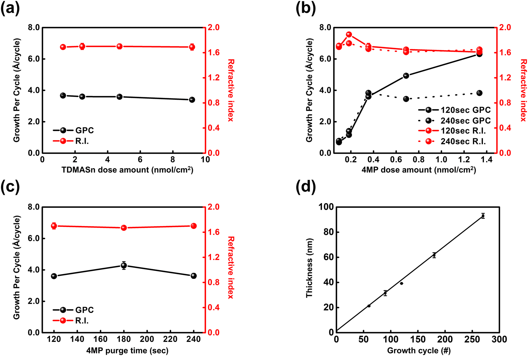 | ||
| Fig. 2 MLD process characteristics of tincone films. (a) GPC and refractive index as a function of TDMASn dose amount. (b) GPC and refractive index as a function of 4MP dose amount with different soak times (120 s and 240 s). (c) GPC and refractive index versus 4MP purge time. (d) Film thickness as a function of the number of growth cycles, showing linear growth behavior. | ||
To determine whether an insufficient purge time was the cause of the continuous increase in GPC, the deposition process was re-evaluated with an extended purge time of 240 s. The results indicated that the MLD curve reached saturation at a dose amount of 0.355 nmol cm−2 with a 240 s purge. Additionally, the GPC and refractive index for 120 and 240 s purges at 0.355 nmol cm−2 were comparable, which were measured at 3.6 Å per cycle and 1.7, respectively. To further verify this, the growth rate of the MLD tincone was analyzed across different purge times, as shown in Fig. 2(c). Although a slight increase in GPC was observed at 180 s, similar values for GPC and refractive index were observed for the 120 and 240 s purges. This indicates that a purge time longer than 120 s did not significantly affect the growth of the MLD tincone film at the tested dose amount. Therefore, a 120 s purge time was chosen for process efficiency. Based on these findings, we deposited all tincone films at a deposition temperature of 100 °C using the following process: dosing TDMASn for 1 s, purging with Ar for 30 s, dosing 4MP for 3 s, and completing the cycle with a 120 s Ar purge. This procedure maintained a linear growth behavior as the number of cycles increased, as shown in Fig. 2(d). The final GPC was determined by calculating the slope in Fig. 2(d), which yielded a value of 3.45 Å per cycle.
Previous studies on tincone materials have used organic linkers with hydroxyl functional groups, such as HQ, EG, and GL.16,17,22,23 Consequently, the elements constituting these tincones were limited to Sn, O, and C. However, in this study, we utilized 4MP, an organic linker containing S, leading to the presence of Sn, O, S, and C within the tincone film. Therefore, this study examined the impact of S, which differentiates our work from previous studies on tincone films. Fig. S3† shows the XPS survey, where peaks for Sn, O, S, and C were clearly identified, while no N 1s signal was detected in the 392–408 eV range. This absence of nitrogen, despite using a TDMASn precursor containing N, may indicate that nitrogen-based species were effectively removed during the MLD and annealing processes. Moreover, the distinct presence of Sn, S, O, and C peaks confirms that the spectral resolution and detection sensitivity were sufficient, reinforcing the interpretation that nitrogen-related impurities are below the detection limit and not incorporated into the film. Accordingly, the chemical bonding states of Sn, O, and S in the deposited tincone film were first investigated, as presented in Fig. 3. Curve fitting of the XPS spectra was performed to deconvolute each bond species. The XPS Sn 3d peak is shown in Fig. 3(a), where Sn is divided into Sn2+ (486.0 and 494.4 eV) and Sn4+ (486.7 and 495.1 eV).24–27 Despite using the Sn4+ precursor TDMASn, we observed a distribution of 49% Sn4+ and 51% Sn2+. Previous studies about tincone with divalent precursors have reported that both Sn2+ and Sn4+ can be observed owing to the incomplete reaction of organic reactants during the anticipated MLD reaction mechanism.17 Thus, the near-equal distribution of Sn4+ and Sn2+ indicates the possibility of incomplete reactions of the Sn molecules or incomplete elimination of precursor ligands, potentially due to low deposition temperature or imperfect reactions. In Fig. 3(b), the XPS O 1s peak reveals Sn–O (531.0 eV) and C–O (532.1 eV) bonding, with area concentrations of 62% and 38%, respectively.28–33 Consistent with the trends observed in previous metalcone studies, the Sn molecules of the metal precursor formed Sn–O bonds by reacting with the –OH groups on the substrate surface or with those present in the hydroxyl functional groups of the organic linker.28,29 In addition, the presence of C–O bonds in the 4MP organic linker was confirmed.34Fig. 3(c) shows the XPS S 2p spectrum, which was deconvoluted into contributions from Sn–S (162.3 eV) and C–S (163.0 eV) bonds.24,25 The spin–orbit splitting energy, defined as the energy difference between the S 2p3/2 and S 2p1/2 components, was determined to be 1.18 eV, which is consistent with reported values for sulfur-containing compounds.
 | ||
| Fig. 3 XPS spectra of (a) Sn 3d, (b) O 1s, and (c) S 2p for the as-deposited tincone film. The spectra were acquired using a Theta Probe ARXPS system (Thermo Fisher Scientific) with a monochromated Al Kα X-ray source (1486.6 eV), a spot size of 400 μm, a pass energy of 100 eV, a step size of 0.5 eV, and a dwell time of 100 ms over 50 scans. (d) Schematic of the proposed MLD mechanism for tincone film growth, based on the bonding states of Sn–O, Sn–S, C–O, and C–S identified via XPS. The illustration reflects the observed elemental composition, with Sn–O bonds shown approximately three times more frequently than Sn–S bonds. | ||
The area percentages of Sn–S and C–S bonds were approximately 64% and 36%, respectively. The presence of Sn–S bonds indicates that both the -OH and -SH functional groups in the 4MP reactant serve as reaction sites for the TDMASn precursor. Moreover, the linear growth of tincone during MLD cycles would not have occurred if the thiol group of 4MP did not participate as a reaction site. The proposed MLD mechanism for the formation of tincone films, based on the bonding states of Sn–O, Sn–S, C–O, and C–S present in the film, is illustrated in Fig. 3(d). The process begins with the adsorption of TDMASn onto the substrate surface, where the –OH and –SH functional groups coexist. The reaction produces HN(CH3)2 as a by-product, which is subsequently purged. The adsorbed TDMASn then reacts with 4MP, generating HN(CH3)2 as a byproduct and forming a monolayer of tincone on the surface. This cycle is repeated with the subsequent adsorption of TDMASn onto the 4MP layer, enabling the tincone films to grow linearly, as demonstrated in Fig. 2(d). To reflect the compositional ratio observed in XPS (Table 1), the schematic depicts Sn–O bonds approximately three times more frequently than Sn–S bonds, highlighting the dominant reactivity of –OH over –SH in this system. This mechanism is hypothetical and derived from ex situ characterization, rather than being directly confirmed through in situ analysis.
| As-dep. | 300 °C | 400 °C | 500 °C | 600 °C | |
|---|---|---|---|---|---|
| S (at%) | 6.30 | 7.40 | 6.83 | 4.22 | 3.80 |
| C (at%) | 67.3 | 65.2 | 71.1 | 82.7 | 85.4 |
| Sn (at%) | 5.40 | 6.00 | 3.37 | 1.58 | 0.75 |
| O (at%) | 21.0 | 21.4 | 18.7 | 11.5 | 10.8 |
Hybrid films deposited via MLD, such as alucone and indicone, undergo bond dissociation and structural rearrangements when subjected to high-temperature annealing.15–18,35,36 During this process, the structural properties of the films could be adjusted based on their elemental compositions and annealing temperatures. To investigate the effect of S on the structural rearrangement of tincone films during annealing, we conducted targeted annealing experiments. The properties of the MLD tincone films changed after 1 h of vacuum annealing in a tube furnace. As shown in Fig. 4, both the thickness and refractive index of the tincone films varied significantly. The films shrank and exhibited a notable decrease in thickness. According to previous studies on the vacuum annealing of other MLD metalcone films, O and metal atoms are removed together as the annealing temperature increases, leading to film densification.15,16,37 Additionally, structural rearrangements such as the graphitization of hydroquinoxy rings contribute to increased film density and thickness reduction. Previous research on MLD alucone films showed a thickness reduction of less than 10% at 300 °C under vacuum.35 The MLD tincone films also experienced a reduction in thickness owing to the graphitization of the benzene backbone. Notably, the tincone films showed a significant decrease, with a 30.3% reduction at 300 °C. This shrinkage continued, reaching 57.5% at 400 °C, 80.3% at 500 °C, and 90.9% at 600 °C, although the rate of reduction gradually decreased at higher temperatures.
 | ||
| Fig. 4 Thickness and refractive index of tincone films annealed at different temperatures, measured by spectroscopic ellipsometry. | ||
The refractive index of the as-deposited MLD tincone film was 1.80, which is similar to a previously reported value of 1.78.17 The refractive index increased from 1.80 to 1.97 as the annealing temperature increased to 400 °C, corresponding to the densification of the film.38 The refractive index increasing to 1.97 can also be attributed to the film's structure becoming more carbon-like. Materials such as graphite, graphene, and amorphous carbon (a-C), which are pure carbon materials, typically have refractive indices of approximately 2.3–2.7 owing to their dense structures.36,39 This interpretation is further supported by XRD analysis (Fig. S4†), which shows the appearance of a broad peak near 26° corresponding to the (002) reflection of graphitic carbon (JCPDS #75-1621), while no peaks related to SnO or SnO2 crystalline phases were detected. These results suggest that the increase in refractive index is not due to the formation of Sn-based oxides but rather to the graphitization and densification of the film. However, while the film densified and graphitic carbon formed, the trend of increasing refractive index reversed above 400 °C. The refractive index decreased at temperatures higher than 400 °C, dropping from 1.80 to 1.57, while the thickness continued to decrease. This decrease in the refractive index typically occurs in MLD metalcone films during annealing, where surface C are removed and surface oxidation occurs, resulting in the formation of an inorganic layer.40 However, as shown in Fig. S5† and Table 1, Sn continuously decreases, with the Sn atomic concentration nearing zero at an annealing temperature of 600 °C. In other study on tincone, Sn was entirely removed as the annealing temperature increased.16 Thus, rather than forming an SnO or SnO2 inorganic layer due to surface oxidation, the refractive index likely decreased for other reasons. Further analyses were conducted to investigate the cause of this low refractive index.
As shown in Table 1, films annealed at 300 °C displayed similar characteristics to those at room temperature. However, starting from 400 °C, the O content began to decrease with an increasing annealing temperature, ultimately dropping to 10.8%. Similarly, the Sn content also declined, reaching nearly zero (0.75%) at 600 °C, which aligns with trends observed in previous indicone and tincone studies.15,16,36 In contrast, the S content decreased with the temperature but did not completely disappear, remaining at 3.8% at 600 °C. This suggests that, unlike other reported metalcone films, the decrease in refractive index observed above 400 °C could be attributed to the differential reactivity in the presence of S. All XPS analyses were performed before sputtering to prevent damage to the tincone films, particularly to their organic components. To justify this approach, we evaluated the film's stability under ambient conditions (25 °C, 50% RH), and the results—presented in Fig. S6†—show negligible changes in GPC and R.I. over 1000 hours, confirming the surface stability of the before sputtering samples. To determine whether S influenced the bonding state within the annealed tincone films, various bonds in the high-resolution XPS C 1s and S 2p peaks of as-deposited, 400 °C, and 600 °C annealed samples were analyzed and shown in Fig. 5(a) and (b).
 | ||
| Fig. 5 XPS spectra of tincone films annealed at different temperatures. (a) C 1s spectra showing changes in the C–S and C–C bonding regions, with an inset highlighting the increased C–S signal after annealing. (b) S 2p spectra indicating a shift from Sn–S to C–S bonding with increasing annealing temperature. | ||
Fig. 5(a) shows the changes in the C 1s peaks of the as-deposited sample and the samples annealed at 400 °C and 600 °C, with all data calibrated using the C–C peak at 284.6 eV as a reference. The graph shape begins to change noticeably above approximately 285 eV, and the inset highlights the changes in the intensity of the C–S peak at 285.2 eV.19,41 The intensity of the C–S peak was measured as 0.500, 0.466, and 0.529 for the as-deposited, 400 °C, and 600 °C samples, respectively. Additionally, at 400 °C, a peak corresponding to C![[double bond, length as m-dash]](https://www.rsc.org/images/entities/char_e001.gif) O bonds at 287.6 eV was observed, which was absent at 600 °C. These results suggest that, starting at 400 °C, C–C bonds are replaced by C–S bonds, leading to the gradual disruption of the graphitic carbon structure.
O bonds at 287.6 eV was observed, which was absent at 600 °C. These results suggest that, starting at 400 °C, C–C bonds are replaced by C–S bonds, leading to the gradual disruption of the graphitic carbon structure.
To further investigate changes in the C–S peak, the S 2p peak in Fig. 5(b) was analyzed. The tincone films at different annealing temperatures show a shift from Sn–S at 162.3 eV to C–S at 163.0 eV. This shift indicates that as the annealing temperature increases, C–S bonds dominate over Sn–S bonds within the tincone film. This dominance of C–S bonding over Sn–S bonding suggests that S preferentially bonds with C rather than Sn, leading to the disruption of the graphitic carbon structure, which was primarily composed of C–C bonds. Although a shift toward C–S bonding is observed to some extent above 400 °C, the C 1s peak shows that, unlike at 600 °C, a peak at 287.6 eV corresponding to CO is present at 400 °C.
To further verify whether S atoms substitute for the C atom and break down graphitic carbon, Raman analysis was performed to confirm the graphitization of the MLD tincone thin films, as shown in Fig. 6. This technique specifically focuses on analyzing the binding and defect structures of graphite, graphene, and graphene oxide. The most prominent features in the Raman spectra of graphitic materials are the so-called D band at approximately 1350 cm−1 and the G band appearing at 1582 cm−1 (graphite).19,42–47 As illustrated in Fig. 6(a), the as-deposited tincone films exhibited no significant Raman spectra in the graphitic carbon region. However, after annealing up to 600 °C, distinct Raman bands emerged at 1350 cm−1 (D band) and 1587 cm−1 (G band), along with features between 2500–3000 cm−1, characteristic of graphitic carbon's overtone of the D band. The D band is typically associated with sp3 carbon and represents defects or disorder at the edges of graphitic structures, while the G band corresponds to the stretching mode of sp2 carbon atoms, indicating the formation of ordered sp2 carbon networks.47 The emergence of these bands suggests the onset of graphitization when the temperature exceeds 300 °C, with the most pronounced graphitization occurring at 400 °C, as shown in Fig. 6(b). However, at temperatures beyond 400 °C, the intensity of the G band decreases, indicating that the sp2 carbon network begins to degrade. This degradation is further supported by the loss of the 2500–3000 cm−1 band, which is a hallmark of sp2 carbon structures.19,42,43,47
 | ||
| Fig. 6 Raman analysis of tincone films annealed at different temperatures. (a) Raman spectra showing the evolution of D, G, and 2D bands with increasing annealing temperature. (b) G peak intensity as a function of annealing temperature, indicating increased graphitic ordering up to 400 °C followed by degradation. (c) ID/IG ratio showing an increase with temperature, suggesting higher defect density or S incorporation at elevated temperatures. | ||
The intensity ratio of the G-band to the D-band (ID/IG) is a crucial metric in carbon-based materials, often used to assess the relative contribution of sp2 to sp3 carbon atoms and the degree of order within the sp2-hybridized carbon network.19,35,42–45,47–51 As shown in Fig. 6(c), the ID/IG ratio increased as the annealing temperature increased. An increase in this ratio has two implications. First, this may indicate that graphitic carbon was successfully formed with larger domains of graphitic regions.19,35,43 Second, it could indicate increased disorder within the graphitic structure.48–50 Typically, the formation of a well-ordered graphitic structure results in a stronger G band (indicative of sp2 carbon) and a weaker D band (signifying fewer defects). However, contrary to the typical trend in which the intensity of the G band strengthens and the D band weakens with increasing annealing temperature, the MLD tincone films deposited with the 4MP organic reactant exhibited the following: the intensity of the D band increased while that of the G band decreased as the annealing temperature increased. Even when accounting for the reduced film thickness, a trend of increasing D band and decreasing G band suggests that S atom, introduced from the 4MP precursor, exerts a “hindering” effect on the graphitization process.49 This hindrance can be attributed to the formation of C–S bonds, as observed in the XPS S 2p analysis (Fig. 5). As the Sn atomic composition decreased owing to annealing, the S atoms originally bonded to Sn in the Sn–S bond transitioned to form C–S bonds. This transition disrupts the typical graphitization process by replacing the C–C and CC bonds necessary for the sp2 carbon network formation, thereby preventing the complete development of graphitic carbon domains. Based on the Raman spectral observations, the S atom in the 4MP organic reactant evidently hinders the formation of ordered sp2 carbon structures, leading to greater structural disorder at higher annealing temperatures.
With a decrease in the thickness of the tincone thin films and changes in the C binding due to annealing, the surface morphology and roughness also underwent significant alterations. The AFM results presented in Fig. 7 illustrate the changes in the roughness of the films and the breakdown of the sp2 carbon network, as evidenced by the 3D surface image of the film. Fig. 7(a) shows the as-deposited tincone film, where the surface roughness, previously reported to be approximately 0.18 nm, closely matches the roughness value of 0.186 nm measured in this study.22 Typically, the annealing of metalcones results in thickness reduction and densification, leading to a decrease in surface roughness.36 This trend was also observed in our experiments, where the roughness decreased with increasing annealing temperatures up to 400 °C. As shown in Fig. 7(b), the surface roughness of the film at 300 °C was 0.136 nm, which was significantly lower that of the as-deposited tincone film. Additionally, the RMS value at 400 °C depicted in Fig. 7(c) was 0.177 nm. This suggests that up to an annealing temperature of 400 °C, tincone films made with 4MP reactant successfully formed graphitic carbon like the other metalcone films did, resulting in a smoother surface. Meanwhile, in Fig. 7(d) and (e), the surface roughness exhibited an upward trend rather than a decrease at annealing temperatures of 500 and 600 °C. As the annealing temperature increased, the RMS value nearly doubled, reaching 0.377 nm at 500 °C and 0.855 nm at 600 °C. This phenomenon is presumed to result from the breakdown of sp2 carbon covalent bonds, coupled with the substitution of C atoms by larger S atoms. The covalent radius of S atom is 103 pm, whereas that of C atom is 77 pm, making S over 34% larger than C.52,53 The large substitutional atoms of C for S have been reported to alter the interlayer distance and modify the bond angles.54 This indicates that the presence of larger S atoms contributes to the observed increase in surface roughness. Additionally, although Sn is gradually removed from the film during annealing, as confirmed by XPS analysis, the comparison with other metalcone systems such as Indicone and Alucone suggests that metal removal alone is not the primary driver of roughness evolution. Therefore, the roughness increase is more reasonably attributed to structural deformation in the carbon framework induced by the incorporation of S, rather than by the absence of Sn.
 | ||
| Fig. 7 AFM images of tincone films annealed at different temperatures: (a) as-deposited, (b) 300 °C, (c) 400 °C, (d) 500 °C, and (e) 600 °C. RMS roughness initially decreases after mild annealing (up to 300 °C), then increases significantly above 400 °C, indicating thermally induced surface restructuring and potential sulfur-related effects. | ||
4. Conclusions
This study presents a detailed investigation of the graphitization of sulfur-containing tincone films synthesized via MLD using TDMASn as the metal precursor and 4MP as the organic linker. The vacuum post-annealing process at temperatures ranging from 300 to 600 °C revealed significant compositional and structural changes. Notably, at 400 °C, the film thickness decreased by 57.5%, and the refractive index increased from 1.8 to 1.97, indicating the successful formation of sp2 carbon. XPS analysis confirmed a reduction in residual Sn content to 0.75%. However, unique behavior was observed at temperatures exceeding 400 °C, where increased C–S bonding from the thiol (–SH) groups in 4MP disrupted the graphitic structure. This disruption results in decreased C–C bonding and a diminished G-band peak in the Raman spectra, highlighting the adverse impact of S substitution on the sp2 carbon network. These findings underscore the critical role of S in the structural stability of sp2 carbon films and emphasize the importance of carefully selecting metal precursors and organic linkers in MLD processes to optimize carbon film properties. This work lays a foundation for further research into fine-tuning the MLD parameters for enhanced performance in semiconductor and electronic applications.Author contributions
H. Jung and H. L. Yang contributed equally to this study. H. Jung and H. L. Yang collaborated in the fabrication of tincone films through MLD and co-authored the manuscript. G.B. Park and J.M. Kim contributed to the AFM analyses. H. Jung, H. L. Yang, and J.S. Park discussed and interpreted the significance of all experimental and analytical results in this study. All authors have given approval to the final version of the manuscript.Data availability
The data supporting this article have been included as part of the ESI.†Conflicts of interest
The authors declare that they have no known competing financial interests or personal relationships that could have appeared to influence the work reported in this paper.Acknowledgements
This work was supported by the Industry Technology R&D Program (20014639) funded By the Ministry of Trade, Industry & Energy (MOTIE, Korea) and National Research Foundation of Korea (NRF) grant funded by the Korea government (MSIT) (No. RS-2023-00260527). The XPS, Raman and AFM measurements were performed using instruments installed at the Hanyang LINC3.0 Analytical Equipment Center (Seoul).References
- Y. Wang, L. Zhang, H. Hou, W. Xu, G. Duan, S. He, K. Liu and S. Jiang, J. Mater. Sci., 2021, 56, 173–200 CAS.
- M. M. Sabzehmeidani, S. Mahnaee, M. Ghaedi, H. Heidari and V. A. L. Roy, Mater. Adv., 2021, 2, 598–627 CAS.
- P. R. Unwin, A. G. Güell and G. Zhang, Acc. Chem. Res., 2016, 49, 2041–2048 CAS.
- V. Meunier, A. G. Souza Filho, E. B. Barros and M. S. Dresselhaus, Rev. Mod. Phys., 2016, 88, 1–50 CrossRef.
- J. Lee, Y. Seo, S. Ban, D. G. Kim, Y. B. Park, T. H. Lee and H. Hwang, IEEE Trans. Electron Devices, 2024, 71, 3351–3357 CAS.
- H. J. Sung, M. Choi, Z. Wu, H. Chae, S. Heo, Y. Kang, B. Koo, J. B. Park, W. Yang, Y. Park, Y. Ham, K. Yang and C. S. Lee, Adv. Sci., 2024, 2408028, 1–11 Search PubMed.
- B. McBennett, Y. Esashi, N. W. Jenkins, A. Beardo, Y. Shao, E. E. Nelson, T. H. Culman, B. Abad, M. Tanksalvala, T. D. Frazer, S. Marks, W. Chao, S. Yazdi, J. L. Knobloch, H. C. Kapteyn and M. M. Murnane, Phys. Rev. Mater., 2024, 096001, 1–14 Search PubMed.
- H. Y. Liu, Z. Zhu, J. He, Y. Yang, Y. Liang, Z. Li, M. Zhu, M. Xiao and Z. Zhang, Nano Lett., 2024, 24, 10510–10518 CAS.
- Y. Liu, S. Ding, W. Li, Z. Zhang, Z. Pan, Y. Ze, B. Gao, Y. Zhang, C. Jin, L. M. Peng and Z. Zhang, ACS Nano, 2024, 18, 19086–19098 CAS.
- Y. M. Manawi, Ihsanullah, A. Samara, T. Al-Ansari and M. A. Atieh, Materials, 2018, 11, 822 Search PubMed.
- J. Multia and M. Karppinen, Adv. Mater. Interfaces, 2022, 9, 2200210 CAS.
- C. F. Herrmann, F. H. Fabreguette, D. S. Finch, R. Geiss and S. M. George, Appl. Phys. Lett., 2005, 87, 1–3 Search PubMed.
- Y. Lei, J. Lu, X. Luo, T. Wu, P. Du, X. Zhang, Y. Ren, J. Wen, D. J. Miller, J. T. Miller, Y. K. Sun, J. W. Elam and K. Amine, Nano Lett., 2013, 13, 4182–4189 CAS.
- L. M. Esteves, H. A. Oliveira and F. B. Passos, J. Ind. Eng. Chem., 2018, 65, 1–12 CAS.
- S. Lee, M. Kim, G. Baek, H. M. Kim, T. T. N. Van, D. Gwak, K. Heo, B. Shong and J. S. Park, ACS Appl. Mater. Interfaces, 2020, 12, 43212–43221 CAS.
- G. Baek, H. L. Yang, G. B. Park and J. S. Park, Jpn. J. Appl. Phys., 2023, 62, SG0810 CrossRef CAS.
- G. Baek, S. Lee, H. M. Kim, S. H. Choi and J. S. Park, Dalton Trans., 2022, 51, 1829–1837 RSC.
- S. Lee, H. M. Kim, G. H. Baek and J. S. Park, ACS Appl. Mater. Interfaces, 2021, 13, 60144–60153 CrossRef CAS PubMed.
- G. Baek, S. Lee, J.-H. Lee and J.-S. Park, J. Vac. Sci. Technol., A, 2020, 38, 023204 CrossRef.
- H. Jain and P. Poodt, Dalton Trans., 2021, 50, 5807–5818 RSC.
- A. Philip, L. Mai, R. Ghiyasi, A. Devi and M. Karppinen, Dalton Trans., 2022, 51, 14508–14516 RSC.
- K. Van de Kerckhove, J. Dendooven and C. Detavernier, J. Vac. Sci. Technol., A, 2018, 36, 051512 CrossRef.
- H. Zhu, M. H. A. Shiraz, L. Yao, K. Adair, Z. Wang, H. Tong, X. Song, T. K. Sham, M. Arjmand, X. Song and J. Liu, Chem. Commun., 2020, 56, 13221–13224 RSC.
- C. Chen, L. Xun, P. Zhang, J. Zhang and B. Tian, Res. Chem. Intermed., 2019, 45, 3513–3524 CrossRef CAS.
- Z. Zhang, C. Shao, X. Li, Y. Sun, M. Zhang, J. Mu, P. Zhang, Z. Guo and Y. Liu, Nanoscale, 2013, 5, 606–618 RSC.
- Z. Wang, D. Kong, M. Wang, G. Wang, N. Li and D. Li, RSC Adv., 2019, 9, 12990–12997 CAS.
- M. Li, X. Tian, S. Garg, T. E. Rufford, P. Zhao, Y. Wu, A. J. Yago, L. Ge, V. Rudolph and G. Wang, ACS Appl. Mater. Interfaces, 2020, 12, 22760–22770 CAS.
- J. Kint, F. Mattelaer, S. S. T. Vandenbroucke, A. Muriqi, M. M. Minjauw, M. Nisula, P. M. Vereecken, M. Nolan, J. Dendooven and C. Detavernier, Chem. Mater., 2020, 32, 4451–4466 Search PubMed.
- E. Kazyak, M. Shin, W. S. Lepage, T. H. Cho and N. P. Dasgupta, Chem. Commun., 2020, 56, 15537–15540 RSC.
- G. Yang, Y. Li, X. Wang, Z. Zhang, J. Huang, J. Zhang, X. Liang, J. Su, L. Ouyang and J. Huang, Nanomaterials, 2023, 13, 271 CrossRef CAS PubMed.
- D. Sassone, J. Zeng, M. Fontana, M. A. Farkhondehfal, C. F. Pirri and S. Bocchini, ACS Appl. Mater. Interfaces, 2022, 14, 42144–42152 CrossRef CAS PubMed.
- M. Kwoka, L. Ottaviano, M. Passacantando, S. Santucci, G. Czempik and J. Szuber, Thin Solid Films, 2005, 490, 36–42 CrossRef CAS.
- X. Feng, Z. Zhang, T. Zhang, J. Xue, C. Han, L. Dai, L. Wang and Z. He, Front. Chem., 2021, 9, 3–10 Search PubMed.
- H. Wang, K. E. Gregorczyk, S. B. Lee, G. W. Rubloff and C. F. Lin, J. Phys. Chem. C, 2020, 124, 6830–6837 CrossRef CAS.
- S. Lee, G. H. Baek, J. H. Lee, D. W. Choi, B. Shong and J. S. Park, Appl. Surf. Sci., 2018, 458, 864–871 CrossRef CAS.
- S. Lee, G. Baek, H. L. Yang, T. T. Ngoc Van, S. W. Kim, Y. K. Kim, B. Shong and J. S. Park, Adv. Mater. Interfaces, 2022, 9, 2201411 Search PubMed.
- A. I. Abdulagatov, R. A. Hall, J. L. Sutherland, B. H. Lee, A. S. Cavanagh and S. M. George, Chem. Mater., 2012, 24, 2854–2863 CAS.
- D. Mergel, D. Buschendorf, S. Eggert, R. Grammes and B. Samset, Thin Solid Films, 2000, 371, 218–224 CAS.
- X. Wang, Y. P. Chen and D. D. Nolte, Opt. Express, 2008, 16, 22105 CAS.
- B. H. Lee, B. Yoon, V. R. Anderson and S. M. George, J. Phys. Chem. C, 2012, 116, 3250–3257 CAS.
- J. Mei, J. Han, F. Wu, Q. Pan, F. Zheng, J. Jiang, Y. Huang, H. Wang, K. Liu and Q. Li, Front. Chem., 2023, 10, 1–10 RSC.
- L. G. Cançado, A. Jorio, E. H. M. Ferreira, F. Stavale, C. A. Achete, R. B. Capaz, M. V. O. Moutinho, A. Lombardo, T. S. Kulmala and A. C. Ferrari, Nano Lett., 2011, 11, 3190–3196 CrossRef PubMed.
- C. Y. Su, Y. Xu, W. Zhang, J. Zhao, X. Tang, C. H. Tsai and L. J. Li, Chem. Mater., 2009, 21, 5674–5680 CrossRef CAS.
- E. H. Martins Ferreira, M. V. O. Moutinho, F. Stavale, M. M. Lucchese, R. B. Capaz, C. A. Achete and A. Jorio, Phys. Rev. B, 2010, 82, 125429 CrossRef.
- L. M. Malard, M. A. Pimenta, G. Dresselhaus and M. S. Dresselhaus, Phys. Rep., 2009, 473, 51–87 CrossRef CAS.
- A. C. Ferrari, J. C. Meyer, V. Scardaci, C. Casiraghi, M. Lazzeri, F. Mauri, S. Piscanec, D. Jiang, K. S. Novoselov, S. Roth and A. K. Geim, Phys. Rev. Lett., 2006, 97, 1–4 Search PubMed.
- M. A. Pimenta, G. Dresselhaus, M. S. Dresselhaus, L. G. Cançado, A. Jorio and R. Saito, Phys. Chem. Chem. Phys., 2007, 9, 1276–1291 RSC.
- S. Stankovich, D. A. Dikin, R. D. Piner, K. A. Kohlhaas, A. Kleinhammes, Y. Jia, Y. Wu, S. B. T. Nguyen and R. S. Ruoff, Carbon, 2007, 45, 1558–1565 CrossRef CAS.
- R. Zhu, Q. Chen, X. Wang, S. Wang, J. Zhu and H. He, RSC Adv., 2015, 5, 7522–7528 RSC.
- J. I. Paredes, S. Villar-Rodil, P. Solís-Fernández, A. Martínez-Alonso and J. M. D. Tascón, Langmuir, 2009, 25, 5957–5968 CrossRef CAS PubMed.
- A. Reina, X. Jia, J. Ho, D. Nezich, H. Son, V. Bulovic, M. S. Dresselhaus and K. Jing, Nano Lett., 2009, 9, 30–35 CrossRef CAS PubMed.
- C. H. Suresh and N. Koga, J. Phys. Chem. A, 2001, 105, 5940–5944 CAS.
- H. Paulsen, Angew. Chem., Int. Ed. Engl., 1982, 21, 155–173 Search PubMed.
- G. Ma, G. Ning and Q. Wei, Carbon, 2022, 195, 328–340 CrossRef CAS.
Footnotes |
| † Electronic supplementary information (ESI) available. See DOI: https://doi.org/10.1039/d5dt00529a |
| ‡ These authors contributed equally to this work. |
| This journal is © The Royal Society of Chemistry 2025 |