
Probing the significance of phenylethyl ammonium doping in Cs3Bi2Br9 halide perovskite nanosheets: a structural and optical perspective†
Fency
Sunny
a,
Priyakumari
Chakkingal Parambil
b,
Nandakumar
Kalarikkal
 *acd and
Kurukkal Balakrishnan
Subila
*e
*acd and
Kurukkal Balakrishnan
Subila
*e
aInternational and Inter University Centre for Nanoscience and Nanotechnology, Mahatma Gandhi University, Kottayam 686 560, Kerala, India
bDepartment of Chemical Sciences, Indian Institute of Science Education and Research Mohali, India
cSchool of Pure and Applied Physics, Mahatma Gandhi University, Kottayam 686 560, Kerala, India
dInternational Centre for Ultrafast Studies, Mahatma Gandhi University, Kottayam 686 560, Kerala, India. E-mail: nkkalarikkal@mgu.ac.in
eSchool of Chemical Sciences, Mahatma Gandhi University, Kottayam 686 560, Kerala, India. E-mail: subilakb@gmail.com
First published on 8th April 2025
Abstract
Lead-free halide perovskites have been explored ardently for optoelectronic applications. Organic–inorganic hybrid halide perovskites have shown promise with novel optical properties, bandgap tuning and improved carrier dynamics, while introducing a quantum well structure. Herein, phenylethyl ammonium (PEA), an organic cation, was incorporated into cesium bismuth bromide (CBB) to enhance its multi-quantum well structure and synthesize organic–inorganic hybrid nanosheets of PEA-doped cesium bismuth bromide (PEA:CBB). Optimal doping conditions led to the formation of stable layered PEA:CBB hybrid nanosheets, evidenced by XRD and HRTEM analyses. DFT calculations revealed a minimum-energy structure in which PEA adopts a horizontal alignment between the inorganic slabs of CBB. The incorporation of PEA introduces new electronic states, resulting in extended luminescence tails and altered carrier lifetime. Third-order non-linear optical characterization of pristine and hybrid particles revealed that the multi-quantum well structure and additional trap states induced by PEA increase the two-photon absorption coefficient and reduce the optical limiting threshold of CBB. The present study indicates conceivable relevance of lead-free bismuth-based halide perovskites and their variants in optical limiting applications.
1. Introduction
Halide perovskites have garnered significant attention in the optoelectronic field owing to their excellent optical properties and tunable bandgaps. Their inherent versatility to autonomously and synergistically form hybrid structures by amalgamating organic and inorganic components enables effective modulation of structural, optical, and electronic properties. Though research on halide perovskites initially focused on lead-based systems, concerns over lead toxicity and their instability under heat, air and moisture has opened up a new avenue for research on its lead-free alternatives.1–3 Most studies on lead-free perovskites have focused on the replacement of Pb with Sn, Bi, Ge, and Sb due to their similar electronic configurations.4–9 In particular, Bi- and Sb-based A3B2X9 perovskites (where B = Bi or Sb) have emerged as promising greener and more stable candidates.10 These perovskites are composed of corner-sharing double-layered [BBr6]3− octahedra, with one-third of the B cation sites unoccupied compared to conventional ABX3 perovskites. While several studies have explored the phase, crystal structure and optical properties of bismuth-based perovskites, only a few have reported their optoelectronic and photovoltaic applications.11–13 A more detailed investigation of these greener and less toxic perovskites is necessary to better understand their properties and identify practical applications.Tuning optical properties has been the foremost motivation for cation or anion engineering in lead-based halide perovskites. Varying anions and/or A-site cations in Pb-based perovskites has enabled the tuning of bandgaps across the entire visible spectrum.14 Organic molecules have been observed to occupy the A-site cation, enhancing the electrostatic stability of perovskites without considerably affecting their electronic structure. However, the incorporation of organic cations can reduce structural symmetry, which may alter the electronic states of the perovskites.15 Moreover, introducing organic molecules that interact strongly with the inorganic framework allows effective modulation of optoelectronic properties.16 Organic cations such as phenylethyl ammonium (PEA) or butylammonium(BA) are known to occupy the spaces between the inorganic layers of corner-sharing [BX6] octahedra, acting as spacer cations and resulting in layered halide perovskites structures. These structures exhibit enhanced stability owing to the bulky and hydrophobic nature of the organic molecules, and have been applied in photovoltaics and light-emitting diode applications.17–20 The incorporation of such organic molecules with large dielectric constants gives rise to intrinsic quantum-well (QW) structures, in which the semiconducting inorganic slabs act as the quantum wells and the organic dielectric layers serve as barriers.21 This architecture leads to interesting optical and electronic properties applicable in different optoelectronic devices.
Along with linear optical properties, nonlinear optics has been a focus in 3D bulk semiconductor materials. However, with the dawn of 2D materials, systems including transition metal dichalcogenides (TMDs) (WS2, WSe2, MoS2, MoSe2etc.), black phosphorus (BP), hexagonal boron nitride (h-BN), and halide perovskites have shown promising non-linear properties that expand their technological relevance.22 2D materials find successful application in non-linear technology due to their large and ultrafast nonlinear optical response, broadband and tunable optical absorption, ultrafast recovery time, considerable optical and thermal damage thresholds, high chemical and mechanical stability, and inexpensive fabrication methods. The strong optical nonlinearity and ultrafast response of these materials have been successfully employed in all-optical modulators, saturable absorbers (SAbs) used in passive mode locking and Q-switching, wavelength converters, and optical limiters.22
In perovskite structures, introducing dopant cations has proved to change carrier type and mobility, along with the band structure. Incorporation of an organic cation such as phenylethylammonium (PEA) or butylammonium (BA) has been shown to increase stability and form layered perovskites with intriguing properties. Addition of an organic cation could also enhance the nonlinear absorption coefficient, attributed to the enhanced quantum and dielectric confinement in the organic–inorganic multi-quantum-well structure.23 In this work, we have designed a simple and straightforward method for synthesising PEA-doped Cs3Bi2Br9 nanosheets to tune the multi-quantum well structure of Cs3Bi2Br9, employing a single-step one-pot heating up method. The structural, morphological and optical characterisation of the samples was carried out to analyse the changes promoted by PEA addition. The non-linear characteristics of the samples were analysed using open-aperture Z-scan method. The systematic studies showed that PEA incorporations tunes the optical properties of Cs3Bi2Br9. The investigations demonstrated that PEA-doped Cs3Bi2Br9 shows potential in optical limiter applications.
2. Results and discussion
A modified heating-up method, as described in the experimental methods section, was followed for the synthesis of pristine and PEA-doped Cs3Bi2Br9 (CBB). The fundamental characterizations were performed via X-ray diffraction, Raman spectroscopy and high-resolution transmission electron microscopy.The phase and crystal structures of PEA-doped CBB were investigated via X-ray diffraction (XRD) studies. Fig. 1(a) shows the XRD patterns of pristine and PEA-doped CBB perovskites. CBB shows five prominent diffraction peaks originating from the (001), (101), (110), (003) and (022) planes, which match well with standard ICSD data (ICSD: 01-070-0493), as shown in Fig. 1(a) (black trace). This confirms that the synthesised CBB adopts a hexagonal crystal lattice with the space group P![[3 with combining macron]](https://www.rsc.org/images/entities/char_0033_0304.gif) m1. At room temperature, CBB consists of bilayers of Bi3+ octahedra lying perpendicular to the crystallographic c-axis (Fig. 2(a)). In the XRD reflections, peaks corresponding to planes lying fully parallel to the c-axis, including the (001), (002) and (003) planes, are relatively sharp and exhibit smaller FWHM values compared to the reflections corresponding to planes with components perpendicular to the c-axis. This indicates a smaller dimension in this direction. This anisotropy is also observed in the TEM images, which reveal that the sample consists of small nanoplatelets with lateral dimensions of approximately 150 nm. The lattice parameters of the hexagonal lattice of CBB were calculated using the equation
m1. At room temperature, CBB consists of bilayers of Bi3+ octahedra lying perpendicular to the crystallographic c-axis (Fig. 2(a)). In the XRD reflections, peaks corresponding to planes lying fully parallel to the c-axis, including the (001), (002) and (003) planes, are relatively sharp and exhibit smaller FWHM values compared to the reflections corresponding to planes with components perpendicular to the c-axis. This indicates a smaller dimension in this direction. This anisotropy is also observed in the TEM images, which reveal that the sample consists of small nanoplatelets with lateral dimensions of approximately 150 nm. The lattice parameters of the hexagonal lattice of CBB were calculated using the equation  as a = b = 7.98 ± 0.03 Å and c = 9.85 ± 0.05 Å.24
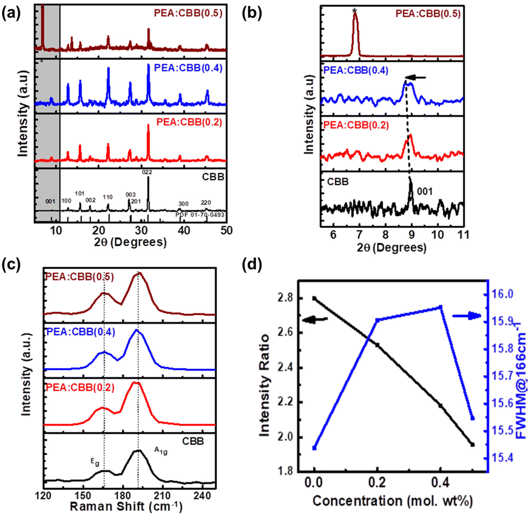 | ||
| Fig. 1 Structural Analysis of CBB and PEA:CBB. (a) XRD reflections of the pure and doped samples-CBB, PEA:CBB(0.2), PEA:CBB(0.4) and PEA:CBB(0.5), respectively. The doped samples show a relative shift in the diffraction angle of (001) plane towards lower angles (highlighted). (b) XRD reflections below 10°, clearly showing the (001) plane shifting from 8.9° to 8.6° in PEA:CBB(0.4) and the emergence of a new peak at 6.8° in PEA:CBB(0.5), indicating the formation of a secondary phase. (c) Raman spectra of the pure and doped samples-CBB, PEA:CBB(0.2), PEA:CBB(0.4) and PEA:CBB(0.5), respectively. (d) Variation in the intensity ratio and FWHM of the Raman peak at 166 cm−1, corresponding to the Eg resonance, as a function of dopant concentration. | ||
 | ||
| Fig. 2 Relaxed structures. DFT-optimized structures of (a) pristine CBB and (b) PEA-doped CBB. In the PEA:CBB structure, the phenyl ring of the PEA is oriented parallel to the inorganic layer. | ||
In accordance with Bragg's equation, if the spacing between crystal planes increases, the value of 2θ corresponding to the peak of the associated crystal plane will decrease. Upon doping with PEA, the (001) peak is observed to shift slightly towards a lower angle. The hexagonal phase of CBB encompasses a layered structure, wherein the inorganic sheets of cesium bismuth bromide alternate with layers of vacant space, hence the term vacancy-ordered perovskites. The shift and broadening of the (001) plane suggest the possible incorporation of PEA between the inorganic sheets. As the concentration of PEA dopant increases, a prominent peak at 6.8° corresponding to phenylethylammonium bismuth bromide (Fig. 1(a) and (b), marked with an asterisk), appears alongside the diffraction peaks of CBB.25 The formation of this new phase indicates the doping limit of PEA in CBB, and thus further doping was not pursued. Additionally, at the highest concentration, in the sample PEA:CBB(0.5), a peak at 32.5°, corresponding to the formation of bismuth oxybromide, is present as an impurity phase, indicating sample instability at high PEA concentrations. XRD reflections can also be employed to determine the extent of coherently diffracting domains. The crystallite size (D) was calculated using the Scherrer equation, given by  , where k is the shape factor (typically 0.94), λ is the wavelength of the incident X-ray, βD is the full width at half maximum of the most intense peak, and θ is the corresponding Bragg angle.13,26 The average crystallite size is observed to decrease slightly, from 38.44 nm in the pristine sample to 33.3 nm with increasing PEA concentration.
The structural variation induced by PEA doping was further analysed using Raman spectroscopy, under 532 nm excitation. Cs3Bi2Br9 exhibits two characteristic Raman peaks at 166 cm−1 and 191 cm−1, corresponding to the Eg and A1g modes, respectively.27,28 The Eg mode is attributed to the in-plane vibrational motion, whereas the A1g mode corresponds to the out-of-plane vibration of the [BiBr6]3− octahedron. As shown in Fig. 1(d), the FWHM of the Eg resonance increases with increasing the PEA content, indicating a reduced phonon lifetime. However, in the case of PEA:CBB(0.5), the FWHM decreases owing to the formation of the new phase that disrupts the regular lattice vibrations of CBB. Additionally, the intensity profile of the two vibrational peaks varies markedly with increasing dopant concentration (Fig. 1(d)). In particular, the of A1g![[thin space (1/6-em)]](https://www.rsc.org/images/entities/char_2009.gif) :Eg peak intensity ration decreases from 2.8 to 1.93 as the PEA content increases from 0 to 0.5 mol%. This suggests a relative suppression of the out-of-plane vibrations compared to the in-plane vibration. The enhancement of the Eg peak PEA incorporation supports the hypothesis that the aromatic ring of PEA intercalates between the planar CBB slabs, as inferred from XRD analysis, thereby restricting out-of-plane vibrations. Consequently, the observed decrease in the A1g:Eg intensity ratio further confirms the influence of PEA on the vibrational dynamics of the perovskite structure.
:Eg peak intensity ration decreases from 2.8 to 1.93 as the PEA content increases from 0 to 0.5 mol%. This suggests a relative suppression of the out-of-plane vibrations compared to the in-plane vibration. The enhancement of the Eg peak PEA incorporation supports the hypothesis that the aromatic ring of PEA intercalates between the planar CBB slabs, as inferred from XRD analysis, thereby restricting out-of-plane vibrations. Consequently, the observed decrease in the A1g:Eg intensity ratio further confirms the influence of PEA on the vibrational dynamics of the perovskite structure.
Based on the inferences drawn from XRD and Raman spectroscopy, DFT calculations were performed to elucidate the stable structure in the PEA-incorporated system. Doping with PEA can occur by replacing either the surface Cs atoms (those located at the top and bottom of the Bi2Br9 layer), the central Cs atoms, or both. However, surface doping is more likely than central doping, as the former does not disturb the network of [BiBr6]3− octahedra. The surface-doped structure (Fig. 2(b)) is more stable by 0.97 eV per cell. Among the various possible orientations of PEA, the configuration in which the phenyl ring lies parallel to the inorganic layer is found to be the most stable, possibly due to favorable interactions between Cs+ ions and the π system of the phenyl ring. The presence of the ammonium ion and the phenyl ring in PEA-doped samples was confirmed via FTIR and XPS analyses. FTIR spectra confirmed the presence of N–H out-of-plane vibrations and N–H stretching vibrations, along with aromatic C–H stretching modes in PEA:CBB (Fig. S2†). XPS analysis was further employed to understand the variation in N 1s peak upon PEA doping. A shift towards higher binding energy was observed with PEA addition, indicating a change in the chemical environment of N 1s (Fig. S3b†). In pristine CBB, the N 1s peak centred at 399 eV corresponds to the nitrogen in the amine group used as ligands during perovskite synthesis. Upon PEA incorporation, the presence of ammonium cations leads to the formation of an N 1s peak centred at 401 eV, further confirming the successful incorporation of PEA into the CBB lattice. The full XPS survey spectra are given in Fig. S3(a).† Elemental composition was further confirmed by EDX analysis (Fig. S4†), which verified the presence of Cs, Bi and Br in pristine and doped samples, along with a conspicuous presence of carbon in the PEA-doped material.
The morphology of the pristine, PEA:CBB(0.4) and PEA:CBB(0.5) samples was analysed using HRTEM imaging. The images showed the formation of nanoplatelets in CBB with an average edge length of 150 nm (Fig. 3(a)). On doping with PEA, the nanoplatelets were seen to grow in size, with the average edge length of the nanosheets found to be around 200 nm (Fig. 3(b)). In PEA:CBB(0.5), however, the average length increased to 250 nm, with the platelets growing in dimension to about 750 nm, resulting in nanosheets (Fig. 3(c) and S5†). This sheds light on the impact of addition an A-site cation substitute in cesium bismuth bromide. The systemic addition of varying amounts of PEA leads to gradual growth of the nanoplatelets. This signifies that, just as in cesium lead bromide perovskites, perovskite growth can be tuned via the nature of the A-site cations in CBB as well. The HRTEM images and the SAED patterns confirm the high crystallinity of the samples. PEA:CBB(0.4) and PEA:CBB(0.5) are seen to be substantially more crystalline than CBB. The lattice fringes shown in Fig. 3(d)–(f) with a d-spacing of 0.39 nm corresponds to the (110) plane.
 | ||
| Fig. 3 Morphological analysis of CBB and PEA:CBB. TEM images (a), (b) and (c); HRTEM images (d), (e), and (f); and corresponding SAED pattern (insets) of CBB, PEA:CBB(0.4) and PEA:CBB(0.5), respectively. The HRTEM images (d), (e) and (f) reveal the prominent lattice fringes with a d-spacing of 0.39 nm, corresponding to the (110) plane. The SAED patterns shown in the insets of (d), (e) and (f) confirm the crystallinity of the nanoparticles, which increases with the dopant PEA. | ||
In the electronic structure of Cs3Bi2Br9 perovskites, the valence-band (VB) maximum consists mainly of a mixture of bromide p and bismuth 6s orbitals, whereas the conduction-band (CB) minimum originates primarily from the bismuth 6p orbitals. This gives the band-edge transition a mix of charge-transfer and bismuth 6s–6p characteristics (Fig. S1†).29 The absorption spectra of the Cs3Bi2Br9 nanoplatelets are generally similar to those reported for bulk crystals and thin films, centred at 436 nm, as shown in Fig. 4(a) (black trace). The charge carriers exhibit large effective masses and a resulting limited delocalization in these materials.24,29,30 Introducing PEA leads to a slight redshift of the absorbance peak from 436 to 442 nm. As the amount of dopant increases, the shift of the absorbance peak to longer wavelength is attributed to the increase in the dimensions of the nanoparticles, as they change from thin platelets to sheets, as evidenced in the TEM images. The indirect bandgap of the pure and doped samples was calculated using Tauc plots (Fig. 4(b)). CBB exhibits an indirect bandgap of 2.48 eV, which decreases to 2.41 eV in PEA:CBB(0.5) with increasing PEA content. This is indicative of the effect of dimensional growth due to PEA incorporation on the optical characteristics of CBB. The stability of the pristine and doped samples was also explored through absorbance spectral analysis. The samples were kept in ambient conditions, with humidity fluctuating between 72% and 90% for a period of six months. The absorbance spectra showed no prominent changes in this duration and exposure, indicating good moisture tolerance of the samples (Fig. S6†).
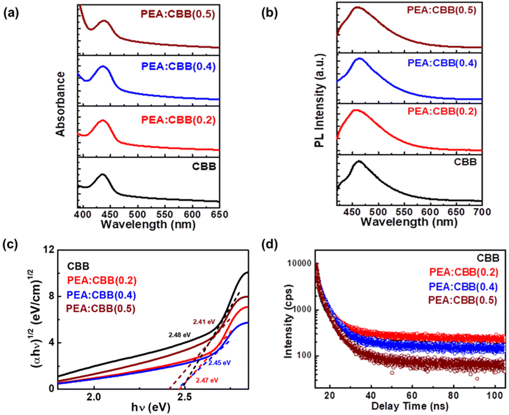 | ||
| Fig. 4 Photophysical characterization of CBB and PEA:CBB (a) UV-Vis absorbance spectra of the pristine and doped samples-CBB, PEA:CBB(0.2), PEA:CBB(0.4) and PEA:CBB(0.5), respectively. (b) Tauc plots for indirect band gaps of pure and doped samples-CBB, PEA:CBB(0.2), PEA:CBB(0.4) and PEA:CBB(0.5), respectively, showing a decrease in band gap from 2.48 eV in CBB to 2.41 eV in PEA:CBB(0.5). (c) Normalized photoluminescence spectra of the pristine and doped samples-CBB, PEA:CBB(0.2), PEA:CBB(0.4) and PEA:CBB(0.5), respectively. (d) Time-correlated single-photon counting measurements of the pristine and doped samples-CBB, PEA:CBB(0.2), PEA:CBB(0.4) and PEA:CBB(0.5), respectively, at 330 nm excitation. | ||
Weak photoluminescence (PL) has been observed in bulk CBB in some instances, in contrast to the bright blue emission seen in colloidal samples, wherein the origin of luminescence had remained unclear.31–33 This has been attributed to the residual unreacted precursors present in the nanocrystal samples.24,33,34 Proper purification has been shown to considerably reduce photoluminescence. The PL spectrum of CBB synthesised in this work reveals a single peak centred at 464 nm with a long tail (Fig. 4(b)), which correlates with the distinctive nature of CBB photoluminescence described earlier.35–37 Upon PEA incorporation, a slight red shift of 2 nm is observed in the emission peak. The FWHM of the PL peak increases with increasing PEA content, indicating an increased density of defect states. Thus the incorporation of PEA introduces additional defect states and, together with the increased nanosheet dimensions, ultimately leads to the increased FWHM in PEA:CBB.
Time-correlated single-photon counting analysis was performed on the pristine and doped CBB samples at the emission peak of 464 nm to quantify their emission lifetimes (Fig. 4(d)). The decay profiles were fitted using a triexponential function (Table S1†), with each component representing ultrafast (τ1), intermediate (τ2) and long-lived (τ3) carrier recombination processes. These components correspond to different carrier dynamics in CBB such as trap-assisted, excitonic and free carrier recombination (τ1, τ2 and τ3) processes. In pristine and PEA-doped CBB, the ultrafast and intermediate components dominate the decay profile (>80%), with excitonic recombination supported by the presence of a long emission tail in the PL peak.38 PEA incorporation results in an increase in the average PL lifetime with a greater contribution from the free charge carrier recombination and enhanced excitonic behaviour (Table S1†). As the nanoplatelets increase in dimension upon PEA doping, the newly introduced shallow defect states may temporarily trap charge carriers, followed by delayed recombination, leading to an extended average lifetime.39
For non-linear optical characterization, open-aperture (OA) Z-scan measurements were performed using a frequency-doubled Nd:YAG laser emitting 8 ns pulses at 532 nm. Compared to 3D perovskite structures, the incorporation of larger and more complex organic molecules results in structures that exceeded the Goldschmidt tolerance factor, making them more versatile and dynamic. Vacancy-ordered CBB perovskites inherently exhibit a multi-quantum well structure owing to the alternating layers of vacant position and CBB slabs.40 Incorporation of the organic molecule creates alternation between small bandgap inorganic semiconductors and large bandgap organic insulators, forming organic–inorganic multi-quantum well structures. This enhances quantum and dielectric confinement effects, which largely influence the two-photon absorption process. Thus, PEA-doped CBB shows a higher non-linear absorption than pristine CBB (Fig. 5(a–d), insets), with increasing input intensity attributed to an effective two-photon absorption (TPA) process, possibly accompanied by excited-state absorption (ESA) due to the presence of trap states.41 The intensity-dependent transmittance in such systems is described by the eqn (1):42
 | (1) |
 , and β is the effective TPA coefficient.
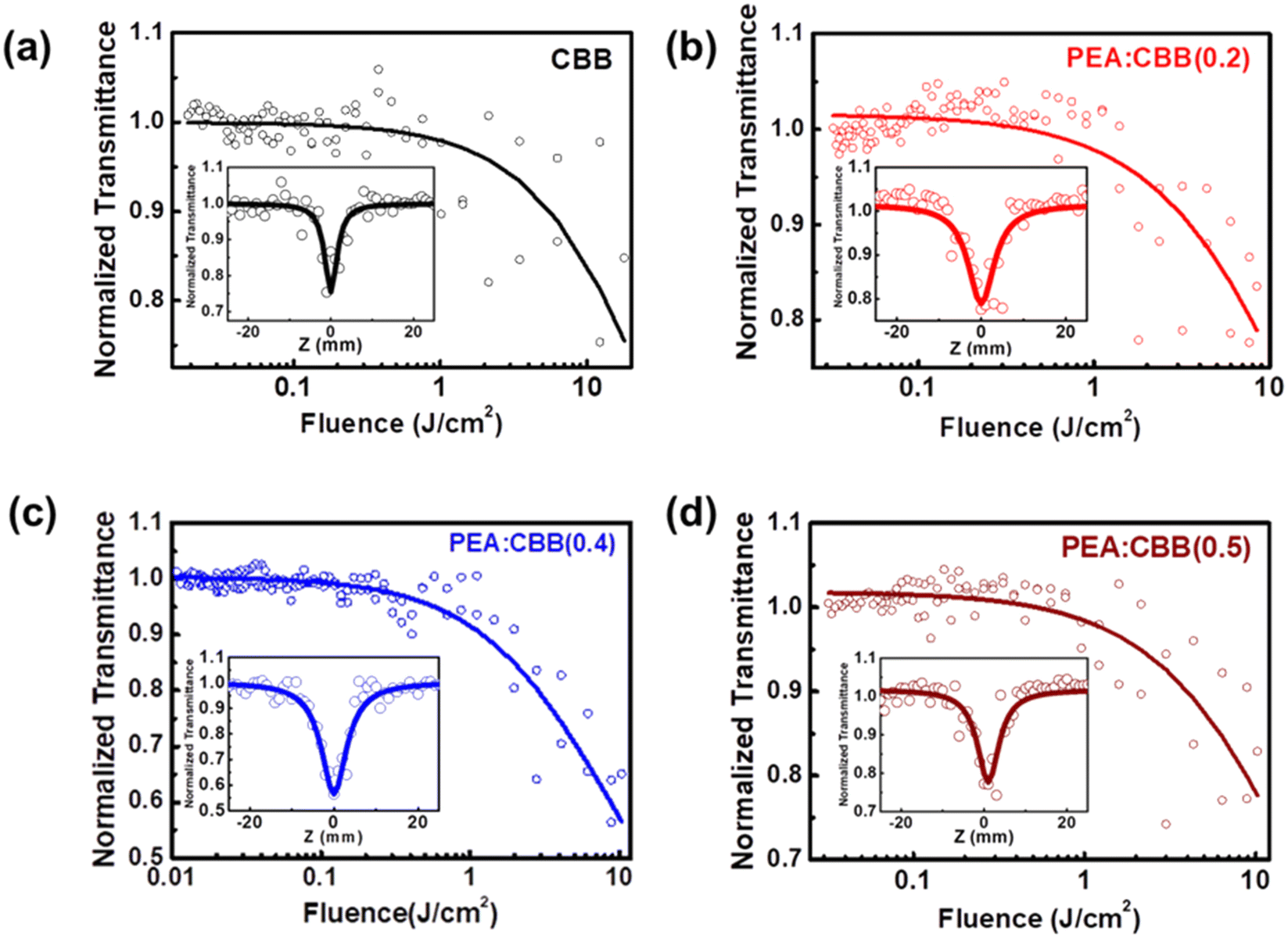 | ||
| Fig. 5 Open aperture Z-scan measurement and optical limiting behaviour. Fluence-dependent optical transmission of (a) CBB, (b) PEA:CBB(0.2), (c) PEA:CBB(0.4) and (d) PEA:CBB(0.5) samples, calculated from the OA Z-scan curves measured using 532 nm, 8 ns laser pulses with an average energy of 68 μJ per pulses. The normalized transmittance curves of (a) CBB, (b) PEA:CBB(0.2), (c) PEA:CBB(0.4) and (d) PEA:CBB(0.5) samples are provided in the insets. | ||
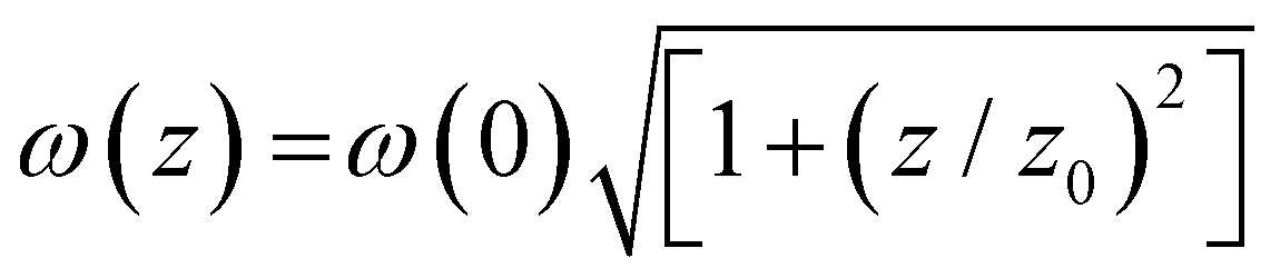
For a spatially Gaussian laser beam, each z position corresponds to an input laser energy density (fluence), which is given by eqn (2):
 | (2) |
 | (3) |
Using the equation, the two-photon absorption coefficient was calculated and the values are provided in Table S2.† The value of β is observed to increase with increasing PEA content. Specifically, the coefficient rises from 0.6101 GW cm−2 in pristine CBB to 2.532 GW cm−2 in PEA:CBB(0.4). However, upon increasing the PEA concentration, a decline in β is observed in PEA:CBB(0.5). This reduction is attributed to samples instability and the formation of impurity phases in PEA:CBB(0.5), as evidenced by the XRD analysis.
The projected density of states of pristine CBB and PEA:CBB provides insight into the possible origin of TPA. The density of states clearly shows the presence of states contributed by Bi p and Br p states at about 4.7 eV from the valence band. This indicates the feasibility of TPA under 532 nm excitation (Fig. 6(a)). It is evident that doping with PEA does not cause significant changes to the overall electronic structure. The density of states near the Fermi level remains unaltered. The carbon p orbitals contribute to states well below the valence band maximum and above the conduction band minimum. As PEA is incorporated into CBB, new C p states emerge in proximity to the Bi p and Br p states (Fig. 6(b), marked by an asterisk), thereby increasing the probability of two-photon absorption. This is observed as an increase in the experimentally calculated β values.
 | ||
| Fig. 6 Projected density of states of pristine CBB (a) and PEA:CBB (b) from DFT analysis. The new state formed from C p orbitals in the conduction band upon PEA addition is marked with an asterisk. | ||
The observations from the Z-scan can be further analysed to understand the optical limiting behaviour of the material. The optical limiting threshold value indicates the input fluence beyond which the material becomes opaque to incident radiation. A good optical limiter should have a lower threshold value. Halide perovskites have been studied as optical limiting materials, as they absorb the most intense laser light once the TPA threshold is reached.43,44 As the dopant concentration increases, the optical limiting threshold value is seen to be almost half of that for pure CBB (Fig. 5a–d). The lowering of the threshold implies that PEA-incorporated CBB nanosheets can be used as potential optical limiters for protection from laser damage.
3. Conclusions
We have successfully synthesised, for the first time, layered PEA-doped Cs3Bi2Br9 nanosheets. The structural and morphological variations were investigated by systemically increasing the amount of PEA. The XRD reflections showed a shift and broadening of the (001) plane, indicating the incorporation of PEA between inorganic layers. This was further confirmed via Raman spectroscopy, HRTEM analysis and DFT calculations. The stable structure of PEA-doped CBB was elucidated through DFT analysis, wherein the horizontally configured PEA was embedded between inorganic slabs of CBB. The PEA-induced growth of nanoplatelets into layered nanosheets was explicitly observed in TEM images. The UV-Vis absorbance spectra exhibited a slight shift in the absorbance peak and bandgap to lower energy, indicating the effect of nanoplatelet growth in CBB upon doping with PEA. The linear and non-linear optical characterisations of the material were methodically performed. The non-linear characterisation via Z-scan showed an increase in the two-photon absorption coefficient and a decrease in the optical limiting threshold with increasing PEA content. This study reveals that the successful incorporation of organic cations can be developed as a means for tuning the multi-quantum well properties of lead-free bismuth halide perovskites, pointing to novel applications in optoelectronics.Author contributions
Fency Sunny: conceptualization, formal analysis, visualization writing – original draft. Priyakumari Chakkingal Parambil: software, analysis, and resources. Nandakumar Kalarikkal: supervision, resources, and writing – editing and Subila Kurukkul Balakrishnan: supervision, validation, resources, and writing – editing.Data availability
The data supporting the findings of this article are included in the ESI.†Conflicts of interest
There are no conflicts of interest to declare.Acknowledgements
The authors acknowledge Dr Mallikarjun A and Mr Swalihu P.M. for conducting open aperture Z scan experiment. The author NK would like to acknowledge the financial support received from the CRS program of UGC-DAE CSR, Kolkata Centre (UGC-DAE-CSR-KC/CRS/19/RC08/0485), India, SERB: CRG (Grant No. CRG/2021/001506), UGC-Govt. of India for providing funding via the Innovative Program and Special Assistance Program (SAP Grant No. F.530/12/DRS/2009; F.530/13/DRS II/2016), RUSA, UGC: Scheme for Promotion of Academic and Research Collaboration (SPARC Grant No. P930, P1400, P1429, and P1460), DST: Nano Mission (Grant No. SR/NM/NS-1420-2014(C) and SR/NM/NS-54/2009), DST: Fund for Improvement of S&T Infrastructure (FIST Grant No. SR/FST/P SI-143/2009), DAE-Board of Research in Nuclear Sciences (BRNS Grant No. 39/29/2015-BRNS/39009), and DST Promotion of University Research and Scientific Excellence (PURSE Grant No. SR/S9/Z-23/2010/22(C, G)), Government of India programs for providing the facilities for research and development in IIUCNN, MGU. SKB acknowledges the DST, Government of India for the DST-SERB (EEQ/2023/000374) funding for the project entitled “Design and development of low-cost synthetic strategies and investigation of defect tolerance properties for Inorganic semiconductors for semiconductor sensitized solar cell applications“. The author FS is grateful to Mahatma Gandhi University, Kerala, India, for providing University JRF. The authors express gratitude to IIUCNN, MGU for the HRTEM imaging. We thank the facilities provided by SAIF, M G University and ISTEM facility for TCSPC studies and IIUCNN, M G University for XRD analysis. The authors SKB and FS thank the analysis facilities provided by SCS, M G University. PCP thanks the Indian Institute of Science Education and Research Mohali for the computational facility. The authors thank Ms. Shilpa Santhosh for her assistance in article proofreading.References
- J. Zhuang, J. Wang and F. Yan, Review on Chemical Stability of Lead Halide Perovskite Solar Cells, Nano-Micro Lett., 2023, 15(1), 84, DOI:10.1007/s40820-023-01046-0.
- A. F. Akbulatov, S. Y. Luchkin, L. A. Frolova, N. N. Dremova, K. L. Gerasimov, I. S. Zhidkov, D. V. Anokhin, E. Z. Kurmaev, K. J. Stevenson and P. A. Troshin, Probing the Intrinsic Thermal and Photochemical Stability of Hybrid and Inorganic Lead Halide Perovskites, J. Phys. Chem. Lett., 2017, 8(6), 1211–1218, DOI:10.1021/acs.jpclett.6b03026.
- F. Sunny, S. Kurukkal Balakrishnan and N. Kalarikkal, An Overview on Lead Halide Perovskite Based Composites and Heterostructures: Synthesis and Applications, ChemNanoMat, 2024, 10(3), e202300484, DOI:10.1002/cnma.202300484.
- T. C. Jellicoe, J. M. Richter, H. F. J. Glass, M. Tabachnyk, R. Brady, S. E. Dutton, A. Rao, R. H. Friend, D. Credgington, N. C. Greenham and M. L. Böhm, Synthesis and Optical Properties of Lead-Free Cesium Tin Halide Perovskite Nanocrystals, J. Am. Chem. Soc., 2016, 138(9), 2941–2944, DOI:10.1021/jacs.5b13470.
- K. Nishimura, M. A. Kamarudin, D. Hirotani, K. Hamada, Q. Shen, S. Iikubo, T. Minemoto, K. Yoshino and S. Hayase, Lead-Free Tin-Halide Perovskite Solar Cells with 13% Efficiency, Nano Energy, 2020, 74, 104858, DOI:10.1016/j.nanoen.2020.104858.
- R. Chiara, M. Morana and L. Malavasi, Germanium-Based Halide Perovskites: Materials, Properties, and Applications, ChemPlusChem, 2021, 86(6), 879–888, DOI:10.1002/cplu.202100191.
- L. Zhang, K. Wang and B. Zou, Bismuth Halide Perovskite-Like Materials: Current Opportunities and Challenges, ChemSusChem, 2019, 12(8), 1612–1630, DOI:10.1002/cssc.201802930.
- J. Zhang, Y. Yang, H. Deng, U. Farooq, X. Yang, J. Khan, J. Tang and H. Song, High Quantum Yield Blue Emission from Lead-Free Inorganic Antimony Halide Perovskite Colloidal Quantum Dots, ACS Nano, 2017, 11(9), 9294–9302, DOI:10.1021/acsnano.7b04683.
- B. Vargas, E. Ramos, E. Pérez-Gutiérrez, J. C. Alonso and D. Solis-Ibarra, A Direct Bandgap Copper–Antimony Halide Perovskite, J. Am. Chem. Soc., 2017, 139(27), 9116–9119, DOI:10.1021/jacs.7b04119.
- J. Kim, J. Park, S.-W. Nam, M. Shin, S. Jun, Y.-H. Cho and B. Shin, Determining the Chemical Origin of the Photoluminescence of Cesium–Bismuth–Bromide Perovskite Nanocrystals and Improving the Luminescence via Metal Chloride Additives, ACS Appl. Energy Mater., 2020, 3(5), 4650–4657, DOI:10.1021/acsaem.0c00299.
- C. W. M. Timmermans and G. Blasse, The Luminescence and Photoconductivity of Cs3Bi2Br9 Single Crystals, J. Lumin., 1981, 2425, 75–78, DOI:10.1016/0022-2313(81)90224-6.
- C. Ran, Z. Wu, J. Xi, F. Yuan, H. Dong, T. Lei, X. He and X. Hou, Construction of Compact Methylammonium Bismuth Iodide Film Promoting Lead-Free Inverted Planar Heterojunction Organohalide Solar Cells with Open-Circuit Voltage over 0.8 V, J. Phys. Chem. Lett., 2017, 8(2), 394–400, DOI:10.1021/acs.jpclett.6b02578.
- M. Roy, S. Ghorui, Bhawna, J. Kangsabanik, R. Yadav, A. Alam and M. Aslam, Enhanced Visible Light Absorption in Layered Cs3Bi2Br9 Halide Perovskites: Heterovalent Pb2+ Substitution-Induced Defect Band Formation, J. Phys. Chem. C, 2020, 124(36), 19484–19491, DOI:10.1021/acs.jpcc.0c05880.
- J.-P. Correa-Baena, L. Nienhaus, R. C. Kurchin, S. S. Shin, S. Wieghold, N. T. P. Hartono, M. Layurova, N. D. Klein, J. R. Poindexter, A. Polizzotti, S. Sun, M. G. Bawendi and T. Buonassisi, A-Site Cation in Inorganic A3Sb2I9 Perovskite Influences Structural Dimensionality, Exciton Binding Energy, and Solar Cell Performance, Chem. Mater., 2018, 30(11), 3734–3742, DOI:10.1021/acs.chemmater.8b00676.
- C. Motta, F. El-Mellouhi, S. Kais, N. Tabet, F. Alharbi and S. Sanvito, Revealing the Role of Organic Cations in Hybrid Halide Perovskite CH3NH3PbI3, Nat. Commun., 2015, 6(1), 7026, DOI:10.1038/ncomms8026.
- C. Wu, D. Guo, P. Li, S. Wang, A. Liu and F. Wu, A Study on the Effects of Mixed Organic Cations on the Structure and Properties in Lead Halide Perovskites, Phys. Chem. Chem. Phys., 2020, 22(5), 3105–3111, 10.1039/C9CP06182G.
- I. C. Smith, E. T. Hoke, D. Solis-Ibarra, M. D. McGehee and H. I. Karunadasa, A Layered Hybrid Perovskite Solar-Cell Absorber with Enhanced Moisture Stability, Angew. Chem., Int. Ed., 2014, 53(42), 11232–11235, DOI:10.1002/anie.201406466.
- D. H. Cao, C. C. Stoumpos, O. K. Farha, J. T. Hupp and M. G. Kanatzidis, 2D Homologous Perovskites as Light-Absorbing Materials for Solar Cell Applications, J. Am. Chem. Soc., 2015, 137(24), 7843–7850, DOI:10.1021/jacs.5b03796.
- M. Yuan, L. N. Quan, R. Comin, G. Walters, R. Sabatini, O. Voznyy, S. Hoogland, Y. Zhao, E. M. Beauregard, P. Kanjanaboos, Z. Lu, D. H. Kim and E. H. Sargent, Perovskite Energy Funnels for Efficient Light-Emitting Diodes, Nat. Nanotechnol., 2016, 11(10), 872–877, DOI:10.1038/nnano.2016.110.
- N. Wang, L. Cheng, R. Ge, S. Zhang, Y. Miao, W. Zou, C. Yi, Y. Sun, Y. Cao, R. Yang, Y. Wei, Q. Guo, Y. Ke, M. Yu, Y. Jin, Y. Liu, Q. Ding, D. Di, L. Yang, G. Xing, H. Tian, C. Jin, F. Gao, R. H. Friend, J. Wang and W. Huang, Perovskite Light-Emitting Diodes Based on Solution-Processed Self-Organized Multiple Quantum Wells, Nat. Photonics, 2016, 10(11), 699–704, DOI:10.1038/nphoton.2016.185.
- R. Yang, R. Li, Y. Cao, Y. Wei, Y. Miao, W. L. Tan, X. Jiao, H. Chen, L. Zhang, Q. Chen, H. Zhang, W. Zou, Y. Wang, M. Yang, C. Yi, N. Wang, F. Gao, C. R. McNeill, T. Qin, J. Wang and W. Huang, Oriented Quasi-2D Perovskites for High Performance Optoelectronic Devices, Adv. Mater., 2018, 30(51), 1804771, DOI:10.1002/adma.201804771.
- J. W. You, S. R. Bongu, Q. Bao and N. C. Panoiu, Nonlinear Optical Properties and Applications of 2D Materials: Theoretical and Experimental Aspects, Nanophotonics, 2019, 8(1), 63–97, DOI:10.1515/nanoph-2018-0106.
- W. Liu, J. Xing, J. Zhao, X. Wen, K. Wang, P. Lu and Q. Xiong, Giant Two-Photon Absorption and Its Saturation in 2D Organic–Inorganic Perovskite, Adv. Opt. Mater., 2017, 5(7), 1601045, DOI:10.1002/adom.201601045.
- S. E. Creutz, H. Liu, M. E. Kaiser, X. Li and D. R. Gamelin, Structural Diversity in Cesium Bismuth Halide Nanocrystals, Chem. Mater., 2019, 31(13), 4685–4697, DOI:10.1021/acs.chemmater.9b00640.
- T. H. Moon, S.-J. Oh and K. M. Ok, [((R)-C8H12N)4][Bi2Br10] and [((S)-C8H12N)4][Bi2Br10]: Chiral Hybrid Bismuth Bromides Templated by Chiral Organic Cations, ACS Omega, 2018, 3(12), 17895–17903, DOI:10.1021/acsomega.8b02877.
- E. F. Bertaut, Raies de Debye–Scherrer et repartition des dimensions des domaines de Bragg dans les poudres polycristallines, Acta Crystallogr, 1950, 3(1), 14–18, DOI:10.1107/S0365110X50000045.
- M. N. Tran, I. J. Cleveland, G. A. Pustorino and E. S. Aydil, Efficient Near-Infrared Emission from Lead-Free Ytterbium-Doped Cesium Bismuth Halide Perovskites, J. Mater. Chem. A, 2021, 9(22), 13026–13035, 10.1039/D1TA02147H.
- M. N. Tran, I. J. Cleveland and E. S. Aydil, Resolving the Discrepancies in the Reported Optical Absorption of Low-Dimensional Non-Toxic Perovskites, Cs3Bi2Br9 and Cs3BiBr6, J. Mater. Chem. C, 2020, 8(30), 10456–10463, 10.1039/D0TC02783A.
- J. Calabrese, N. L. Jones, R. L. Harlow, N. Herron, D. L. Thorn and Y. Wang, Preparation and Characterization of Layered Lead Halide Compounds, J. Am. Chem. Soc., 1991, 113(6), 2328–2330, DOI:10.1021/ja00006a076.
- Q. Zhang, S. T. Ha, X. Liu, T. C. Sum and Q. Xiong, Room-Temperature Near-Infrared High-Q Perovskite Whispering-Gallery Planar Nanolasers, Nano Lett., 2014, 14(10), 5995–6001, DOI:10.1021/nl503057g.
- B. Yang, J. Chen, F. Hong, X. Mao, K. Zheng, S. Yang, Y. Li, T. Pullerits, W. Deng and K. Han, Lead-Free, Air-Stable All-Inorganic Cesium Bismuth Halide Perovskite Nanocrystals, Angew. Chem., Int. Ed., 2017, 56(41), 12471–12475, DOI:10.1002/anie.201704739.
- M. Leng, Y. Yang, K. Zeng, Z. Chen, Z. Tan, S. Li, J. Li, B. Xu, D. Li, M. P. Hautzinger, Y. Fu, T. Zhai, L. Xu, G. Niu, S. Jin and J. Tang, All-Inorganic Bismuth-Based Perovskite Quantum Dots with Bright Blue Photoluminescence and Excellent Stability, Adv. Funct. Mater., 2018, 28(1), 1704446, DOI:10.1002/adfm.201704446.
- Y. Lou, M. Fang, J. Chen and Y. Zhao, Formation of Highly Luminescent Cesium Bismuth Halide Perovskite Quantum Dots Tuned by Anion Exchange, Chem. Commun., 2018, 54(30), 3779–3782, 10.1039/C8CC01110A.
- R. D. Nelson, K. Santra, Y. Wang, A. Hadi, J. W. Petrich and M. G. Panthani, Synthesis and Optical Properties of Ordered-Vacancy Perovskite Cesium Bismuth Halide Nanocrystals, Chem. Commun., 2018, 54(29), 3640–3643, 10.1039/C7CC07223F.
- Y. J. Low, J. Y. C. Liew, Z. A. Talib, H. N. Lim, M. A. Kamarudin, T. F. Choo, Y. W. Fen, H. K. Lee, B. Salisu and I. G. Shitu, Investigation of CsBr:BiBr3 Precursor Ratio Concentration on Cesium Bismuth Bromide Perovskite Formation, Chem. Phys., 2023, 566, 111791, DOI:10.1016/j.chemphys.2022.111791.
- L. Lian, G. Zhai, F. Cheng, Y. Xia, M. Zheng, J. Ke, M. Gao, H. Liu, D. Zhang, L. Li, J. Gao, J. Tang and J. Zhang, Colloidal Synthesis of Lead-Free All-Inorganic Cesium Bismuth Bromide Perovskite Nanoplatelets, CrystEngComm, 2018, 20(46), 7473–7478, 10.1039/C8CE01060A.
- Y. Zhang, J. Yin, M. R. Parida, G. H. Ahmed, J. Pan, O. M. Bakr, J.-L. Brédas and O. F. Mohammed, Direct-Indirect Nature of the Bandgap in Lead-Free Perovskite Nanocrystals, J. Phys. Chem. Lett., 2017, 8(14), 3173–3177, DOI:10.1021/acs.jpclett.7b01381.
- H. Huang, H. Yuan, K. P. F. Janssen, G. Solís-Fernández, Y. Wang, C. Y. X. Tan, D. Jonckheere, E. Debroye, J. Long, J. Hendrix, J. Hofkens, J. A. Steele and M. B. J. Roeffaers, Efficient and Selective Photocatalytic Oxidation of Benzylic Alcohols with Hybrid Organic–Inorganic Perovskite Materials, ACS Energy Lett., 2018, 3(4), 755–759, DOI:10.1021/acsenergylett.8b00131.
- D. Kiermasch, P. Rieder, K. Tvingstedt, A. Baumann and V. Dyakonov, Improved Charge Carrier Lifetime in Planar Perovskite Solar Cells by Bromine Doping, Sci. Rep., 2016, 6(1), 39333, DOI:10.1038/srep39333.
- W. Liu, H. Wu, T. Liang, R. Miao, S. Riaz and J. Fan, Critical Roles of Octahedron Bilayer Surface/Interior Bromide Defects in Photodynamics of Multi-Quantum-Well-Structured Cesium Bismuth Bromide, J. Phys. Chem. Lett., 2023, 14(24), 5546–5552, DOI:10.1021/acs.jpclett.3c01189.
- A. Subashini, R. Philip, H. Stoeckli-Evans, K. Ramamurthi and R. Ramesh Babu, Crystal Structure, Hirshfeld Analyses, Spectral, Thermal, Two-Photon Absorption Properties and Optical Limiting Applications of Novel 4-Fluoro-N-[4-(Diethylamino)Benzylidene]Aniline (FDEABA), J. Chem. Crystallogr., 2023, 53(3), 370–378, DOI:10.1007/s10870-022-00975-9.
- R. L. Sutherland, Handbook of Nonlinear Optics, CRC Press, 2003 Search PubMed.
- Y. Pepe, A. Karatay, Y. O. Donar, E. A. Yildiz, A. Sınağ, H. Unver and A. Elmali, Enhanced Nonlinear Absorption Coefficient and Low Optical Limiting Threshold of NiO Nanocomposite Films, Optik, 2021, 227, 165975, DOI:10.1016/j.ijleo.2020.165975.
- J. Chen, W. Zhang and T. Pullerits, Two-Photon Absorption in Halide Perovskites and Their Applications, Mater. Horiz., 2022, 9(9), 2255–2287, 10.1039/D1MH02074A.
Footnote |
| † Electronic supplementary information (ESI) available. See DOI: https://doi.org/10.1039/d5dt00325c |
| This journal is © The Royal Society of Chemistry 2025 |