
Enhancing the photoelectrochemical water splitting efficiency of ZnO P–N homojunction nanorod arrays under the piezocatalyst effect†
Yi-Miao
Lin
 a,
Yu-Liang
Hsiao
a,
Chia-Shing
Wu
b,
Ying-Chih
Pu
cd and
Chuan-Pu
Liu
*aef
a,
Yu-Liang
Hsiao
a,
Chia-Shing
Wu
b,
Ying-Chih
Pu
cd and
Chuan-Pu
Liu
*aef
aDepartment of Materials Science and Engineering, National Cheng Kung University, Taiwan
bTaiwan Space Agency, Taiwan
cDepartment of Materials Science, National University of Tainan, Taiwan
dGreen Hydrogen Research Center, National Sun Yat-sen University, Taiwan
eHierarchical Green-Energy Materials Research Center (Hi-GEM), National Cheng Kung University, Taiwan
fAcademy of Innovative Semiconductor and Sustainable Manufacturing, National Cheng Kung University, Taiwan
First published on 18th November 2024
Abstract
Due to the increasing demand for clean energy sources, hydrogen has received considerable attention due to its high energy density with only water as the combustion byproduct. Among hydrogen generation methods, photoelectrochemical (PEC) water splitting driven by solar light is a promising approach for green hydrogen production. In this study, the efficiency of ZnO-nanorod array based PEC systems is enhanced by forming a ZnO p–n homojunction via a two-step hydrothermal method with antimony (Sb) doping. The formation of the p–n homojunction facilitates the separation of photo-generated carriers due to the built-in electric field. Additionally, in the context of piezocatalysis, applying external forces during water splitting could not only modulate the Schottky barrier height and the width of the depletion region, but also cause the energy band bending towards the oxygen revolution reaction potential. Consequently, holes could more easily transport to the interface with the electrolyte, and carrier separation is further improved, suppressing the recombination rate. The synergistic effect between the built-in electric field and stress-induced Schottky barrier modulation leads to an enhancement in photocurrent. This study provides a facile method for synthesizing ZnO p–n homojunctions and contributes to the improvement of output efficiency in PEC water splitting systems.
1. Introduction
With increasing energy demands and growing environmental awareness, developing clean energy to replace fossil fuels has become one of the crucial topics today. Among various alternative energy sources, hydrogen has gained significant attention due to its high combustion heat and the fact that only water is produced as a byproduct after combustion.1 Common methods of hydrogen production include electrolysis, steam reforming, thermochemical water splitting, biological conversion, and solar water splitting. Among these, solar water splitting is considered one of the most promising approaches for hydrogen generation2,3 because solar energy can be converted into chemical energy in suitable semiconductor materials as photoelectrodes without the need for additional high temperatures or energy input.4 Light sources with energies greater than the semiconductor band gap can excite carriers from the valence band to the conduction band, generating electron–hole pairs, which react with the electrolyte to produce hydrogen.5In solar-driven hydrogen production systems, photoelectrochemical (PEC) water splitting with an additional bias, along with the built-in electric field at the interface by the energy level alignment with the oxidation/reduction potentials of the electrolyte, can effectively separate photo-generated carriers, boosting carrier migration, and has attracted attention due to its low cost.6 However, challenges emerge to hinder hydrogen production yield, such as high carrier recombination rates and low solar utilization efficiency.5 Therefore, increasing the separation efficiency of photo-generated carriers and enhancing solar utilization efficiency are among the current research focuses. Approaches to addressing these issues include crystal facet engineering,7 defect engineering,8,9 heterojunction formation,10–12 morphology engineering,13 cocatalyst loading,14,15etc. Recently, a novel approach has been proposed by using semiconducting piezoelectric materials, where the piezoelectric characteristics are coupled with the semiconductor properties to benefit PEC water splitting. Specifically, by applying external forces, not only can the Schottky barrier height (SBH), the width of the depletion region and the corresponding built-in electric field be modulated by the piezotronic effect, but the charge transfer at the electrode–electrolyte interface can be facilitated by the piezocatalytic effect.16–18 The further coupling of these two effects with the photoelectric process is the context of the piezo-phototronic effect to enhance PEC water splitting.19,20 In this study, we propose a low-cost and facile hydrothermal method for synthesizing ZnO p–n homojunction nanorod (NR) arrays, and the built-in electric field of the p–n homojunction can be utilized to couple with the piezo-phototronic effect to increase the separation efficiency of photo-generated carriers and further enhance the efficiency of PEC water splitting.
2. Materials and methods
2.1 Synthesis of annealed Sb-doped ZnO/ZnO p–n homojunction NR arrays
Flexible stainless steel serving as the substrate was first polished using a grinding machine followed by cleaning with acetone, isopropanol, and deionized (DI) water. Subsequently, an Al-doped ZnO (AZO) conductive layer, as the seed layer and bottom electrode, was deposited using radio frequency (RF) magnetron sputtering operating at 100 W in argon of 10 sccm for 1 hour followed by argon atmosphere post-annealing at 500 °C for one hour to enhance the conductivity and crystallinity. The arrays of ZnO NRs were synthesized by hydrothermal growth at 85 °C using a precursor solution containing 25 mM hexamethylenetetramine (HMTA) and zinc nitrate (Zn(NO3)2) for 5 hours. During the NR growth process, the substrate with the seed layer was inclined in the reaction container to prevent ZnO NRs from agglomerating. The growth of Sb-doped ZnO after annealing NRs proceeded using similar steps, with the addition of the dopant solution. The dopant solution was prepared by blending equimolar amounts of sodium hydroxide (NaOH) and glycolic acid (C2H4O3) in DI water. Subsequently, antimony acetate (Sb(CH3COO)3) was introduced into the dopant solution in a molar ratio of 1![[thin space (1/6-em)]](https://www.rsc.org/images/entities/char_2009.gif) :12. The dopant solution containing 2% Sb ion is introduced to the precursor solution and deposited over 5 hours. For the annealed Sb-doped ZnO/ZnO p–n homojunction growth, the substrate is in the hydrothermal growth with and without dopants in sequence for 2.5 hours each. All the as-synthesized NR arrays were ultimately annealed at 500 °C for one hour in Ar atmosphere to enhance crystallinity and activate dopants. For comparison with the annealed Sb-doped materials, non-annealed Sb-doped ZnO was also prepared.
:12. The dopant solution containing 2% Sb ion is introduced to the precursor solution and deposited over 5 hours. For the annealed Sb-doped ZnO/ZnO p–n homojunction growth, the substrate is in the hydrothermal growth with and without dopants in sequence for 2.5 hours each. All the as-synthesized NR arrays were ultimately annealed at 500 °C for one hour in Ar atmosphere to enhance crystallinity and activate dopants. For comparison with the annealed Sb-doped materials, non-annealed Sb-doped ZnO was also prepared.
2.2 Material characterization
The morphology and microstructure of all the samples were examined using Scanning Electron Microscopy (SEM, Hitachi SU-8000) and Transmission Electron Microscopy (TEM, JEOL JEM-2100 F Cs STEM). The piezoelectric properties of the samples were evaluated by using Piezoresponse Force Microscopy (PFM) mode with Atomic Force Microscopy (AFM) (SPA 400) by applying alternative current (AC) voltage. Elemental composition and band structure were analyzed using X-ray Photoelectron Spectroscopy (XPS, PHI VersaProbe 4) combined with Ultraviolet Photoelectron Spectroscopy (UPS). PEC measurements were carried out using a three-electrode measurement system, with the sample as the working electrode, Pt as the counter electrode, and Ag/AgCl as the reference electrode. A 0.1 M Na2SO4 electrolyte was utilized, along with a Xe lamp with light intensity at 100 mW cm−2 and an AM 1.5G filter to simulate solar radiation.3. Results and discussion
From the top-view SEM images shown in Fig. 1(a)–(c), it is evident that the arrays of ZnO, Sb-doped ZnO after annealing, and annealed Sb-doped ZnO/ZnO NRs synthesized using the hydrothermal method are hexagonal and well-aligned in vertical growth. No apparent differences can be observed in the appearance of these three types of NRs, with the diameters ranging approximately from 50 to 100 nm. Notably, there are also no discernible distinctions in the morphology due to Sb doping or the formation of the homojunction from the cross-sectional SEM images (Fig. 1(d) and S1(a) and (b)†). All the NRs in the cross-sections consistently retain the hexagonal morphology with well-aligned growth, reaching a length of 2 μm, whereas the AZO seed layer is approximately 200 nm thick. | ||
| Fig. 1 Top-view SEM images of (a) ZnO, (b) Sb-doped ZnO after annealing, and (c) annealed Sb-doped ZnO/ZnO NRs. Cross-sectional-view SEM images of (d) annealed Sb-doped ZnO/ZnO NRs with the corresponding EDX elemental map of (e) Zn, (f) O, and (g) Sb. | ||
Fig. 1(e)–(g) show the energy-dispersive X-ray spectroscopy (EDX) elemental maps of Zn, O, and Sb of the annealed Sb-doped ZnO/ZnO NR arrays, respectively, confirming a higher concentration of Sb at the lower part of the annealed Sb-doped ZnO/ZnO homojunction. For comparison, Fig. S1(d)–(f)† illustrate the EDX elemental maps of Zn, O, and Sb of ZnO/annealed Sb-doped ZnO NR arrays, revealing elevated Sb content in the upper portion of the NRs. This demonstrates our capability to successfully and effectively control the distribution of Sb through a two-step hydrothermal method, enabling the synthesis of the ZnO homojunction NR arrays.
To validate the successful incorporation of Sb into ZnO and the activation of the Sb dopants by the post-hydrothermal annealing, XPS elemental analyses of the ZnO, Sb-doped ZnO before and after annealing were performed as shown in Fig. 2. In Fig. 2(a), the Zn 2p1/2 and 2p3/2 peaks of the undoped ZnO appear at 1021.1 eV and 1044.4 eV, respectively, which slightly shift to 1021.8 eV and 1044.5 eV for the Sb-doped ZnO NRs. In Fig. 2(b), the O 1s peak of the ZnO NRs is deconvoluted into lattice oxygen (OL) at 531.3 eV and –OH at 532.3 eV, whereas in Sb-doped ZnO before annealing and Sb-doped ZnO after annealing, these two peaks were found at 531.4 eV/532.8 eV, and 531.1 eV/532.3 eV, respectively. In Sb-doped ZnO before annealing and Sb-doped ZnO after annealing, additional peaks were observed and assigned to Sb, confirming the successful incorporation of Sb into ZnO. For both samples, the Sb 3d5/2 sub-peaks can be further deconvoluted to 531.5 eV for Sb5+ and 530.4 eV for Sb3+, while the Sb 3d3/2 sub-peaks, which do not overlap with the O 1s peak and confirm the successful doping of Sb into ZnO and the formation of Sb–O bonds, are deconvoluted to 541.1 eV for Sb5+ and 540.3 eV for Sb3+. They are all consistent with the formation of SbZn–2VZn complex defects.21,22 The Sb peaks do not shift upon annealing but would rather be decomposed into Sb5+ and Sb3+ valence states in Fig. 2c. It has been reported that both Sb3+ and Sb5+ valences contribute to P-type characteristics,23 and the charge neutrality is maintained by forming SbZn–2VZn complex defects, carrying 3 or 1 holes, respectively. That means that Sb3+ produces more holes. Therefore, the concentration of Sb3+ in Sb-doped ZnO after annealing increases from 32% to 45%, as shown in Fig. 2(c) and (d), suggesting the generation of more holes in Sb-doped ZnO after annealing.
 | ||
| Fig. 2 XPS spectra of ZnO, Sb-doped ZnO before annealing, and Sb-doped ZnO after annealing for (a) Zn 2p, (b) O 1s and Sb 3d, and enlarged view of the Sb 3d3/2 peak for (c) Sb-doped ZnO before annealing and (d) Sb-doped ZnO after annealing. | ||
UPS and PL measurements were employed to characterize the band structure of ZnO, Sb-doped ZnO before annealing, and Sb-doped ZnO after annealing. By measuring the energy distribution of photoelectrons from the samples excited by ultraviolet light, UPS can determine the band structure information, including the Fermi energy level (EF) and valence band maximum (EV) position through the analysis of the secondary cutoff and low-energy cutoff.24 Accordingly, the position of EF and the EV can be derived from Fig. 3(a), as 4.71 eV and 6.34 eV for ZnO and 4.77 eV and 6.53 eV for Sb-doped ZnO before annealing, as well as 5.45 eV and 6.98 eV for Sb-doped ZnO after annealing, respectively. Since we intend to derive the energy bandgap from the peak position in the PL spectrum in Fig. 3(b) to draw the band diagram rather than the intensity, the UV peaks from all the samples were normalized for easier comparison of the relative peak shift, and the band gap of ZnO, Sb-doped ZnO before annealing, and Sb-doped ZnO after annealing was 3.28 eV, 3.33 eV, and 3.27 eV, respectively. Based on the results of the UV-vis absorption spectra in Fig. S2,† all the samples exhibit higher absorption in the UV wavelength region. The light absorption in the UV region is relatively enhanced for the Sb-doped ZnO after annealing. Furthermore, according to the Tauc plot, the energy bandgaps are 3.29 eV, 3.28 eV, and 3.28 eV for ZnO, Sb-doped ZnO before annealing, and Sb-doped ZnO after annealing, respectively, with no significant variation due to the low Sb doping concentration. The UPS and PL results are integrated to construct the band structures of ZnO, Sb-doped ZnO before annealing, and Sb-doped ZnO after annealing as shown in Fig. 3(c). The calculated EF position of ZnO was found to be closer to the conduction band minimum (EC) position, indicative of n-type characteristics. After annealing, the EF of Sb-doped ZnO after annealing shifted closer to EV, supporting the annealing strategy enabling Sb dopant activation and enhancing p-type characteristics. In forming the homojunction, the difference in the EF position drives electrons to flow from ZnO to Sb-doped ZnO after annealing, resulting in upward and downward band bending in ZnO and Sb-doped ZnO after annealing, respectively, creating a built-in electric field across the homojunction. To further verify the conductivity types, Mott–Schottky analysis was conducted as shown in Fig. S3.† The n-type characteristics of the pristine ZnO NRs were confirmed by the positive slope in the linear region, whereas the slope becomes negative in the Sb-doped ZnO NRs with Sb doping for the p-type characteristics. Notably, the p-type behavior of Sb-doped ZnO NRs becomes more prominent after the annealing process and the stability of p-type conductivity of annealed Sb-doped ZnO after storage for 300 days was also verified as shown Fig. S3(d).† Therefore, we can infer that annealed Sb-doped ZnO/ZnO forms a p–n homojunction.
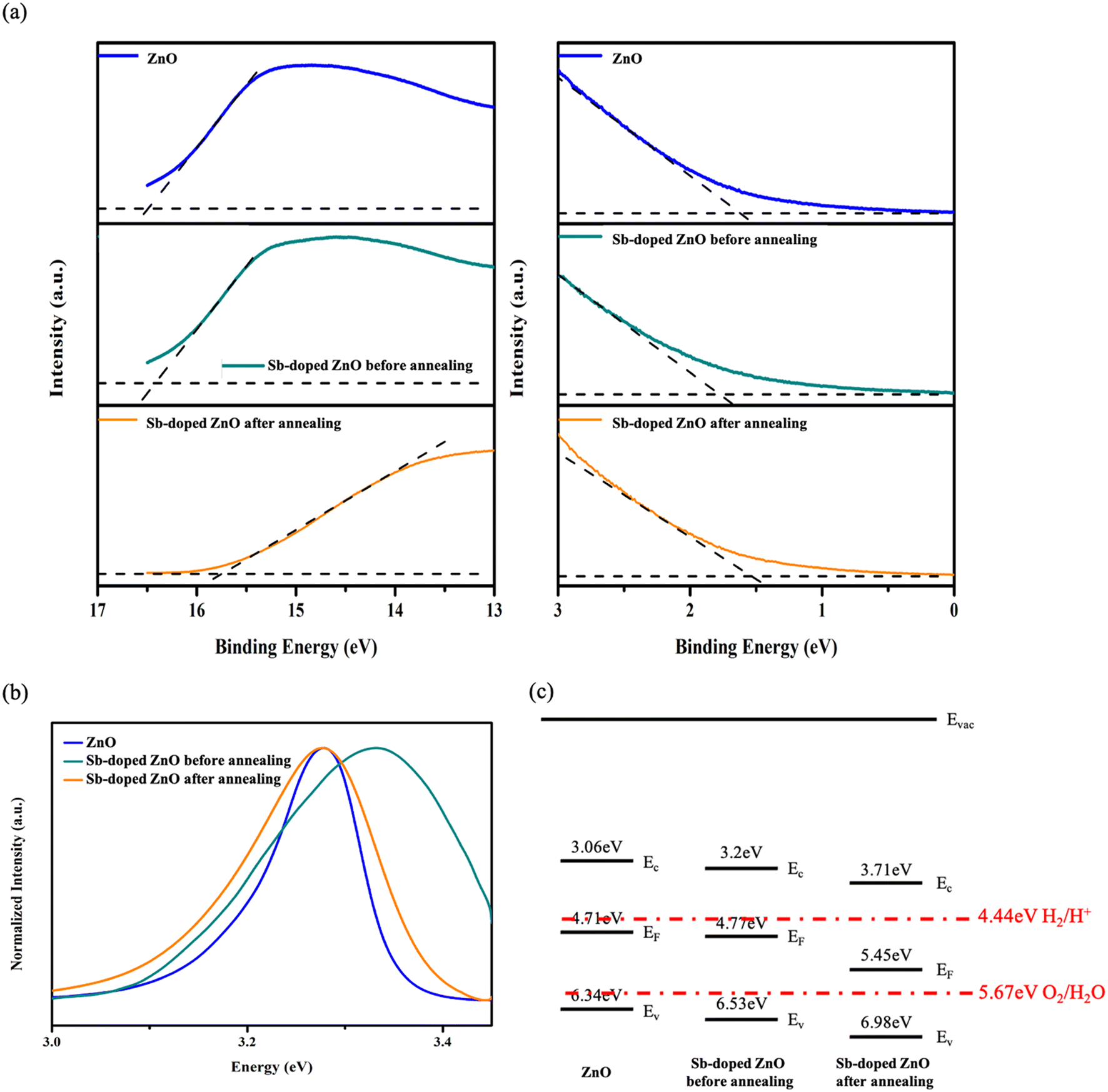 | ||
| Fig. 3 (a) UPS, (b) PL spectra and (c) derived energy band structure of ZnO, Sb-doped ZnO before annealing, and Sb-doped ZnO after annealing. | ||
Fig. S4† illustrates the dependence of piezoelectric output amplitude from PFM on AC voltages of 2 V, 4 V, 6 V, 8 V, and 10 V for ZnO, Sb-doped ZnO after annealing, annealed Sb-doped ZnO/ZnO, and PPLN. The PPLN sample was employed as a standard reference (d33 ∼ 25.2 pm V−1)25 to derive the effective piezoelectric coefficient, d33, for the other samples by comparing the slopes in Fig. 4(a) for calibration. The effective d33 values for ZnO, Sb-doped ZnO after annealing, and annealed Sb-doped ZnO/ZnO were 5.5 pm V−1, 7.4 pm V−1, and 3.51 pm V−1, respectively as shown in Fig. 4(b). The higher d33 of Sb-doped ZnO after annealing than the undoped ZnO is attributed to the higher degree of asymmetry in atomic structure from the doping-induced complex defects. On the other hand, the annealed Sb-doped ZnO/ZnO p–n homojunction exhibits the minimum d33, attributed to the influence of the built-in electric field, where the built-in electric field counteracts the applied AC bias, resulting in a decrease in output amplitude, further confirming the formation of the p–n junction.
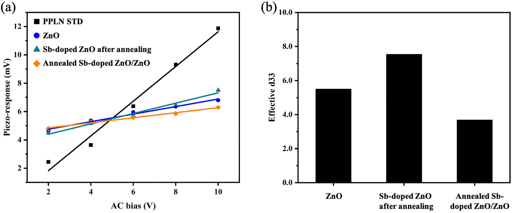 | ||
| Fig. 4 (a) Piezo-response analysis from PFM for ZnO, Sb-doped ZnO after annealing, annealed Sb-doped ZnO/ZnO, and PPLN as a reference. (b) Effective d33 of ZnO, Sb-doped ZnO after annealing, and annealed Sb-doped ZnO/ZnO. | ||
Examining the transient photocurrent response as a function of time as shown in Fig. 5(a), it can be observed that Sb-doped ZnO after annealing exhibits a 9.5% increase in current compared to ZnO, while annealed Sb-doped ZnO/ZnO shows the highest enhancement with 28.7% increase. This can be attributed to the formation of the built-in electric field in the depletion region of the p–n homojunction, thereby enhancing the separation of photo-generated carriers, as evidenced by the increase in flat band voltage in the Mott–Schottky analysis. However, as for the ZnO/annealed Sb-doped ZnO, its transient photocurrent response was the lowest among all the samples, as shown in Fig. S5(a).† According to the mechanism illustrated in Fig. S5(b),† the direction of the built-in electric field is unfavorable for carrier transport, which hinders electron flow to the external circuit and hole transport to the interface between the electrolyte and the material. This results in a significantly lower current compared to ZnO samples. The charge transfer process of the system was investigated through Electrochemical Impedance Spectroscopy (EIS) under illumination. Nyquist plots in Fig. 5(b) were fitted to the equivalent Randle circuit and were employed to evaluate the charge transfer resistance at the interface (Rct) between the photoelectrode and electrolyte. Rct can be evaluated from the diameter of the semicircle in the Nyquist plot, which is 22.6 kΩ, 10.9 kΩ, and 2.9 kΩ, respectively for undoped ZnO, Sb-doped ZnO after annealing and annealed Sb-doped ZnO/ZnO, and annealed Sb-doped ZnO/ZnO exhibits the smallest semicircle diameter and the lowest Rct to reach the electrolyte. The Bode phase plot and the calculated carrier transfer time constant (τct) are shown in Fig. S6.† By identifying the frequency (f) at the phase maximum, we calculated the τct,7 which is 4.3 ms, 10.0 ms, and 7.5 ms, respectively for undoped ZnO, Sb-doped ZnO after annealing and annealed Sb-doped ZnO/ZnO as shown in Fig. S6(b).† A longer charge transfer time constant indicates a lower probability of carrier recombination, which is more favorable for the PEC water-splitting reaction. Among all the samples, Sb-doped ZnO after annealing exhibited the longest charge transfer time constant. In addition, Sb-doped ZnO after annealing exhibits the highest conductivity among all the samples due to the formation of complex defects, while annealed Sb-doped ZnO/ZnO exhibits the lowest conductivity as shown in Fig. S7,† which indicates that carriers can more easily transport within Sb-doped ZnO after annealing. It can be concluded that Sb-doped ZnO after annealing demonstrates the highest charge separation efficiency since it possesses higher conductivity and exhibits higher carrier transfer time constant. Meanwhile EIS Nyquist plot analysis indicates that annealed Sb-doped ZnO/ZnO has the lowest interface resistance, thereby exhibiting the highest charge injection efficiency. Based on these results, the enhancement of the photocurrent of annealed Sb-doped ZnO/ZnO is not solely due to the electric field generated in the depletion region formed at the electrode–electrolyte interface, the built-in electric field at the homojunction interface, but also the carrier transfer enhancement with the material. Consequently, these mechanisms effectively reduce the rate of carrier recombination.
 | ||
| Fig. 5 (a) Transient photocurrent response as a function of time. (b) EIS Nyquist plot analysis. Linear sweep voltammetry measurement under applied tensile strain and compressive strain (from −0.15% to 0.15%) of (c) ZnO, (d) Sb-doped ZnO after annealing, and (e) annealed Sb-doped ZnO/ZnO homojunction. | ||
To further study the synergistic effects of piezoelectricity with doping and the formation of p–n homojunctions, linear sweep voltammetry (LSV) measurements of the PEC cells of all the samples were taken under mechanical strain of 0%, ±0.05%, ±0.1%, and ±0.15% as shown in Fig. 5(c)–(e). The schematic of the force applicator is depicted in Fig. S8,† where the position and rotation of the screw were utilized to regulate the degree of tensile or compressive strain (ε) using eqn (1):26
 | (1) |
Fig. 6 demonstrates the PEC mechanism of ZnO, Sb-doped ZnO after annealing, and annealed Sb-doped ZnO/ZnO. When subjected to downward bending, the substrate fixed on top experiences tensile stress causing compressive stress to the sample in the normal direction, leading to the generation of positive piezopotential at the bottom of the NRs and negative piezopotential at the top as shown in Fig. 6(a). In this case, several advantages can be expected. Firstly, the piezoelectric field aligns with the applied bias polarization in the PEC cell, thereby advancing the impact of the PEC cell bias. Secondly, the positive piezoelectric potential at the bottom facilitates the electron flow from the NRs to the external circuit by either lowering the energy barrier in ZnO or inducing downward band bending in Sb-doped ZnO after annealing and annealed Sb-doped ZnO/ZnO, promoting redox reactions. The negative piezoelectric potential at the top effectively enhances the flow of holes and hence the photocurrent toward the interface with electrolyte by simultaneously increasing the built-in electric field and the depletion region for ZnO and annealed Sb-doped ZnO/ZnO, suppressing the recombination rate of photo-generated carriers, while lowering the energy barrier for Sb-doped ZnO after annealing. Additionally, whether it be ZnO or Sb-doped ZnO after annealing acting as the photoelectrode, the upward shift in the valence band energy level caused by negative piezopotential becomes closer to the oxygen evolution reaction (OER) level for all the samples, which is advantageous for reducing the interface resistance through the piezocatalyst effect. Therefore, as a photoanode, holes are transferred to the interface between the material and the electrolyte, where they participate in the OER, as evidenced by the positive current observed in the linear sweep voltammetry measurement as shown in Fig. 5(c)–(e). Consequently, we can also infer that holes are transported to the solid–electrolyte interface for the reaction, while electrons flow through the external circuit to the counter electrode. Moreover, in the case of the annealed Sb-doped ZnO/ZnO, the built-in potential still dominates at the p–n homojunction, which is beneficial for the separation of photo-generated charge carriers, therefore resulting in the maximum response to changes in strain. Conversely, when subjected to upward bending, the NR photoelectrodes experience tensile stress from the normal direction, generating negative piezopotential at the bottom and positive piezopotential at the top, leading to a decrease in photocurrent. This effect occurs for several reasons. First, the piezoelectric polarization opposes the external bias. Furthermore, in ZnO, the negative piezoelectric field increases the energy barrier for electrons, hindering their transmission to the external circuit, while the positive piezoelectric potential reduces the depletion region of holes, impeding carrier separation efficiency. In the case of Sb-doped ZnO after annealing, both positive and negative piezopotentials at both ends increase the energy barrier for electrons and holes, hindering the transfer of carriers. Moreover, this positive piezopotential at the top causes the valence band of the photoelectrode to bend more downward, moving away from the OER level, increasing the interface impedance. In the case of annealed Sb-doped ZnO/ZnO, the combination of the disadvantages of both ZnO and Sb-doped ZnO after annealing leads to a more significant decrease in photocurrent under compressive strain. However, given the existence of three interfaces involving the bottom electrode, electrolyte, and annealed Sb-doped ZnO/ZnO homojunction, it is necessary to conduct a thorough analysis of the mutual interactions among these interfaces and their respective contributions to the current output.
 | ||
| Fig. 6 (a) Schematic of the sample under applied strain. Schematic energy band diagrams of (b) ZnO, (c) Sb-doped ZnO after annealing, and (d) annealed Sb-doped ZnO/ZnO under illumination and applied strain. | ||
Conclusion
In this research, we introduce a cost-effective and straightforward approach involving a two-step hydrothermal synthesis for the growth of a ZnO homojunction with precisely controlled Sb dopant distribution. This unique structural design efficiently diminishes interface transport impedance, contributing to the effective suppression of the recombination rate among photo-generated carriers. Additionally, the synergistic piezo-phototronic effect and piezocatalyst effect allow for the modulation of the Schottky barrier height and depletion region width, significantly improving the PEC efficiency. This study provides a simplified and economical method for synthesizing p–n homojunctions and contributes to the advancement of PEC water splitting systems thereby enhancing their output efficiency.Data availability
The data supporting this article have been included as part of the ESI.†Conflicts of interest
The authors declare no conflict of interest.Acknowledgements
The research was supported by National Science and Technology Council of Taiwan (Grant No. 113-2622-E-006-020, 113-2221-E-006-090-MY3, 113-2221-E-006-092-MY3, 113-2923-E-006-007-MY3), and Taiwan Space Agency of Taiwan (Grant No. TASA-S-1130061). The authors would like to thank Ms. Hui-Jung Shih with the Core Facility Center of National Cheng Kung University for supporting the use of HR-SEM (Hitachi SU8000) and EDS (BRUKER XFlash 5060F), and also gratefully acknowledge of XPS (PHI VersaProbe 4) belonging to the Core Facility Center of National Cheng Kung University in Taiwan.References
- F. Dawood, M. Anda and G. M. Shafiullah, Int. J. Hydrogen Energy, 2020, 45, 3847–3869 CrossRef CAS.
- J. D. Holladay, J. Hu, D. L. King and Y. Wang, Catal. Today, 2009, 139, 244–260 CrossRef CAS.
- M. G. Sürer and H. T. Arat, Eur. Mech. Sci., 2018, 2, 20–30 Search PubMed.
- V. Romano, G. D'Angelo, S. Perathoner and G. Centi, Energy Environ. Sci., 2021, 14, 5760–5787 RSC.
- T. Hisatomi, J. Kubota and K. Domen, Chem. Soc. Rev., 2014, 43, 7520–7535 RSC.
- C. H. Cheng, W. Y. Zhang, X. M. Chen, S. Q. Peng and Y. X. Li, Energy Sci. Eng., 2022, 10, 1526–1543 CrossRef CAS.
- S. Ju, H. J. Seok, J. Jun, D. Huh, S. Son, K. Kim, W. Kim, S. Baek, H. K. Kim and H. Lee, Appl. Catal., B, 2020, 263, 118362 CrossRef CAS.
- S. Q. Zhang, X. Liu, C. B. Liu, S. L. Luo, L. L. Wang, T. Cai, Y. X. Zeng, J. L. Yuan, W. Y. Dong, Y. Pei and Y. T. Liu, ACS Nano, 2018, 12, 751–758 CrossRef CAS PubMed.
- S. Jin, X. X. Ma, J. Pan, C. Y. Zhu, S. E. Saji, J. G. Hu, X. Y. Xu, L. T. Sun and Z. Y. Yin, Appl. Catal., B, 2021, 281, 119477 CrossRef CAS.
- H. J. Lv, H. F. Yin, T. J. Wang, W. G. Lin, C. Y. Yuan, Q. Fei, Y. J. Zhang, D. D. Xiao, X. Y. Wang, Y. Z. Zhang, P. Zhang and Q. K. Xue, Mater. Today Phys., 2023, 37, 101212 CrossRef CAS.
- Y. J. Ren, D. Q. Zeng and W. J. Ong, Chin. J. Catal., 2019, 40, 289–319 CrossRef CAS.
- D. L. Xiang, Z. R. Liu, M. Q. Wu, H. H. Liu, X. D. Zhang, Z. Wang, Z. L. Wang and L. L. Li, Small, 2020, 16, 1907603 CrossRef CAS.
- S. G. Shim, J. Tan, H. Lee, J. Park, J. Yun, Y. S. Park, K. Kim, J. Lee and J. Moon, Chem. Eng. J., 2022, 430, 133061 CrossRef CAS.
- D. Chen, Z. F. Liu, Z. G. Guo, W. G. Yan and M. N. Ruan, Chem. Eng. J., 2020, 381, 122655 CrossRef CAS.
- V. Soni, C. L. Xia, C. K. Cheng, V. Nguyen, D. L. Nguyen, A. Bajpai, S. Y. Kim, Q. Van Le, A. A. P. Khan, P. Singh and P. Raizada, Appl. Mater. Today, 2021, 24, 101074 CrossRef.
- Z. L. Wang, Nano Today, 2010, 5, 540–552 CrossRef CAS.
- L. P. Zhu and Z. L. Wang, J. Phys. D: Appl. Phys., 2019, 52, 343001 CrossRef CAS.
- N. Meng, W. Liu, R. Y. Jiang, Y. Zhang, S. Dunn, J. Y. Wu and H. X. Yan, Prog. Mater. Sci., 2023, 138, 101161 CrossRef CAS.
- L. Pan, S. C. Sun, Y. Chen, P. H. Wang, J. Y. Wang, X. W. Zhang, J. J. Zou and Z. L. Wang, Adv. Energy Mater., 2020, 10, 2000214 CrossRef CAS.
- X. Han, M. X. Chen, C. F. Pan and Z. L. Wang, J. Mater. Chem. C, 2016, 4, 11341–11354 RSC.
- S. Limpijumnong, S. B. Zhang, S. H. Wei and C. H. Park, Phys. Rev. Lett., 2004, 92, 155504 CrossRef PubMed.
- T. Yang, B. Yao, T. T. Zhao, G. Z. Xing, H. Wang, H. L. Pan, R. Deng, Y. R. Sui, L. L. Gao, H. Z. Wang, T. Wu and D. Z. Shen, J. Alloys Compd., 2011, 509, 5426–5430 CrossRef CAS.
- C. Cao, X. X. Xie, Y. M. Zeng, S. H. Shi, G. Z. Wang, L. Yang, C. Z. Wang and S. W. Lin, Nano Energy, 2019, 61, 550–558 CrossRef CAS.
- S. Pansri, R. Supruangnet, H. Nakajima, S. Rattanasuporn and S. Noothongkaew, J. Mater. Sci., 2020, 55, 4332–4344 CrossRef CAS.
- Z. Z. Hao, L. Zhang, A. Gao, W. B. Mao, X. D. Lyu, X. M. Gao, F. Bo, F. Gao, G. Q. Zhang and J. J. Xu, Sci. China: Phys., Mech. Astron., 2018, 61, 114211 Search PubMed.
- M. Wajahat, S. Lee, J. H. Kim, W. S. Chang, J. Pyo, S. H. Cho and S. K. Seol, ACS Appl. Mater. Interfaces, 2018, 10, 19999–20005 CrossRef CAS.
Footnote |
| † Electronic supplementary information (ESI) available. See DOI: https://doi.org/10.1039/d4cy00917g |
| This journal is © The Royal Society of Chemistry 2025 |