
 Open Access Article
 This Open Access Article is licensed under a Creative Commons Attribution-Non Commercial 3.0 Unported Licence
Layered tin halide perovskites in photovoltaics
Mengqiong
Zhu
a,
Bhumika
Chaudhary
bc,
Anamika
Mishra
b,
Michael
Saliba
 c and
Jovana V.
Milić
*ab
c and
Jovana V.
Milić
*ab
aAdolphe Merkle Institute, University of Fribourg, Switzerland. E-mail: jovana.milic@unifr.ch
bDepartment of Chemistry, University of Turku, Turku, Finland. E-mail: jovana.milic@utu.fi
cTechnical University of Darmstadt, Darmstadt, Germany. E-mail: michael.saliba@ipv.uni-stuttgart.de
First published on 18th November 2025
Abstract
Tin-based halide perovskites are emerging as promising alternatives to traditional lead-based perovskites due to their lower bandgaps, decreased toxicity, and comparable chemical properties. These materials offer unique structural and functional benefits for optoelectronic applications and photovoltaics, particularly in their low-dimensional or layered (2D) forms. Recent advancements have improved the solar-to-electric power conversion efficiency of tin-based halide perovskites by relying on organic spacers to control crystallisation and stabilise the materials. The versatility of molecular compositions and structural tuning of layered tin halide perovskites makes them appealing for next-generation photovoltaic technologies. This review highlights the structural characteristics, synthetic methods, and properties of layered tin halide perovskites, providing a comprehensive overview and discussing future prospects for environmentally friendly perovskite photovoltaics.
 Mengqiong Zhu | Mengqiong Zhu obtained her BS (2020) from Huazhong University of Science and Technology and her MS (2023) from Sun Yat-sen University, China. She began her PhD at the Adolphe Merkle Institute, University of Fribourg, Switzerland, as a CSC Fellow, focusing on layered tin perovskite photovoltaics, and later moved to the Zernike Institute for Advanced Materials, University of Groningen, the Netherlands, where she continues to work on layered tin and tin–lead perovskite optoelectronics. |
 Bhumika Chaudhary | Bhumika Chaudhary received her PhD from Nanyang Technological University, Singapore, where she focused on engineering multi-dimensional perovskites for enhanced thermal stability in solar cells. She has been a postdoctoral researcher at the Institute for Photovoltaics, University of Stuttgart, Germany, working on improving the performance and stability of perovskite photovoltaic devices through interfacial passivation and additive engineering. |
 Anamika Mishra | Anamika Mishra has been a postdoctoral researcher at the Department of Chemistry, University of Turku, Finland, since September 2024. She obtained her PhD in 2022 from the CSIR-National Physical Laboratory in New Delhi, India. She worked as Fulbright Doctoral Researcher at Rice University and as a postdoctoral researcher at the University of South Florida in USA. Her research focuses on functional organic systems for perovskite framework materials and their application in smart energy conversion technologies, such as photovoltaics and biosensing. |
 Michael Saliba | Michael Saliba is the Director of the Institute for Photovoltaics (ipv) at the University of Stuttgart with a dual appointment as the Helmholtz Young Investigator at the Forschungszentrum Jülich, Germany. He obtained his PhD at Oxford University in the UK. His research focuses on a deeper fundamental understanding and improvement of optoelectronic properties of emerging photovoltaic materials with an emphasis on perovskites for a sustainable energy future. Among others, he received the Heinz-Maier-Leibnitz Award of the German Research Foundation and was named as one of the worldwide 35 innovators under 35 by the MIT Technology Review. |
 Jovana V. Milić | Jovana V. Milić has been an Associate Professor at the Department of Chemistry of the University of Turku in Finland since September 2024. She obtained her Dr. Sc. Degree in the Department of Chemistry and Applied Biosciences at ETH Zurich in Switzerland in 2017. She then worked as a Scientist in the Laboratory of Photonics and Interfaces at EPFL and as an Assistant Professor at the Adolphe Merkle Institute of the University of Fribourg in Switzerland. Her research is centered around bioinspired stimuli-responsive (supra)molecular materials for energy conversion, with a particular interest in photovoltaics and neuromorphic computing for smart and sustainable (nano)technologies. |
1. Introduction
The emergence of metal halide perovskites as one of the most promising photovoltaic materials has stimulated interest in lead-free and tin-based perovskites (Info Box 1).1–3 Traditional lead-based perovskites pose significant environmental hazards due to their toxicity, making tin, with its similar chemical characteristics, one of the most relevant substitutes.4 Additionally, the narrow bandgap of Pb–Sn mixed perovskites renders them promising candidates in multijunction applications.5 However, Sn-based perovskites face challenges, such as rapid crystallisation and the susceptibility of Sn(II) to oxidation, leading to high self-p-doping and excessive defects that significantly impact device efficiency and operational stability.6 Recent advancements employing low-dimensional and layered (2D) perovskites have effectively enhanced the efficiency of Sn-based perovskites from 6.4% to 17.1%.7–9 This involves the use of organic spacer layers that template low-dimensional or 2D perovskite architectures, which decelerate the crystallisation rate while inducing preferred orientation and protecting the 3D perovskites from water and oxygen, resulting in suppressed self-doping and ion migration.7,8,10Layered tin-based halide perovskites (LTHPs) have attracted considerable attention in recent years due to their unique structural and optoelectronic properties.7,8 These materials are characterised by layered (2D) architecture templated by organic cations, offering a versatile platform for various applications in the field of optoelectronics and photovoltaics in particular. LTHPs can be described by S2An−1SnnX3n+1 or S′An−1SnnX3n+1 formulae, where A are central A-cations, X halide anions, and S or S′ organic spacer cations (typically mono- or bifunctional ammonium cations, respectively), which often form Ruddlesden–Popper (RP) and Dion–Jacobson (DJ) phases. This allows for a wide range of material compositions and dimensional tuning.11–15 This diversity of materials not only offers versatile structures and related properties, such as conductivity and stability, but also opens up new avenues for multifunctionality.16,17 The ability to fine-tune the functional properties of LTHPs via molecular engineering makes them highly attractive for next-generation photovoltaics.
In this review, we discuss the emergence of tin-based layered perovskites with respect to their potential and recent advancements. We explore the synthesis methods, structural characteristics, and photovoltaic properties of these materials, highlighting key breakthroughs in the field. This provides a comprehensive overview of the current state and future prospects of layered tin-based halide perovskite materials and devices, with the aim of providing a valuable resource for researchers and practitioners looking to develop environmentally friendly high-performance photovoltaics.
Info Box 1. A brief history and definition of LTHPsPerovskites were first discovered in 1839 in the Ural Mountains by Gustav Rose, a mineralogist at the University of Berlin.18 They were named after the Russian nobleman and mineralogist Lev Perovski, and are based on the AMX3 composition defining a corner-sharing {MX6} octahedral framework, including divalent metal (M) cations (mostly Pb2+ or Sn2+), X halide (I−, Br−, Cl−) anions, and central (A+) cations, which can be either organic (such as methylammonium (MA+), formamidinium (FA+), etc.) or inorganic (such as Cs+) species.16 Halide perovskites are soft mixed ionic-electronic conductors that exhibit excellent light absorption, as well as long lifetimes and diffusion lengths of photogenerated charge carriers, with exceptional defect tolerance, which results in remarkable performances in optoelectronic devices, such as solar cells, light-emitting diodes, and brain-inspired memories.16 The emergence of layered halide perovskites marks an important milestone in perovskite material research (Fig. 1). The first inorganic layered perovskite was the Ruddlesden–Popper phase perovskite.21 Layered tin hybrid perovskites (LTHPs) were formed by substituting the A-site anions with large molecular species by Mitzi and colleagues, who revealed the semiconductor properties of layered perovskites in 1990s.24 LTHPs are commonly based on SxAn−1SnnX3n+1 compositions including organic (typically ammonium) cations, which are either mono- (x = 2) or bifunctional (x = 1) spacers (S) between perovskite layers.16 Further interest in 3D and 2D perovskites stems from the demonstration of perovskite-based solar cells in 2009,22 when Miyasaka and co-workers first employed organic–inorganic hybrid perovskite materials, methylammonium lead iodide (CH3NH3PbI3) and methylammonium lead bromide (CH3NH3PbBr3), as new photosensitizers to fabricate the first functional perovskite solar cell. Since then, LHPs have emerged as attractive materials due to higher environmental and operational stabilities as compared to their 3D perovskite analogues.16 Currently, perovskite cells have achieved a single-junction efficiency of 27.0% and a silicon-perovskite tandem efficiency of 34.6%, showing broad market prospects.23 However, lead-based perovskites pose serious environmental issues, prompting the exploration of tin-based halide perovskites. The development of tin-based and their layered perovskites benefited from the outstanding performance of lead halide perovskites and the efforts to advance sustainability. In 2012, the first tin-based perovskite cell had an efficiency of only 0.6%,28 but through optimising the device structure, the efficiency increased to 6%.29,30 To overcome the rapid crystallisation and significant defects caused by tin oxidation in tin-based perovskites, LTHPs were introduced, attracting significant research interest. In 2017, Ning and colleagues further studied these materials, and by 2024, the efficiency reached a certified 15.7%.9 Future material design is expected to further advance the LTHPs. |
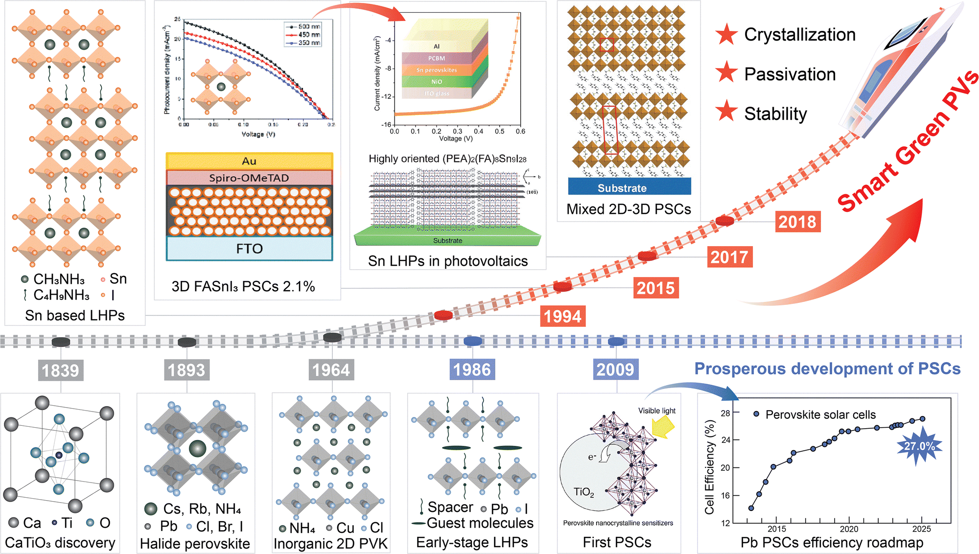 | ||
| Fig. 1 Development of layered tin halide perovskites. Schematic overview of historical developments in the emergence of tin-based perovskite solar cells based on ref. 18–27. Some of the panels are reproduced with permission from ref. 22 (Copyright 2009 American Chemical Society), ref. 24 (Copyright 1994 Springer Nature), ref. 25 (Copyright 2013 Royal Society of Chemistry), ref. 26 (Copyright 2017 American Chemical Society), and ref. 27 (Copyright 2017 John Wiley and Sons). | ||
2. Versatile layered tin perovskite structure
Layered tin halide perovskites (LTHPs) consist of hybrid halide perovskite layers that are templated by organic spacers, linking adjacent perovskite slabs while assembling via different types of noncovalent interactions, such as hydrogen bonding (HB), van der Waals (vdW), and π-based interactions, among others (Fig. 2).31 Designing organic spacers and related LHP structures, such as by tailoring their interactions, can enable desired properties for photovoltaics and other optoelectronic applications.13 The structural versatility of LTHPs is considered from the perspective of organic spacers (Fig. 2) and perovskite phases, defining their structure–property relations.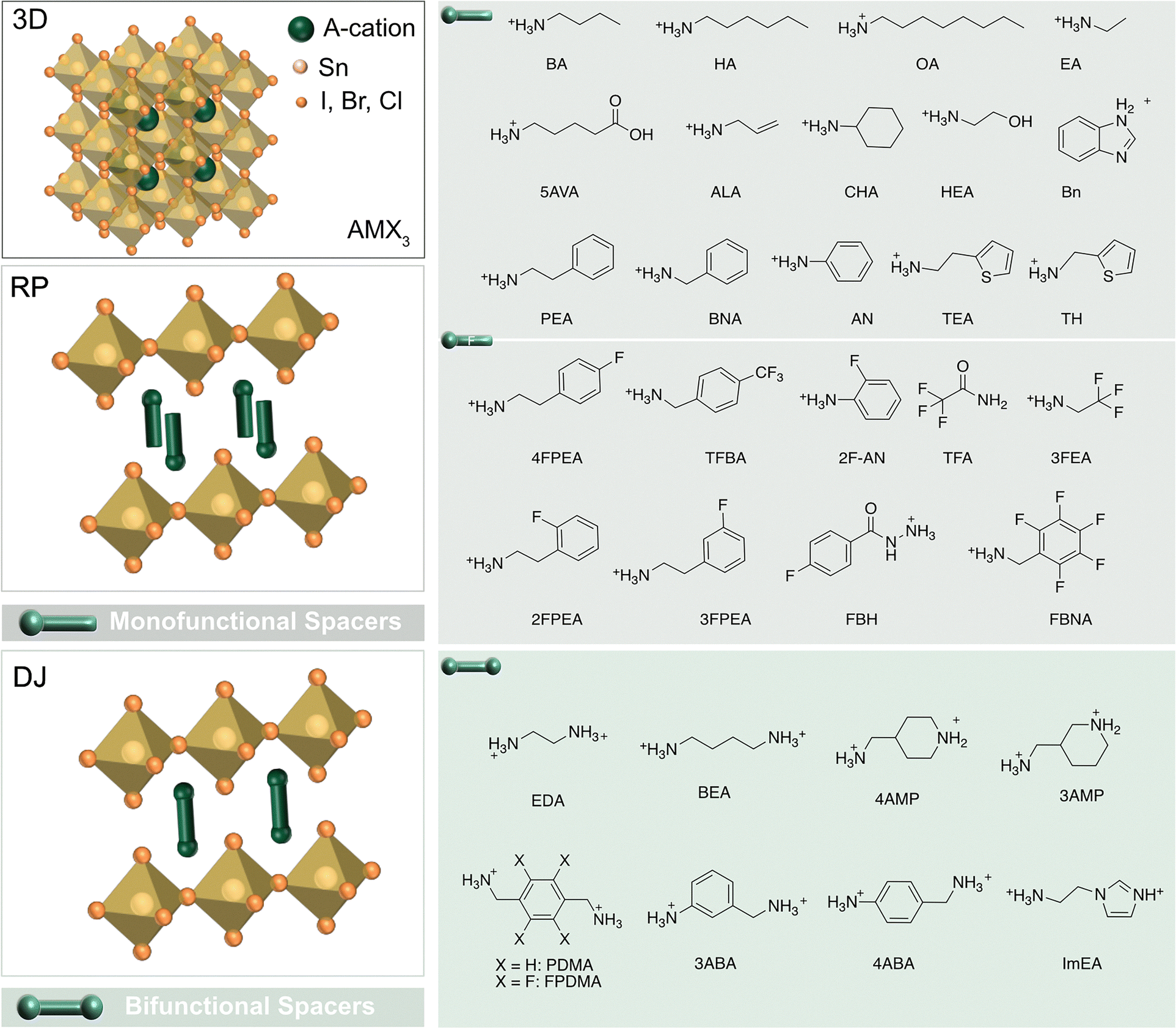 | ||
| Fig. 2 Layered tin halide perovskite structure. Three-dimensional (3D, top left) tin halide perovskite defined by ASnX3 composition with the corresponding components (X = I, Br, Cl). Two-dimensional (2D, bottom left) Sn halide perovskite phases, including Ruddlesden–Popper (RP) and Dion–Jacobson (DJ) phases (represented by n = 1 structural representatives) with the corresponding mono- (top right) and bifunctional (bottom right) spacers, including fluorinated (F) derivatives (middle). Further structural details are provided in Table 1. | ||
Organic spacers can template layered (2D) perovskites.11,15,19 They are typically described by the S2An−1MnX3n+1 or S′An−1MnX3n+1 formulae, where Pb is substituted by Sn at the M site, and n defines the number of inorganic layers held together. A (methylammonium (MA+), formamidinium (FA+), Cs+) are central A-cations, X halide anions (Cl−, Br−, I−), and S or S′ are typically mono- or bifunctional ammonium cations, respectively, which often form Ruddlesden–Popper (RP) or Dion–Jacobson (DJ) 2D halide perovskite phases (Fig. 2).13
RP and DJ phases are defined by the corresponding alignment of the adjacent perovskite slabs that feature half-a-unit-cell displacement for RP and no displacement for DJ phases (Fig. 2).32 Archetypical RP phases are based on the formula S2An−1MnX3n+1 and monofunctional spacer (S) bilayers templating perovskite layers displaced along both in-plane directions.33 Conversely, the DJ phases are often defined by the S′An−1MnX3n+1 formula with the aligned adjacent perovskite layers without any relative displacement.14 The commonly used bifunctional spacers in DJ phases facilitate stronger interactions between the layers, resulting in more compact and rigid structures.13,14 In the intermediary case, the less common alternating cation (AC) systems form that are based on two organic cations and feature a displacement by half a crystal unit cell along one of the in-plane directions.16 LTHPs can be further classified based on different n values, which are determined by the number of inorganic layers separated by organic spacer cations, approaching the characteristics of the 3D perovskite framework with the increasing number of layers (n).34 Following the development of Pb-based LHPs, a wide variety of organic spacer cations have also been explored for Sn-based derivatives, while the ongoing research targeting the unique properties of Sn perovskites continues to expand this family of materials.7,8
There are geometric constraints for organic molecules to be incorporated into the perovskite framework as spacer layers that translate into molecular design rules for LTHPs.13 The primary criteria for selecting spacer cations include their overall molecular geometry, i.e., size and shape. The size of A cations for 3D perovskite is limited by the Goldschmidt tolerance factor (defined by eqn (1))35 as follows
| t = (rA + rX)/[√2(rM + rX)] | (1) |
Linear or cyclic aliphatic cations with ammonium groups were amongst the first spacers explored in LHPs (Fig. 2 and Table 1). As early as 1994, Mitzi et al. reported a class of LTHPs based on archetypical n-butylammonium (BA) spacers, denoted as BA2MAn−1SnnI3n+1.24 These materials exhibited a transition from semiconductor to metallic behaviour as the value of n increased. In 2017, Kanatzidis et al. developed LTHPs for photovoltaics with the same composition (n = 1–4), demonstrating high resistivity and excellent stability against humidity.44 In recent years, this scope has expanded to other derivatives, including cyclic hydrocarbons. By adjusting the number of amino groups and the carbon chain length, this family of aliphatic spacers can be expanded. For instance, in 2021, Diau et al. studied cyclic cyclohexylammonium (CHA) in Sn perovskite solar cells.45 The effects of alkyl chain length on crystal growth and oxidation process of LTHPs were studied by Liu et al. based on BA, n-octylammonium (OA), and n-dodecylammonium (DA) cations, showing shorter alkylamines exhibited better orientation.46 These spacers can be further tailored by incorporating other functional groups, such as the carboxylic (–COOH) and hydroxyl (–OH) ones. For instance, Yuan et al. studied LTHPs using 5-ammoniumvaleric acid (5AVA), which features an additional carboxylic group (–COOH) on the carbon chain, enabling complementary hydrogen bonding interactions in the organic spacer layer,47 which can significantly influence their crystallisation and contribute to material quality.
| No. | Spacer | Interaction | Composition | Phase | Bandgap (eV) | Device structure | PCE | Stability | Year | Ref. | |
|---|---|---|---|---|---|---|---|---|---|---|---|
| 3ABA = 3-aminobenzylamine; 4ABA = 4-aminobenzylamine; 5AVA = 5-ammoniumvaleric acid; ALA = allylammonium; 4AMP = 4-(aminomethyl)piperidine; 3AMPY = 3-(aminomethyl)pyridinium; AN = anilinium; BA = n-butylammonium; BAAc = n-butylammonium acetate; BCP = 2,9-dimethyl-4,7-diphenyl-1,10-phenanthroline; BEA = 1,4-butane-diammonium; Bn = benzimidazole; BNA = benzylammonium; C60-ETPA = C60 with external triphenylamine group; CHA = cyclohexylammonium; c-TiO2 = compact titanium dioxide; DA = dodecylammonium; EA = ethylammonium; EDA = ethylenediammonium; 2F-AN = 2-fluoro-anilinium; FA = formamidinium; FBH = 4-fluorobenzohydrazide; FBNA = 2-(perfluorophenyl)methylammonium; 3FEA = trifluoroethylamine; 2FPEA = 2-fluoro-phenethylammonium; 3FPEA = 3-fluoro-phenethylammonium; 4FPEA = 4-fluoro-phenethylammonium; FTO = fluorine-doped tin oxide; GA = guanidinium; HA = hexylammonium; HB = hydrogen bonding; HEA = hydroxyethylammonium; ICBA = indene-C60 bis-adduct; ImEA = 1-(2-ammonioethyl)-1H-imidazol-3-ium; ITO = indium-doped tin oxide; MA = methylammonium; m-TiO2 = mesoporous titanium dioxide; OA = octylamine; P3HT = poly(3-hexylthiophene-2,5-diyl); PDMA = 1,4-phenyldimethylammonium; PEA = 2-phenylethylammonium; PEDOT = poly(3,4-ethylenedioxythiophene); PEDOT:PSS = poly(3,4-ethylenedioxythiophene):poly(styrenesulfonate); PCBM = [6,6]-phenyl-C61-butyric acid methyl ester; PTAA = poly[bis(4-phenyl)(2,4,6-trimethylphenyl)amine; TEA = 2-thiophene ethylammonium; TFA = trifluoroacetamide; TFBA = 4-(trifluoromethyl)benzylammonium; TH = 2-thiophene methylammonium; vdW = van der Waals; XB = halogen bonding; π = π-based interactions. | |||||||||||
| 1 | BAI | HB, vdW | (BA)2(MA)2Sn3I10 | RP | n = 3 | 1.50 | FTO/TiO2/PVK/PTAA/Au | 2.53% | 30 min in air 1 month (encapsulated), 10% decay | 2017 | 44 |
| 2 | BAI 15% in FASnI3 | RP | Quasi-2D | 1.40 | ITO/PEDOT:PSS/PVK/C60/BCP/Ag | 8.9% | 1600 h, no decay | 2018 | 69 | ||
| 3 | BA2MA3Sn4I13 | RP | Quasi 2D | — | ITO/SnO2/PVK/PCBM/LiF/Al | 4.03% | 94 d in N2, no decay | 2019 | 70 | ||
| 4 | BA2FA3Sn4I13 | RP | Quasi-2D | 1.43 | FTO/TiO2/PVK/PTAA/Au | 4.04% | 14 d in N2, 20% decay | 2020 | 46 | ||
| 5 | Surface treatment FA0.8GA0.2SnI3 | RP | 2D–3D | — | ITO/PEDOT:PSS/PVK/C60/BCP/Ag | 9.1% | Over 150 h in air | 2021 | 45 | ||
| 6 | 5AVAI | HB, vdW | AVA2FA4Sn5I16 | RP | Quasi-2D | — | ITO/PEDOT:PSS/PVK/PCBM/BCP/Ag | 8.71% | 12 h in air | 2019 | 47 |
| 7 | OAI | HB, vdW | OA2FA3Sn4I13 | RP | Quasi-2D | 1.43 | FTO/TiO2/PVK/PTAA/Au | 2.99% | 14 d in N2, 20% decay | 2020 | 46 |
| 8 | DAI | HB, vdW | DA2FA3Sn4I13 | RP | Quasi-2D | 1.54 | FTO/TiO2/PVK/PTAA/Au | 2.41% | 14 d in N2, 20% decay | 2020 | 46 |
| 9 | BEAI2 | HB | (BEA)FA2Sn3I10 | DJ | n = 3 | 1.34 | ITO/PEDOT:PSS/PVK/PCBM/Ag | 6.43% | 200 h in air, 10% decay | 2020 | 61 |
| 10 | EDAI2 | HB | Surface treatment GeI2 doped (FA1−xEAx)0.98EDA0.01SnI3 | DJ | 2D–3D | 1.42 | FTO/PEDOT:PSS/PVK/P3HT/Ag/Au | 13% | — | 2020 | 38 |
| 11 | HAI | HB, vdW | Surface treatment FA0.8GA0.2SnI3 | RP | 2D–3D | 1.50 | ITO/PEDOT:PSS/PVK/C60/BCP/Ag | 8.4% | — | 2021 | 45 |
| 12 | ALAI | HB, vdW | (ALA)2(FA)24Sn25I76 | RP | Quasi-2D | 1.38 | ITO/PEDOT:PSS/PVK/C60/BCP/Ag | 9.32% | 2400 h in N2, less than 10% decay | 2020 | 71 |
| 13 | ALAI | HB, vdW | Surface treatment FA0.8GA0.2SnI3 | RP | 2D–3D | 1.50 | ITO/PEDOT:PSS/PVK/C60/BCP/Ag | 9.3% | — | 2021 | 45 |
| 14 | CHAI | HB, vdW | Surface treatment FA0.8GA0.2SnI3 | RP | 2D–3D | 1.50 | ITO/PEDOT:PSS/PVK/C60/BCP/Ag | 7.8% | — | 2021 | 45 |
| 15 | PEAI | HB, π, vdW | (PEA)2FA8Sn9I28 | RP | Quasi-2D | — | ITO/NiOx/PVK/PCBM/Al | 5.94% | 100 h in N2, retain 96% | 2017 | 26 |
| 16 | (PEA,FA)SnI3 | RP | 2D–3D | 1.38 | ITO/PEDOT:PSS/PVK/C60/BCP/Ag | 6.98% | 400 s steady output power | 2018 | 72 | ||
| 17 | PEA2FA24Sn25I76 | RP | Quasi-2D | — | ITO/PEDOT:PSS/PVK/C60/BCP/Al | 9.00% | 2 h under AM1.5G in N2, no degradation | 2018 | 27 | ||
| 18 | PEA0.15FA0.85SnI3 | RP | Quasi-2D | 1.39 | ITO/NiOx/PVK/PCBM/BCP/Al | 9.41% | 600 h in N2, 10% decay | 2018 | 73 | ||
| 19 | (BA0.5PEA0.5)2FA3Sn4I13 | RP | Quasi-2D | — | ITO/PEDOT:PSS/PVK/C60/LiF/Ag | 8.82% | 24 d in N2, 40% decay | 2019 | 74 | ||
| 20 | PEA0.15FA0.85SnI3 | RP | Quasi-2D | 1.39 | ITO/PEDOT/PVK/ICBA/BCP/Ag | 12.4% | 3800 h in N2, retain 90% | 2020 | 75 | ||
| 21 | PEA2SnI4 + MASnI3 | RP | 2D–3D | — | FTO/PEDOT:PSS/PVK/C60/Au | 9.8% | 24 h, drop to 12% of initial PCE | 2020 | 76 | ||
| 22 | Surface treatment FA0.8GA0.2SnI3 | RP | 2D–3D | 1.50 | ITO/PEDOT:PSS/PVK/C60/BCP/Ag | 9.6% | 20 h in air, 20% decay | 2021 | 45 | ||
| 23 | PEA0.1(FA0.75MA0.25)0.9SnI3 | RP | Quasi-2D | 1.33 | ITO/PEDOT:PSS/PVK/ICBA/BCP/Ag | 10.46% | 700 h in N2, retain over 75% | 2021 | 77 | ||
| 24 | (BAAcO0.3PEA0.7)2FA3Sn4I13 | RP | Quasi-2D | — | ITO/PEDOT:PSS/PVK/ICBA/LiF/Ag | 10.36% | 600 h in N2, retain over 90% | 2021 | 78 | ||
| 25 | PEABr | HB, π, vdW | Bottom treatment FASnI3 | RP | 2D–3D | — | ITO/PEDOT:PSS/PVK/C60/BCP/Cu | 7.05% | 200 s steady output power | 2018 | 79 |
| 26 | Surface treatment FASnI3 | RP | 2D–3D | 1.40 | ITO/PEDOT:PSS/PVK/PCBM/BCP/Al | 7.86% | 350 h under AM1.5G, retain 80% | 2019 | 80 | ||
| 27 | EA-modified FASnI3 BAAc additive | RP | Quasi-2D | — | FTO/PEDOT:PSS/PVK/C60/BCP/Ag | 10.4% | >1000 h in N2, retain 96% T80 = 400 h | 2021 | 81 | ||
| 28 | 4AMP | HB, π | (4AMP)SnI4 | DJ | n = 1 | — | FTO/TiO2/ZrO2/PVK/C | 2.15% | — | 2018 | 51 |
| 29 | (4AMP)FA3Sn4I13 | DJ | Quasi-2D | 1.47 | FTO/TiO2/ZrO2/PVK/C | 4.22% | 100 h in N2 at 45 °C under AM1.5G 10% decay | 2018 | 51 | ||
| 30 | Bn | π, vdW | Bn2SnI4 | RP | n = 1 | 1.81 | FTO/c-TiO2/m-TiO2/PVK/Au | 2.35% | 5 min MPPT | 2019 | 55 |
| 31 | AN | HB, π, vdW | Surface treatment FA0.8GA0.2SnI3 | RP | 2D–3D | 1.50 | ITO/PEDOT:PSS/PVK/C60/BCP/Ag | 10.4% | Over 150 h in air | 2021 | 45 |
| 32 | ImEA | HB, π | (ImEA)SnI4 | DJ | n = 1 | 2.02 | ITO/PEDOT:PSS/PVK/PCBM/BCP/Al | 2.26% | — | 2021 | 63 |
| 33 | TEAI | HB, π, vdW | 0–40%, MASnI3 | RP | Quasi-2D | ∼1.27 | ITO/PEDOT:PSS/PVK/PCBM/BCP/Ag | 6.80% | 200 s steady output power | 2022 | 53 |
| 34 | PEASCN | HB, π, vdW | 15%, FA0.75MA0.25SnI2.75 Br0.25 | RP | Quasi-2D | — | ITO/NiOx/PVK/C60-ETPA/BCP/Ag | 12.88% | 2000 h in N2, retain over 80% | 2023 | 82 |
| 35 | THI | HB, π, vdW | TH2FA3Sn4I13 | RP | Quasi-2D | 1.33 | ITO/PEDOT:PSS/PVK/PCBM/BCP/Ag | 9.03% | 24 h in air, retain over 90% | 2023 | 54 |
| 36 | BNAI | HB, π, vdW | BNA2FA3Sn4I13 | RP | Quasi-2D | 1.33 | ITO/PEDOT:PSS/PVK/PCBM/BCP/Ag | 4.04% | 24 h in air, decrease by 50% | 2023 | 54 |
| 37 | PDMABr | HB, π | (FA,EA,PEA)SnI3 (antisolvent) | DJ | 2D–3D | — | FTO/PEDOT:PSS/PVK/C60/BCP/Ag | 11.44% | 200 h in 10% RH N2, retain over 90% | 2024 | 10 |
| 38 | 3ABAI2 | HB, π | (3ABA)FA4Sn5I16 | DJ | n = 5 | 1.44 | ITO/PEDOT:PSS/PVK/C60/BCP/Cu | 6.81% | 840 h in N2, retain 95% | 2024 | 56 |
| 39 | 4ABAI2 | HB, π | (4ABA)FA4Sn5I16 | DJ | n = 5 | 1.47 | ITO/PEDOT:PSS/PVK/C60/BCP/Cu | 5.25% | 840 h in N2, retain 92% | 2024 | 56 |
| 40 | 3AMPYI | HB, π | (3AMPY)SnI4 in PEA,FASnI3 | DJ | Quasi-2D | 1.38 | ITO/PEDOT:PSS/PVK/C60/BCP/Ag | 13.28% | 3000 h in N2, retain 96% | 2025 | 52 |
| 41 | TFBAI | HB, π, vdW | (TFBA2SnI4)x(FASnI3)1−x | RP | 2D–3D | 1.52 | ITO/PEDOT:PSS/PVK/C60/BCP/Ag | 11% | 100 h at 60 °C in RH 60% under AM 1.5G, less than 5% loss | 2020 | 83 |
| 42 | 4FPEABr | HB, π, vdW | FPEA0.1FA0.9 SnI2.9Br0.1 | RP | Quasi-2D | 1.43 | ITO/PEDOT:PSS/PVK/ICBA/BCP/Ag | 14.81% | 432 h in N2 (encapsulated), retain 80% | 2021 | 60 |
| 43 | 2FPEA | HB, π, vdW | Surface treatment FA0.8GA0.2SnI3 | RP | 2D–3D | 1.50 | ITO/PEDOT:PSS/PVK/C60/BCP/Ag | 8.3% | — | 2021 | 45 |
| 44 | 2F-AN | HB, π, vdW | Surface treatment FA0.8GA0.2SnI3 | RP | 2D–3D | 1.50 | ITO/PEDOT:PSS/PVK/C60/BCP/Ag | 8.9% | — | 2021 | 45 |
| 45 | 3FPEAI | HB, π, vdW | 8%, FASnI3 | — | Molecular passivation | 1.41 | ITO/PEDOT:PSS/PVK/C60/BCP/Ag | 9.40% | — | 2020 | 84 |
| 46 | 2FPEAI | HB, π, vdW | 8%, FASnI3 | — | Molecular passivation | 1.41 | ITO/PEDOT:PSS/PVK/C60/BCP/Ag | 10.17% | >1600 h in N2, 15% loss | 2020 | 84 |
| 47 | FBH | HB, π, vdW | Surface treating FASnI3 | — | Molecular passivation | — | ITO/PEDOT:PSS/PVK/C60/BCP/Ag | 9.47% | 600 h MPPT in N2, retain over 96% | 2020 | 85 |
| 48 | 3FEAI | HB, π, vdW | Surface treating FASnI3 | — | Molecular passivation | 1.41 | ITO/PEDOT:PSS/PVK/C60/BCP/Ag | 9.34% | 500 h in N2, retain 90% | 2021 | 86 |
| 49 | TFA | HB, vdW | Surface treating FASnI3 | — | Molecular passivation | 1.42 | ITO/PEDOT:PSS/PVK/C60/BCP/Ag | 11.74% | 1800 h in N2, less than 14% decay | 2023 | 87 |
| 50 | FBNA | HB, π, vdW | Surface treating FASnI3 | — | Molecular passivation | 1.4 | ITO/PEDOT/PVK/C60/BCP/Ag | 9.1% | 50 days in N2, retain 87.5% | 2025 | 59 |
| 51 | EAI | HB, vdW | EAxMA(0.98−x)SnI3 (x = 0–0.8) | — | Hollow | 1.44 | ITO/PEDOT:PSS/PVK/PCBM/BCP/Ag | 9.24% | 30 days in N2, retain 95% | 2020 | 62 |
| 52 | HEAI | HB, vdW | HEAxFA1−xSnI3 (x = 0–1) | — | Hollow | 1.53 | FTO/TiO2/Al2O3/PVK/carbon | 3.90% | 340 h in N2, reach max PCE | 2018 | 40 |
In addition, aromatic cations with phenyl or pyridine groups were widely studied in LHPs, featuring complementary π-based interactions.48 These result from electrostatic interactions and fluctuating polarisations determined by the quadrupole moments of the π systems, including π–π and π–ion interactions of aromatic spacers, templating the layered structure.49 One of the most widely used aromatic spacers in 2D Pb- and Sn-based perovskites is 2-phenylethylammonium (PEA). In 1999, Mitzi and co-workers studied 2D (PEA)2SnI4 thin films in transistors, achieving field-effect mobilities of 0.6 cm2 V−1 s−1.50 PEA spacer was first used in Sn-based perovskite photovoltaics by Ning et al. in 2017.26 They optimised the PEA ratio in the precursor solution, leading to the highly oriented growth of low-dimensional Sn-based perovskite films. Similarly, heterocyclic derivatives, including pyridine and thiophene, were also investigated, which involved 4-(aminomethyl)piperidine (4AMP),51 3-(aminomethyl)pyridinium) (3-AMPY),52 2-thiopheneethylammonium (TEA),53 and 2-thiophene methylammonium (TH) moieties.54 These spacers are found to form 2D phases and exhibit high orientation with a low Sn4+ content. Finally, Zimmermann et al. introduced benzimidazole (Bn) and benzodiimidazolium (Bdi) spacers.55 Other aromatic spacers that are derivatives of PEA (such as PEA-SCN) and benzylammonium (BNA)54 analogues, such as 3-aminobenzylamine (3ABA)56 and 4-aminobenzylamine (4ABA),56 or anilinium (AN),45 were also studied in Sn perovskite solar cells (Fig. 2 and Table 1), showing improved crystallisation and operational stability. The aromatic spacers also feature additional vdW forces and π interactions, which provide further stability enhancement and orientation control. Moreover, σ-hole interactions, such as halogen bonding (XB)48,57,58 and chalcogen bonding (ChB),58 are alternative interactions for LTHP with uniquely directional nature, which can influence the orientation.48 Functionalising linear and aromatic spacers with halogen atoms has been a common strategy to introduce XB.49,57 Moreover, (per)fluoroarenes are particularly attractive due to their hydrophobicity and dipole characteristics.49 Fluoroarenes applied to LTHPs include 4-fluoro-phenethylammonium (FPEA) and 2-(perfluorophenyl)methylammonium (FBNA).59 He et al. also demonstrated that a 2D Sn perovskite encapsulation layer based on FPEA can create a reducing atmosphere for the 3D FASnI3 grains.60 This unique microstructure effectively prevented the oxidation of Sn2+ to Sn4+ and reduced defect density, achieving a high efficiency of 14.8%. Similarly, Diau et al. fabricated 3D/quasi-2D structures through post-treating the 3D FASnI3 layer with 2FPEA and 2-fluoro-anilinium (2F-AN) salts.45 This approach effectively shielded the Sn perovskite grains from moisture penetration. Introducing another ammonium group enables the bifunctional diammonium spacer cations, which are promising in the formation of more stable DJ phases. For instance, Song et al. studied 1,4-butanediammonium (BEA) for LTHPs photovoltaics in 2020.61 Similarly, Hayase et al. explored ethylenediammonium (EDA) as a surface passivator that can form LHPs.38,62 Febriansyah and co-workers fabricated n = 1 ImEA(SnI4) LTHPs using 1-(2-ammonioethyl)-1H-imidazol-3-ium (ImEA) and explored its structural characteristics,63 whereas Li et al. used 1,4-phenyldimethylammonium dibromide (PDMABr2) for surface treatment and demonstrated 2D phase formation.10 Other organic diammonium spacer cations, like 1,4-(perfluorophenyl)dimethylammonium (FPDMA), are also capable of forming LTHPs, as studied by Zhu and Milic et al.,59 showing promise in advancing Sn perovskite photovoltaics.
The layered perovskite structure affects the optoelectronics. Generally, the optoelectronic properties of metal halide perovskites are defined by the orbital interactions between the metal (M) cation and the halide anion (X; Fig. 3a), defining the energy bandgap (Eg, Fig. 3a). The {MX6} corner-sharing octahedra have lower Eg as compared to other low-dimensional (i.e., face- and edge-sharing octahedral framework) structures (Fig. 3b), making them more suitable for applications requiring efficient light absorption and emission.13,34 The corresponding Eg can thereby change as a result of connectivity in low-dimensional perovskites (Fig. 3b) and the number of inorganic layers (Fig. 3c), approaching those of 3D perovskites with the increasing layer number (n). The dimensional reduction (from 3D to 2D) also leads to quantum confinement effects, particularly given the electronically insulating nature of spacer cations, leading to the charges being confined to the inorganic perovskite slabs.16,34 The dielectric environment around 2D materials also plays a role in confining charges due to the difference in dielectric constants.64,65 Specifically, the alternating organic and inorganic layers in the 2D framework create quantum well-like (QW) electronic structures (Fig. 3d), which enhance the excitonic effects.13,34 Moreover, self-trapped excitons (STEs) can form in 2D perovskites due to strong electron–phonon coupling and quantum confinement.64 While STEs can contribute to broad and tunable photoluminescence,65 their formation can also limit photovoltaic performance by suppressing free carrier generation and introducing non-radiative recombination. The bandgaps of Sn-based LHPs are typically narrower than that of Pb-based LHPs due to weaker quantum confinement effects, arising from the different electronic structures of Sn and Pb atoms.66 In I-based LTHPs, narrow band gaps make self-trapping less significant, allowing free excitons to contribute effectively to photocurrent. However, Br-based LTHPs, with wider band gaps better suited for indoor photovoltaics, are more prone to STEs formation, increasing carrier localization and recombination losses. It is essential to minimize STE effects while leveraging the structural modularity of 2D perovskites. The low-dimensional structure and connectivity of the perovskite frameworks are highly dependent on the assemblies of the various organic spacers, so the versatile LTHP structures offer tunable optoelectronic properties,67 which require appropriate synthetic methodology to access them.
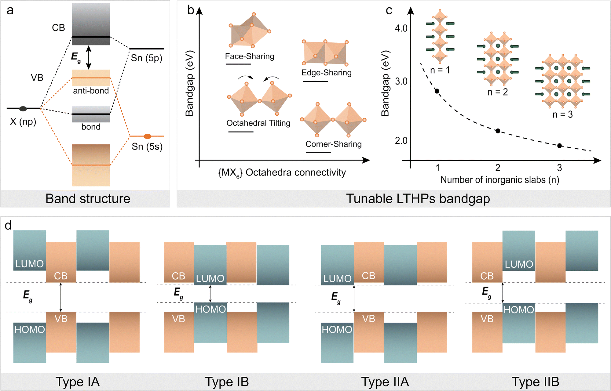 | ||
| Fig. 3 Optoelectronic properties of LTHPs. (a) Energy bandgap (Eg) of Sn halide (X) perovskites is defined by the Sn–X orbital interactions.68 (b) and (c) Illustration of the dependence of the Eg on (b) {MX6} octahedral connectivity and (c) number of inorganic slabs (n).24,44,50 Adapted with permission from ref. 31 Copyright 2022 Royal Society of Chemistry. (d) The representation of type I and type II quantum-well (QW) electronic structures based on the energy level alignments of conduction band (CB) minima, valence band (VB) maxima, highest occupied (HOMO) and lowest unoccupied (LUMO) frontier molecular orbitals. Adapted with permission from ref. 31 Copyright 2022 Royal Society of Chemistry. | ||
3. Synthesis methods
LTHPs can be accessed by various synthetic methods to achieve the materials with desired structural and optoelectronic characteristics. While Sn-based perovskites share the compatibility of fabrication methods with Pb halide perovskites, they also exhibit different crystallisation and growth dynamics, which require adaptation of the corresponding synthetic methodologies. This has so far involved solution-processing and solution-free processes (Fig. 4), which are effective for both 2D and 3D halide perovskites, as well as their mixed-dimensional perovskite heterostructures, as detailed below.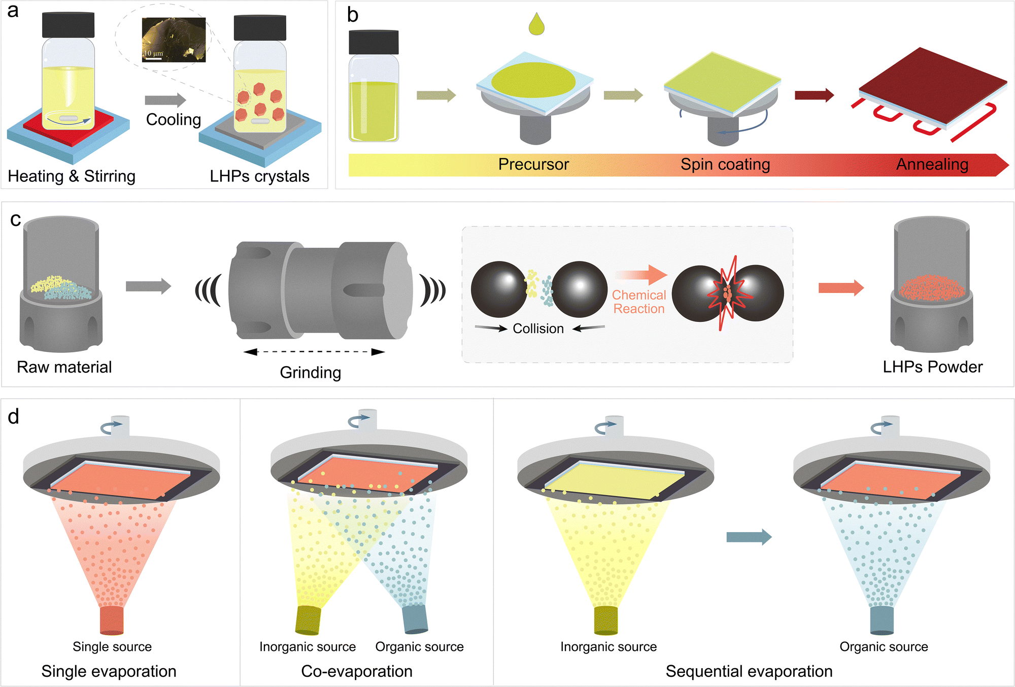 | ||
| Fig. 4 Synthetic methods for accessing layered tin halide perovskite materials. Schematic representation of (a) crystallisation, (b) spin-coating, (c) mechanosynthesis, and (d) thermal (co-/sequential) evaporation methods in the formation of layered Sn halide perovskite (LTHP) materials as single crystals (a), powders (b), and thin films (c) and (d). Adapted with permission from ref. 61 Copyright 2020 John Wiley and Sons. | ||
3.1 Solution-based methods
The preparation of LTHP materials often relies on solution-based methods, including the formation of single crystals and the corresponding thin films relevant to functional devices.The liquid-phase crystallisation of LTHPs often involves the use of hydrohalic acids (HI, HBr, and HCl) to synthesise single crystals (Fig. 4a).88 In conventional experimental conditions, the acid acts as a solvent for the starting materials (i.e., SnX2, organic spacer precursor, S, and A cation salt, AX) but also as a protonation and halide source (i.e., in the formation of SXx (x = 1–2)).13 The precursor materials are commonly dissolved in hydrohalic acid with heating and stirring, then cooled to room temperature to crystallise the desired material. This method enabled access to phase-pure crystals of LTHPs of different n values by adjusting the molar ratio of organic spacers and other starting materials. However, the exact stoichiometry of the resulting materials is not necessarily reflected in the stoichiometric ratio of precursors. If the organic spacer is not soluble enough, or the resulting LTHPs are less soluble, they will crystallise more readily and limit the phases with larger n values. Therefore, the exact ratio needs to be optimised, and it depends on the nature of the precursor components. Even for the same spacer cation, the solubility of LHPs in HX is different for Sn or Pb-based materials. For example, Kanatzidis et al. synthesised a homologous 2D (BA)2(MA)n−1SnnI3n+1 LHPs series (n = 1–5) using a stoichiometric reaction of SnCl2·2H2O, MAI, and BAI in excess HI/H3PO2 solution, whereas half-stoichiometric concentrations of BAI were suitable for the synthesis of Pb-based LHPs.44 Conversely, Song et al. synthesised (BEA)FAn−1SnnI3n+1 LTHP series (n = 1–3) using stoichiometric molar ratios of BEAI, FAI, and Sn(Ac)2 in HI/H3PO2 solution.61 Similarly, Zimmermann et al. synthesised 2D LTHPS of Bn2SnI4 (Bn = benzimidazolium) and BdiSnI4 (Bdi = benzodiimidazolium) composition by reacting SnI2 with the stoichiometric amounts of the corresponding organic salts in concentrated hydroiodic acid.55 However, Liang et al. first prepared 3AMPY·2HI powders by reacting 3AMPY with HI in a molar ratio of 1![[thin space (1/6-em)]](https://www.rsc.org/images/entities/char_2009.gif) :2. Subsequently, 3AMPYSnI4 crystals were synthesised by adding SnCl2 and 3AMPY·2HI powders, in a molar ratio of 1:1, to a mixture of 57% w/w aqueous HI solution and 50% aqueous H3PO2.52 This yielded phase-pure LTHPs, with insights into their crystal structure. In addition to using SnI2, Mora-Seró et al. demonstrated the synthesis of LTHPs using SnO as a precursor and successfully prepared (4FPEA)2SnI4 employing this method.89 The process utilized acetic acid as the solvent, which plays a key role in forming a hydrophobic layer on the perovskite surface. This protective network helped shield the material from moisture, thereby enhancing the stability under ambient conditions and in inert atmospheres over extended periods. Such LTHP crystals can also be used to form perovskite thin films in functional devices.
:2. Subsequently, 3AMPYSnI4 crystals were synthesised by adding SnCl2 and 3AMPY·2HI powders, in a molar ratio of 1:1, to a mixture of 57% w/w aqueous HI solution and 50% aqueous H3PO2.52 This yielded phase-pure LTHPs, with insights into their crystal structure. In addition to using SnI2, Mora-Seró et al. demonstrated the synthesis of LTHPs using SnO as a precursor and successfully prepared (4FPEA)2SnI4 employing this method.89 The process utilized acetic acid as the solvent, which plays a key role in forming a hydrophobic layer on the perovskite surface. This protective network helped shield the material from moisture, thereby enhancing the stability under ambient conditions and in inert atmospheres over extended periods. Such LTHP crystals can also be used to form perovskite thin films in functional devices.
The common method for LTHPs films is solution processing by using organic solvents (Fig. 4c). For this purpose, the precursor solution is prepared by mixing stoichiometric amounts of metal halides and ammonium halide (X) salts. For LTHPs, the Sn halides (SnX2) and organic spacer salts (SX2, x = 1–2) are mixed in organic solvents according to specific molar ratios. The solvents are typically polar, capable of dissolving both organic and inorganic salts, such as N,N-dimethylformamide (DMF) and dimethyl sulfoxide (DMSO), or a mixture of the two. However, since DMSO can enhance the oxidation of Sn(II),90 Abate et al. proposed a DMSO-free solvent system based on a mixture of dimethylpropyleneurea (DMPU) and N,N-diethylformamide (DEF) for Sn-based perovskites.91 The perovskite precursor solution can form films by relying on solution deposition methods, such as spin-coating, dip coating, and blade coating, with or without antisolvents (i.e., orthogonal solvents that induce crystallisation in the films). Loi et al. suggested that solution-processing of Sn perovskites with an antisolvent resulted in higher order and orientation due to the increased nucleation rate and crystallisation upon antisolvent injection.67 Furthermore, Kang et al. investigated the role of evaporation rate on Sn perovskite films through antisolvent engineering, where toluene was found to form the best-quality films.92 The corresponding crystallisation kinetics can be further controlled toward optimising the LTHP film quality.
The crystallisation kinetics of Sn halide perovskites generally follows classical theory, yet exhibits unique characteristics due to the distinct properties of Sn.93 Following the classical LaMer mechanism, the crystallisation process from solution can be divided into three stages associated with the variation of precursor solution concentration with time. In the first stage, the precursor concentration increases because of the solvent evaporation until it reaches the condition of nucleation. Nucleation is driven by supersaturation of the solution, and a nucleus that forms must overcome the Gibbs thermodynamic energy barrier to grow. The third stage, crystal growth, occurs as monomers diffuse from the solution to the surface of atomic nuclei, subsequently integrating into the perovskite lattice. The surface diffusion of the monomers and the reaction rate on the surface of the nucleus are two major factors limiting crystal nucleus growth in the process. In Sn perovskites, the surface reaction is rapid due to low Lewis acidity, resulting in diffusion-controlled growth. Consequently, the crystal growth terminates when the precursor concentration is too low. However, 3D Sn perovskite films obtained by easy solution processing often exhibit poor film quality due to the high Lewis acidity of Sn2+. This complicates the crystallisation of Sn perovskite films, as Sn2+ readily interacts with electron-donating species like FAI and MABr. Delgado et al. highlighted that the strong interaction between Sn2+ and iodide ions in FAI stabilises transition states and lowers activation energy, leading to rapid reactions.94 Loi et al. found two crystallisation stages in 3D Sn perovskite processing: initial surface and bulk crystallisation, followed by secondary crystallisation at grain boundaries. In contrast, 2D Sn perovskite films were suggested to exhibit a single crystallisation stage, starting at the air-solution interface and proceeding top-to-bottom. The slower crystallisation in the 2D films is attributed to the presence of organic spacers, which suppress supersaturation in the bulk of wet films and decelerate the diffusion-controlled growth.27,67 As a result, solution processing can yield a relatively pure n = 1 2D phase but cannot guarantee a pure phase for n > 1 compositions. Kanatzidis et al. attempted to synthesise the (BA)2(MA)3Sn4I13 phase with nominal n = 4 composition and easy solution processing, yet the XRD analysis of the films indicated a mixture of n = 2 and n = 3 phases.44 Even in the case of nominal n = 2 composition, the starting materials (SnI2, MAI, and BAI) in DMF formed only solvated ions, which crashed out kinetically due to low solubility and shifted the equilibrium to produce a mixture of phases upon spin coating.44 Loi et al. also found that nominal n = 4 and n = 8 samples also contained n = 2 phase and other co-existing phases.67 Single-phase films with higher n values can be grown using precursor solutions of “pre-synthesised” single-phase perovskites.44 Kanatzidis et al. also revealed that the solvent used to dissolve them affects film growth, e.g., DMSO stimulated parallel growth to the substrate, while DMF resulted in perpendicular growth.44 Such crystals are assumed to act as “crystal seeds”, which uniformly promote thin film growth into the desired phase.
3.2 Solvent-free methods
There has been an increasing interest in developing solvent-free approaches for LTHPs as environmentally friendly alternatives, including mechanosynthesis and thermal evaporation.Mechanosynthesis is a solvent-free method (Fig. 4c) that involves solid-state powder reactions using mechanical forces through milling, such as grinding or ball milling. This technique relies on uniformly mixing and grinding the starting materials in stoichiometric ratios over a certain period of time, typically in a solvent-free environment. The critical factors in controlling mechanochemical reactions include stoichiometric ratios, grinding time and intensity, milling atmosphere, and post-synthesis annealing. A significant advantage of this method is that it is not limited by the solubility of the spacer.13 Zhu et al. prepared 2D n = 1 RP (FBNA)2SnI4 and DJ (FPDMA)SnI4 by ball milling stoichiometric amounts of SnI2 and intended spacers. The obtained powders were further dissolved and deposited as thin films by spin-coating. Compared with thin films prepared by direct solution processing, films prepared by mechanosynthesis exhibited enhanced crystallinity.59 The pre-synthesised LTHP powders serve as 2D crystal seeds in solution. However, the mechanosynthesis is less explored in accessing LTHPs, while Pb-based layered perovskite of n > 3 compositions have not yet been synthesised using this approach. Further investigation is thereby needed to enable future applications in materials and devices, such as toward phase-pure 2D phases.
Thermal evaporation is another environmentally friendly and non-toxic deposition method that does not require organic solvents, such as DMF or DMSO.95–97 For the solution processing method, the precursor materials are typically dissolved in organic solvents, and the Sn perovskite films form during solvent evaporation. Instead, for thermal evaporation, materials are heated to specific temperatures, causing them to vaporise and travel through the low-pressure chamber toward the substrate, where the aggregation enables the formation of perovskite films.98,99 Crystallisation on the substrate follows comparable film growth mechanisms, including the so-called Volmer–Weber (island growth), Frank–van der Merwe (layer growth), or Stranski–Krastanov (layer-island growth) modes.98 In photovoltaic device architectures explored to date, the substrate lattice creates a mismatch with the perovskite lattice. Due to the weak binding force between the vapour precursor and the substrate, perovskite film growth primarily follows the Volmer–Weber island growth mode. Specifically, initially formed islands (nuclei) grow into grains, determining the final grain size and film morphology. Several key parameters influence the nucleation and growth process, including temperature, evaporation rate, vacuum, and substrate.95 The low melting points of common precursor materials, such as MAI, FAI, SnI2, and prospective organic spacer precursors, like PEAI, make vapor deposition a suitable choice for preparing Sn perovskites and LTHP films.100,101 Thermal evaporation offers advantages to solution processing, such as uniform film morphology, better thickness control, and easy multilayer film formation. Various methods have been successfully developed for depositing perovskites through thermal evaporation, such as co-evaporation,102,103 sequential deposition,103–105 and single-source evaporation (Fig. 4d). For instance, Qi et al. deposited MASnBr3 films using co-evaporation and sequential evaporation.103 in the case of co-evaporation, MABr and SnBr2 were deposited at a ratio of 4:1. For the sequential evaporation, a 100 nm layer of SnBr2 was deposited on TiO2/FTO followed by deposition of a 300 nm MABr layer. Such sequential deposition was proven more promising for Sn perovskite film quality due to the lower reaction speed, yet the obtained films still exhibited a higher concentration of defects. Different strategies have been used to overcome this challenge to date. For instance, Kanatzidis et al. improved the charge transport with a “multichannel interdiffusion” protocol,106 whereas Li et al. improved the quality of CsSnI3 films with an additive, thiosemicarbazide.107 The additive only served as a passivator and did not show evidence of improved crystallisation process. Other reports showed effective thermal deposition of 2D Sn perovskite films of (BA)2SnI4 and (PEA)2SnI4, yet these have not been applied in devices so far.108,109 To this end, the development of LTHPs still lags behind the research on other low-dimensional perovskites. While LTHPs have not been shown to influence the nucleation and crystallisation during thermal evaporation, they present a promising strategy for fabricating 2D/3D heterostructures with thermal evaporation. LHPs can serve as templating layers offering better lattice matching during thermal evaporation. This is especially relevant for enhancing the functionality of LTHPs that involve limited spacer solubility, which can advance their practical application.
4. Application in photovoltaics
LTHPs have stimulated increasing interest in photovoltaics in recent years, which primarily arises from the effort to replace Pb and the higher operational stability compared to their 3D counterparts.11 Moreover, LHPs have shown potential in regulating the crystallisation process of Sn perovskites in solution processing, and hold the promise to fabricate 2D/3D heterostructures using thermal evaporation or indirect fabrication methods, contributing to the formation of high-quality tin perovskite films for photovoltaics.8 The organic spacer plays a pivotal role in the structure and morphology of the resulting material, passivating defects, and offering enhanced resilience against environmental factors, such as moisture and oxygen, and suppressed ion migration,49 stimulating more research. The application of LTHPs in photovoltaics has been based on three distinct structures (Fig. 5a–c): LHP (2D), quasi-2D, and 2D/3D heterostructures.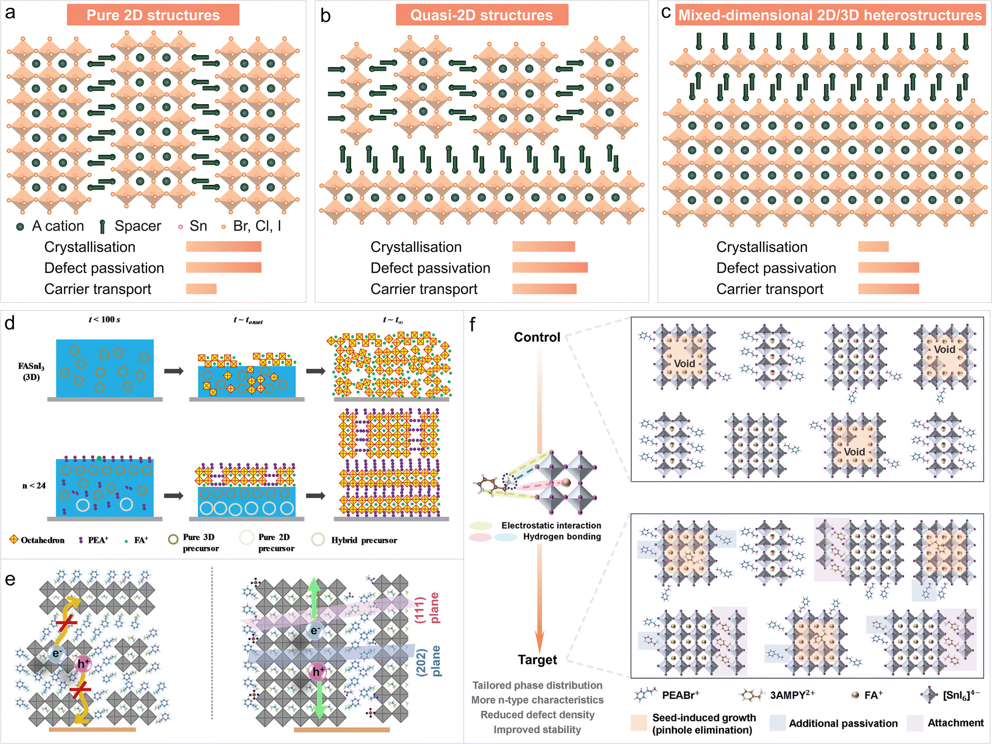 | ||
| Fig. 5 Application of LTHPs in photovoltaics. LTHPs were used in perovskite solar cells based on three types of distinct structures, namely (a) pure 2D structures, (b) quasi-2D phases, and (c) mixed-dimensional 2D/3D heterostructures. (d) Templating effects in mixed-dimensional Sn perovskite compositions. Reproduced from ref. 67 under a Creative Commons (CC-BY) license. (e) The effect of orientation on charge extraction in mixed-dimensional heterostructures. Reproduced from ref. 116 with permission. Copyright 2022 Elsevier. (f) Crystallisation control through targeted noncovalent interactions and passivation in mixed-dimensional Sn perovskite materials. Reproduced from ref. 52 with permission. Copyright 2024 John Wiley and Sons. | ||
While the 2D phases refer to pure-phase LHP structures, quasi-2D structures include those with mixed-dimensional (i.e., 2D/3D) phases, obtained mostly through solution processing. Finally, 2D/3D heterostructures refer to the stacking of 2D phases onto 3D layers to maximise photovoltaic performance.
4.1 Pure 2D LTHP photovoltaics
In LTHP film formation, only n = 1 compositions are regarded as pure 2D phases, as the higher (n > 1) compositional representatives typically involve mixed (n) phases. There have been efforts to access and understand the behaviour of pure-2D Sn perovskite structures by various techniques, from growing single crystals to solid-state powders and thin films.In 2018, Chen et al. prepared DJ Sn perovskite films of (4AMP)(FA)n−1SnnI3n+1 composition.51 They fabricated the films based on hot-casting, which involves dripping the precursor solutions onto pre-heated glass substrates. As the number of inorganic layers (n) increased from 1 to 4, the dimensionality of the perovskite crystal structure changed from pure (n = 1) phase to mixed (n) phases. The pure n = 1 (4AMP)SnI4 devices obtained a high VOC of 0.80 V but a low power conversion efficiency (PCE) of 2.15%, primarily due to the limited charge transport through the spacer barrier.51 The change in the composition (n > 1) could increase the photovoltaic performance, yet it was associated with the mixture of (n) phases, as well as the contribution of co-existing 3D phases. To improve the performance of pure 2D phases, in 2019, Zimmermann et al. introduced a benzimidazole (Bn) spacer cation in 2D RP Bn2SnI4 (n = 1) solar cells by solution processing.55 The material featured a narrower band gap (1.81 eV) compared to traditional ammonium-based spacers due to minor distortions in inorganic slabs, indicating good light absorption in the visible range. Bn2SnI4 still exhibited lower conductivity than 3D FASnI3, suggesting limited self-doping from oxides and vacancies. Nonetheless, Bn2SnI4 solar cells achieved a PCE of up to 2.3%, and the organic cations in the LHPs provided protection against moisture and oxygen, slowing Sn2+ oxidation.55 Similarly, benzodiimidazolium (Bdi) was used as a DJ spacer to form 2D DJ BdiSnI4 perovskites, which showed reduced band gap (1.80 eV) and inhibited Sn2+ oxidation due to symmetric HB that remains to be applied in solar cell devices.55 In 2021, Febriansyah et al. developed a ditopic organic dication 1-(2-ammonioethyl)-1H-imidazol-3-ium (ImEA2+) to template the 2D tin iodide perovskite of (ImEA)SnI4 composition. The resulting LTHPs exhibited short I⋯I contacts between their inorganic layers (4.174 Å), which is among the shortest ever recorded for LTHPs. The resulting devices exhibited an incident photon-to-current of up to 70% and a PCE of 2.26%,63 showcasing the impact of spacer and DJ phases in photovoltaics.
To obtain higher-n single-phase 2D perovskite films, it is possible to rely on single-phase perovskite crystals as precursors for solution processing.44 The LHP crystals can be pre-synthesized by liquid phase crystallisation or solid-state synthesis. These pre-synthesized bulky LHPs are assumed to leave molecular “LHPs crystal seeds” dissolved in organic solvents, which uniformly promote film growth in the phase. In 2017, Kanatzidis et al. deposited pure 2D RP films using bulky (BA)2(MA)n−1SnnI3n+1 (n = 1–5) LTHPs that were pre-synthesized by liquid phase crystallisation. They revealed that the solvent used to dissolve pre-synthesized LTHPs affects film growth, as DMSO results in parallel growth, while DMF results in perpendicular growth to the substrate.44 These LTHPs films were incorporated into solar cells and demonstrated PCE of 2.5% from films of n = 3 composition. Encapsulated devices retained more than 90% of the initial performance after 60 days, and lost just half of their performance after 4 months. Moreover, LTHP perovskite solar cells outperformed their 3D analogs in operational stability.44 Similarly, in 2020, Song et al. synthesised DJ LTHPs (BEA)FAn−1SnnI3n+1 (n = 1–3) phases by liquid phase crystallisation and subsequent deposition of thin films. The resulting (BEA)FA2Sn3I10 films exhibited a charge transfer time of 0.36 ps and carrier diffusion lengths over 450 nm for electrons and 340 nm for holes. Consequently, solar cells fabricated with these films achieve a PCE of 6.43% and a negligible hysteresis and retain over 90% of their initial PCE after 1000 h under N2.61 This highlights the potential of phase-pure LTHPs in solar cells.
The main limiting factors in the performance of pure LTHPs are their narrower absorption, stronger exciton binding energy, and inhibited charge transport across organic planes, which collectively hinder their power conversion efficiency (Fig. 5a). This limits the thickness of the layers, as charge recombination becomes predominant in thicker samples. However, thinner films lead to insufficient light absorption, and higher n values are preferred for better conductivity, yet such materials are difficult to access and tend to form mixed-dimensional phases.
4.2 Quasi-2D LTHP photovoltaics
Most LTHPs used in photovoltaics are quasi-2D systems that involve higher compositional (n > 1) representatives in a bulk mixture of (n, 2D/3D) phases as active layers for solar cells. They face challenges, such as rapid crystallisation and the susceptibility of Sn to oxidation, leading to high self-p-doping and excessive defects in the perovskite films. These issues result in low-quality Sn perovskite films, hindering the development of Sn-based perovskite photovoltaics. In this regard, introducing LHPs into Sn-based perovskite film can improve the crystallisation process and further offer stabilization (Fig. 5b).Loi et al. studied crystallisation dynamics to understand the impact of LHPs for achieving high-quality quasi-2D Sn perovskite films (Fig. 5d).67 A transition from 3D growth mode to 2D growth mode was observed when varying amounts of LTHPs were added to the 3D solution. Sn perovskite films with smaller amounts of organic spacer (e.g., leading to nominal n ≥ 24 compositions) exhibited 3D-like phases with enhanced orientation, as evidenced by the substitution of isotropic diffraction rings with diffraction arcs in the grazing-incidence wide-angle X-ray scattering (GIWAXS) patterns. In these quasi-3D films, bulk crystallisation remained significant, with randomly oriented crystals growing from the precursor solution. When the amount of organic spacer was increased, detectable LTHP phases with high n values could be observed in quasi-2D films. Unlike the heterogeneous nucleation involving two distinct stages in 3D Sn perovskites, quasi-2D films revealed single-stage nucleation and crystallisation. For nominal n ≤ 8, bulk crystallisation was largely suppressed, and the predominant process was the heterogeneous growth of 3D nuclei at the air/solution interface, resulting in oriented crystals. The 2D phase formed after the 3D crystallisation was complete, in contrast with the assumed 2D templating effect.67
Many organic cations were used in quasi-2D LTHP solar cells (Table 1). In 2018, Liu et al. studied the effects of alkyl chain length in devices based on nominal n = 4 LTHP compositions using n-butylammonium (BA), n-octyammonium (OA), and n-dodecylammonium (DA) iodide.46 The distribution of LTHP phases with shorter alkylamines was more ordered with preferred orientation compared to those with longer chains. The champion devices with a nominal n = 4 composition of BA2FA3Sn4I13 achieved an efficiency of 4.04%. Qiu et al. further studied the crystallisation kinetics of the same compound (BA2FA3Sn4I13) by using a co-solvent with a polar aprotic solvent (DMSO) and ionic liquid, methylammonium acetate (MAAc).70 This resulted in the formation of high-quality perovskite films and solar cell devices with a PCE of 4.03% and outstanding stability in the N2 atmosphere for 94 days.69 To further improve this performance, Diau et al. investigated the effect of 1,2-ethylenediammonium iodide (EDAI2) in BAI-based quasi-2D Sn perovskite films. They found that adding BAI significantly altered the orientation of crystal growth and improved the connectivity of the crystal grains, while pinholes were apparent on the surface of the pristine 3D FASnI3 films. The addition of 1% EDAI2 was found to remove pinholes and passivate the surface defect states, while preventing Sn2+/Sn4+ oxidation and inducing slow relaxation of the crystal structure. The champion device attained the best initial efficiency, 7.4%, which increased to 8.9% after a storage of 60 days.69 The utility of such bifunctional cations was also explored by Yuan et al., who developed novel LTHPs using 5-AVA while introducing NH4Cl as an additive,47 which led to vertically oriented quasi-2D films and solar cells with a PCE of up to 8.71%. The method was shown to be more universal with various spacers. Similarly, Liu et al. incorporated ALA cations into FASnI3 to form quasi-2D LTHPs.71 This compositional modification significantly improved the crystallinity and morphology of the perovskite films, resulting in a preferred crystal orientation that enhances charge carrier transport. After optimisation, a planar p–i–n photovoltaic device based on nominal n = 25 compositions achieved a maximum PCE of 9.48% with improved stability.71 Further attempts to rely on such tailored spacers with different alkyl chain lengths, such as HEAI40 and EAI,38,62 led to unexpected outcomes, as despite the ability to form quasi-2D phases, the spacers were found to incorporate into the 3D perovskite lattice. This stimulates other strategies on quasi-2D systems.
To this end, aromatic spacers were used in LTHP solar cells. The archetypical aromatic spacer cation is 2-phenylethylammonium (PEA). In 2017, Ning et al. first introduced PEA into Sn perovskites to form quasi-2D films to show that 2D LHPs with small n values were preferentially located at the bottom of the films.26 They found that PEA reduced defects and directed crystal orientation, resulting in highly oriented, dense, and smooth LTHP films with efficient charge carrier transport and enhanced stability. In particular, PEA cations could passivate undercoordinated Sn sites at the perovskite crystal surface and grain boundaries, whereas their 2D structure enhances resilience to oxygen and moisture, while suppressing ion migration. The resulting solar cells achieved a PCE of 5.94%, and unencapsulated devices maintained the efficiency in N2 atmosphere over 100 h.26 In 2018, Loi and co-workers optimised the approach to obtain higher quality LTHP films with superior crystallinity and a well-defined orientation by adding a small amount of LTHP to 3D Sn perovskite.27 Improved order and packing of crystal planes enhanced the robustness of the structure, reducing Sn vacancies. The resulting perovskite solar cells achieved a PCE of 9.0% with higher resistance to light illumination and external environmental factors. These representative examples have demonstrated the promise of PEA-based LTHPs and sparked further research aiming at improving performance and stability.
One key factor in achieving high performance is the orientation of LTHP films on the substrates. The alignment of inorganic slabs within each 2D perovskite grain is anisotropic, affecting charge transport along different crystallographic axes. The three principal orientations – (100), (110), and (111) – differ in their impact on vertical and in-plane charge conduction.33,110 The (100) orientation favors in-plane charge transport with limited vertical movement, while the (110) orientation enhances vertical connectivity and charge extraction despite some in-plane resistance. The (111) orientation is most beneficial for efficient charge conduction, as it facilitates strong vertical charge transport due to the optimal alignment of octahedral layers. This minimises barriers to vertical conduction, enhancing charge extraction and overall device efficiency. For example, Li et al. used PEACl as an additive and employed in situ GIWAXS measurements to investigate the influence of crystal orientation.111 They discovered that the (h00) diffraction peak intensity in FASnI3:PEACl films gradually decreased as the annealing temperature increased. At an optimized temperature of 100 °C, the film exhibited a well-defined quasi-2D structure with the (111) plane oriented perpendicular to the substrate surface, indicative of favorable vertical alignment. This optimisation led to the formation of highly crystalline, vertically oriented LTHPs, resulting in a PCE of 9.1%. Additionally, it was shown that PEA introduced a barrier layer at the surface, protecting the film from oxidation. These findings have stimulated more research efforts toward controlling 2D perovskite crystallisation to enhance efficiency and stability.
Other strategies were investigated to further control the crystallisation process of PEA-based quasi-2D LTHPs. One involves mixing PEA spacers with aliphatic cations, such as the commonly used BA. In 2019, Wei et al. first introduced the mixed spacer strategy to further control the crystallisation and achieved an efficiency of 8.82% with nominal n = 4 quasi-2D RP films using BA and PEA.74 They discovered that the intermediate phase hindering homogeneous and ordered crystal nucleation was effectively suppressed, resulting in high-quality film morphology and improved orientation. Furthermore, Öz et al. reported blade coating of Sn-PSCs mini-modules, where a combination of PEA and BA was needed for controlling the crystallisation. The dual-spacer strategy allowed fine control over crystallisation kinetics during the blade-coating process, suppressing undesirable phase segregation and enabling vertical orientation of perovskite layers, which is critical for efficient charge transport. The resulting devices exhibited high fill factors, low trap densities, and significantly improved stability under ambient conditions.112
In addition to spacer cations, additive engineering has proven effective in regulating the crystallisation behavior. While several studies have reviewed additives mainly used for passivation or as reducing agents,113,114 additives specifically aimed at improving the crystallisation of quasi-2D LTHPs are limited. Apart from conventional ammonium cations, one typical group of additives involves pseudohalogen regulators. In 2018, Ning et al. introduced NH4Cl to grow 2D/quasi-2D/3D Sn heterostructures. Such a hierarchical structure of perovskite films achieved a PCE of up to 9.41% and retained 90% of its initial performance for almost 600 h.73 Efforts to optimise the device structure have further increased the efficiency to over 10%.75,77 Next, Hao and co-workers developed a facile and effective strategy to deposit quasi-2D Sn perovskites with 15 mol% PEA-SCN.82 The SCN− ions hindered Sn2+ oxidation by modulating the coordination and crystal growth of perovskite films. These interactions suppressed the nonradiative charge recombination, and the resulting devices achieved efficiencies of 12.88% with a VOC of 863 mV and high stability, retaining performance for over 2000 h under a N2.82 PEA-SCN was also shown to form quasi-2D LTHPs.115 Finally, ionic liquids have also been employed as additive-regulators to improve the crystallisation. A typical example is BAAc, the acetate form of BA, which functions as an ionic liquid. In 2021, Chen et al. also used nominal n = 4 quasi-2D films with PEAI and either BAI or BAAc separately.78 Compared to the BAI, the BAAc interacted strongly with A cations and Sn2+, allowing the formation of controllable intermediates for the favourable growth of smooth, dense, and highly oriented films. While BAI achieved a PCE of 7.16%, BAAc reached a PCE of 10.36%, along with improved stability, retaining approximately 90% after around 600 h of storage in a N2 atmosphere without encapsulation.78 Abate et al. introduced BAAc into quasi-2D Sn perovskite inks prepared from PEABr and EABr. The BAAc ionic liquid was shown to affect the Sn through O⋯Sn coordination and N–H⋯X HB. These interactions effectively retarded crystallisation and provided more uniform nucleation sites, resulting in compact quasi-2D films with preferential crystal orientation. The resulting solar cells achieved a PCE of 10.4%, retaining 96% of their initial efficiency after over 1000 h of aging. The thermal stability at 85 °C was also demonstrated, maintaining 80% of their initial efficiency (T80) over 400 h.81 Furthermore, PEA spacers could also be functionalised to serve as ionic liquids. In 2022, Q. Yu et al. proposed a mixed pseudo-halide ionic liquid engineering approach by using acetate (Ac−) and BF4− anions to make quasi-2D LTHPs of PEA2FA4Sn5I16 composition. It was found that the mixed Ac− and BF4− anions promoted homogeneously distributed PEA cations in the precursor by breaking the PEA⋯PEA stacking, consequently retarding the crystallisation orientation by coordinating SnI2 (Fig. 5e). A prominent efficiency of 8.9% was achieved for nominal n = 5 RP compositions, which retained 80% of the initial efficiency for 400 h in a N2-filled glovebox without encapsulation.116 Beyond the discussed ionic liquids such as MAAc,70 BAAc,78,81 PEAAc, and PEABF4116 in LTHPs, other ionic liquids like 1-butyl-3-methylimidazolium bromide (BMIBr),117 formamidine acetate (FAAc),118 and methylamine formate (MAFa)119 have demonstrated effectiveness in 3D Sn perovskites. While not yet explored in layered systems, these ionic liquids present promising candidates for future studies toward enhancing film quality and device performance. Many other reports have since relied on PEA-based quasi-2D Sn perovskite films with comparable additives for improved film quality and solar cell device performance, such as 4-phenylthiosemicarbazide (4PTSC)120 and cyanoacetohydrazide (CAH),121,122 among others, which could be applied to LTHPs.
Aromatic spacers with thiophene rings have also been extensively studied to improve the crystallisation in Sn perovskites. In 2022, Song and co-workers first introduced 2-thiopheneethylammonium iodide (TEAI) into MASnI3 perovskite precursor, obtaining quasi-2D films with preferred orientation and a low Sn4+ concentration. The perovskite solar cells showed a PCE of 6.8%, amongst the highest reported for MASnI3 solar cells.53 In the following year, Wang and co-workers investigated how the competition between intra- and intermolecular interactions regulates the sol-to-gel transition process in LTHPs by preparing nominal n = 4 quasi-2D films using either benzylammonium (BNA or BE) or thiophene-methylammonium (TH) iodide.54 The devices of TH2FA3Sn4I13 composition attained a PCE of 9.03% while those made with BE2FA3Sn4I13 only reached a PCE of 4.04%. Compared to BNAI, which contains a benzene ring, THI with a thiophene ring weakened the intermolecular interactions between iodostannic sheets and spacer cations by strengthening the intramolecular interactions within the spacer layer. While some intermolecular attraction is essential for colloid formation, overly strong interactions can lead to aggregation and poor crystallinity. The competition between intramolecular and intermolecular interactions thus led to stronger electrostatic repulsion between charged colloids, further stabilising them and retarding sol–gel transition before crystal formation. The demonstration of this strategy provides a direction to effectively improve crystallisation quality with a wider processing window for order crystal growth of RP LTHPs.54
The intermolecular interactions between spacer cations were further tailored using fluorinated spacers that were proven effective in LTHPs due to their intrinsic dipole and intermolecular interactions. In 2021, He and co-workers introduced 4-fluoro-phenethylammonium bromide (FPEABr) into the LTHP precursor solution to fabricate quasi-2D tin-perovskite films and modulate their microstructure.60 The introduction of the 2D phase induced oriented growth of 3D FASnI3. In the optimal quasi-2D films, the 2D phase enveloped the 3D grains and was located at the surfaces and grain boundaries. This prevented the oxidation of Sn2+ and reduced defect density. The champion device achieved PCE of 14.81% (14.01% certified) with a 10% addition of FPEABr.60 However, there was a ‘vdW gap’ between adjacent spacers in RP phases.
Instead, DJ perovskites, where the inorganic sheets are directly connected by bifunctional spacers, can strengthen interlayer coupling and exhibit a more stable structure. The development of DJ quasi-2D films is more challenging and lags behind the RP phases, yet investments continue to realise their potential for improved stability and device performance. The first bifunctional spacer to be systematically studied for LTHPs is 4-(aminomethyl)piperidine diammonium (4AMP). In 2018, the work of Chen et al. relied on 4AMP in the nominal n = 4 (4AMP)(FA)3Sn4I13 films, showing reasonable absorption characteristics with the edge at 860 nm.51 The corresponding solar cell devices fabricated by hot casting achieved a promising PCE of 4.22%. Additionally, the PCE of non-encapsulated devices irradiated in a N2 atmosphere at 45 °C for 100 h was tracked, showing only a 9% initial PCE loss, indicating device stability.51 In 2024, Huang et al. developed DJ-phase quasi-2D Sn perovskites with 3-aminobenzylamine (3ABA) and 4-aminobenzylamine (4ABA) π-conjugated spacers for application in photovoltaics.56 3ABA exhibited a higher dipole moment of 7.52 D as compared to 4ABA (4.63 D). Consequently, the DJ quasi-2D LTHPs prepared by using 3ABAI2 precursors demonstrated rapid charge transfer and a low exciton binding energy of just 84 meV. Moreover, their salts (ABAI2) were partially replaced with diacetate (ABAAc2) to prolong the crystallisation time due to weaker acidity and slower reaction rate. The devices of nominal n = 5 (3ABA)FA4Sn5I16 films achieved a PCE of 6.81% and demonstrated stability for 840 h, with less than 5% degradation in a N2 atmosphere without encapsulation.56 To enable further improvement in performance, in 2025, Liang et al. synthesized 3-(aminomethyl)pyridinium (3AMPY) based (3AMPY)SnI4 crystals introduced into the PEA-contained LTHP perovskite precursor solution to optimise the crystallisation process and regulate the phase distribution.52 The strong coordination between 3AMPY and 3D perovskite components and the introduced (3AMPY)SnI4 nucleation sites effectively reduced the undesired 2D phase and increased the desired 3D phase content in the Sn-based perovskites, forming a high-quality film with low trap density and non-radiative recombination loss (Fig. 5f). 2D DJ slabs stabilised the perovskite structure by inhibiting oxidation of Sn2+ to Sn4+ and providing additional protection. The stabilised perovskite structure led to an increased PCE from 10.91% to 13.28%, retaining 96.0% of its performance for over 3000 h in a N2 atmosphere.52 Further investigations and applications of DJ Sn perovskites in solar cells are ongoing. For example, Yao et al. studied the structure, stability, and optoelectronic properties of a series of 1,4-phenyldimethylammonium (PDMA)-based DJ LTHPs for perovskite photovoltaics.123 It was shown that barriers may form due to imperfections in the stacking of the inorganic planes, which disrupt the conduction pathways and result in field-dependent charge collection. To achieve higher device performance, long-range vertical packing is essential to limit recombination and enhance charge conduction.11 Moreover, an alternative approach is to dope the spacers to help decrease the dielectric contrast and lower potential barriers. Other works show that certain spacers cannot form a 2D phase, but play a role in slowing down crystallisation and passivate defects.9,124 This is relevant for the broader understanding of mixed-dimensional structures and their control.
4.3 2D/3D LTHP heterostructures in photovoltaics
2D/3D perovskite heterostructures have been widely used in photovoltaics by relying on the 2D perovskite overlayer to stabilise the more effective 3D active layer for solar cells. In the quasi-2D films, the organic spacer cation plays a critical role in regulating crystallisation, yet controlling 2D distribution remains challenging. This affects charge transport and separation due to the quantum confinement and anisotropy of LHPs, leading to a compromise in device performance. Moreover, interfaces, such as the ones with charge-extraction layers, have been shown to significantly impact charge carrier transport and the photovoltaic performance. Compared with the disordered 2D structures in quasi-2D films, a targeted 2D interlayer can offer protection against ion migration and external factors while tailoring the interfacial band alignment. This makes the applications of LTHPs in 2D/3D heterostructures (Fig. 5c) relevant as compared to direct composition mixing in quasi-2D structures. There have been different approaches to achieving these structures in LTHPs for photovoltaics.Early 2D/3D heterostructures relied on a two-step process. In 2018, Wu et al. fabricated 2D/3D bulk heterojunction Sn-based perovskite solar cells using a two-step process.72 First, FAI was dissolved in poly(2,4-ethylenedioxythiophene (PEDOT:PSS) and spin-coated onto the substrate. Then, PEAI was evaporated on top of the FAI film, followed by the evaporation of SnI2, which reacted with FAI and PEAI to form the Sn perovskite. The evaporated PEAI attached both on and between FAI particles, enhancing surface coverage of both FAI and FASnI3 films. A small fraction of PEAI resulted in the formation of four phases: SnI2, FASnI3, (PEA)2(FA)n−1SnnI3n+1, and PEA2SnI4. Increasing the amount of PEAI led to the formation of a 2D/3D bulk heterojunction (PEA,FA)SnI3 film of FASnI3, (PEA)2(FA)n−1SnnI3n+1, and PEA2SnI4. The 2D/3D bulk heterojunction structure, combined with a LiF modification interlayer, resulted in a device that achieved a PCE of 6.98%, offering a promising perspective.72 Similarly, in 2020, Moon et al. fabricated a Sn-based perovskite 2D/3D heterostructure by a sequential vapour deposition.76 First, a uniform layer of SnI2 was deposited on the substrate through thermal evaporation. Next, PEAI was evaporated onto the SnI2-coated substrate at room temperature, maintaining the vacuum in the chamber. This led to the direct formation of a 2D PEA2SnI4 layer on the surface via reaction with SnI2, without requiring additional heat treatment. The substrate was then placed in a chamber containing MAI created by vaporising MAI powder. The MAI vapor diffused through the PEA2SnI4 perovskite layer and reacted with the remaining SnI2, resulting in the formation of 3D MASnI3. Such a sequential process ensured uniformity in the films and allowed for precise thickness control without harming the 3D layer. The introduction of the 2D overlayer suppresses Sn oxidation and enhances the crystallinity. A planar-type solar cell showed an average PCE of 9.2 ± 0.2%.76
Alternative interface treatment methods can also be used to construct 2D/3D heterostructures by converting the 3D perovskite to 2D perovskite by either using bottom or top surface treatment. The surface treatment typically involves adding a spacer to the antisolvent or using a spacer solution to treat the previously formed 3D Sn perovskite. It is important that the post-processed spacer solution has adequate solubility and does not significantly damage the 3D Sn perovskite layer, as this could degrade the performance of the material. Larger organic moieties, often based on ammonium anchoring groups, interact with surface A-cation vacancies through hydrogen bonding, forming molecular layers or 2D/3D interfaces.
In 2018, Gong et al. introduced an ultrathin LHP interlayer close to the PEDOT:PSS perovskite interface by bottom treatment.79 Specifically, PEABr solution in DMF was spin-coated onto the PEDOT:PSS-coated substrates, followed by FASnI3 precursor deposition. PEA was expected to partially or fully substitute FA in the 3D precursor and convert it into 2D perovskite, forming an ultrathin LTHP interlayer. Confirming the existence of the 2D phase was challenging due to the relatively weak reflection of the ultrathin LHPS interlayer, especially when compared to the thicker (∼500 nm) 3D perovskite films. The growth of perovskites near the interface was promoted, improving film morphology and reducing trap states. Effective trap passivation was enabled, significantly suppressing charge carrier accumulation and recombination in the device. As a result, a PCE of 7.05% was achieved, with stabilised power output and minimal hysteresis.79 Similarly, in the following year, He and co-workers employed PEABr to form an ultrathin LHPs on the surface of the FASnI3 interface with phenyl-C61-butyric acid methyl ester (PCBM) in the inverted planar device structure.80 PEABr surface treatment was conducted by PEABr solution in isopropanol spin-coated onto the FASnI3 perovskite film, followed by annealing at 100 °C to form an ultrathin overlayer. Although the 2D overlayer was thin, a 2D signal emerged in the XRD patterns of films treated with higher concentrations of PEABr. The PEABr-based 2D interlayer was further proven to reduce defect density, improve film morphology, and provide better band alignment with the electron-transport layer, while acting as a protective layer that preserved the perovskite from Sn2+ oxidation. This treatment enhanced device efficiency from 4.77% to 7.86% and improved stability, retaining 80% efficiency after 350 h, while control devices failed within 140 h.80 This strategy was proven effective by Huang et al. in 2023125 who introduced PEACl for post-treating FASnI3 films, forming a 2D/3D heterostructure, which was evidenced by XRD. This not only improved film morphology by eliminating SnF2 impurities but also induced preferred orientation, well-matched energy levels, and effective defect passivation. Consequently, FASnI3-based PEACl-treated devices achieved PCE of 11.63%.125
Surface post-treatments provide a versatile optimisation tool. In 2019, Hayase et al. introduced another post-treatment using 1,2-diaminoethane (EDA or DEA) in chlorobenzene. The peaks corresponding to the unreacted SnI2 significantly decreased, indicating the removal of unreacted SnI2 due to the chemical interaction with EDA. The VOC of devices increased up to 0.1 V, attributed to the passivation of surface defects, suppression of Sn oxidation, and stabilisation of undercoordinated Sn. By optimising the concentration of EDA, they enhanced the device performance from 8.09% to 9.37%, which further reached 10.18% after one-week storage.126 In 2020, the same group further optimised the A site cation substitution with EA for band-level engineering, achieving a high PCE of 13% when combined with EDA treatment.38
In addition, surface treatment can also be done via an antisolvent. In 2024, Li et al. applied a bifunctional spacer, PDMABr2, to fabricate 2D/3D Sn heterostructure films through this method.10 The diffraction peaks representing the quasi-2D phase of the PDMABr2-treated perovskite films remained until the completion of the annealing process. Strong interactions between PDMABr2 and the perovskite surface passivated uncoordinated Sn(II) and suppressed nonradiative recombination, improving electron transfer and stability against water and oxygen. As a result, the PDMABr2-treated device achieved a PCE of 11.44% and retained over 90% of its initial efficiency for 1000 h in a N2-filled glovebox, demonstrating high efficiency and stability. Additionally, it maintained over 90% of its original efficiency for more than 200 h in a 10% RH moisture N2 environment.10 Other solvents can play a critical role in the nature of the heterostructure and its device effectiveness.
In 2020, Han et al. reported a graded 2D/3D heterostructure achieved through post-treatment with bulky 4-(trifluoromethyl) benzyl ammonium cations (TFBA).83 The post-treatment involved dip-coating in the spacer solution rather than spin-coating. Specifically, the FASnI3 film, without thermal annealing, was dipped into TFBAI solution in chloroform for 10 s. TFBAI-treated perovskite films exhibited additional peaks assigned to the (100) and (200) crystal planes of the 2D TFBA2SnI4 perovskite, respectively. Further analysis indicated that the content of (TFBA)2SnI4 phase decreases gradually from the surface to the inner part of the perovskite layer. This heterostructure could selectively extract charge carriers at the electron-transport layer interface, resulting in the reduction of the density of trap states and suppression of the Sn oxidation. Consequently, a graded heterostructure increased the VOC by 120 mV and achieved a PCE of 11%. Furthermore, the optimised device demonstrated improvement in operational stability, maintaining a PCE of over 10% after 500 h of irradiation.83
The outcome of post-treatments is spacer-dependent (Table 1). In 2021, Diau et al. studied eight bulky ammonium spacers to form 2D/3D Sn perovskite heterostructures by post-surface treatment.45 Additionally, hexafluoro-2-propanol (HFP) was used as a solvent instead of isopropyl alcohol (IPA) to dissolve the spacers, such as BA, n-hexylammonium (HA), allylammonium (ALA), cyclohexylammonium (CHA), 2-phenylethylammonium (PEA), anilinium (AN), 2-fluorophenylethylammonium (2FPEA), and 2-fluoroanilinium (2F-AN). The Sn perovskite film was damaged by pure isopropanol within 20 s, but remained stable with HFP, which acted as an electron-withdrawing acid that interacts with spacers to slow the conversion of 3D FA0.8GA0.2SnI3 to a 2D overlayer. The formation of the 2D layer was confirmed using GIWAXS and other techniques. The n = 2 phase was the most favourable quasi-2D structure, but a large concentration of spacers can induce the formation of n = 1 phases, as observed in the PEA and 2FPEA case. Device power conversion efficiency (%) uon treatment with BA (9.1%), PEA (9.6%), AN (10.4%), ALA (9.3%), and 2F-AN (8.9%) outperformed the standard cell (8.7%), while those treated with HA (8.4%), CHA (7.8%), and 2FPEA (8.3%) performed slightly less efficiently. The champion AN-treated devices showed a remarkable PCE of 10.6% and demonstrated excellent stability in ambient air without encapsulation. The AN device also exhibited a self-healing effect while enduring light soaking under illumination and harsh thermal stress cycles between 20 and 50 °C for 10 cycles.45
In 2025, Zhu et al. demonstrated solvent-dependent deposition of perfluoroarene-based RP and DJ perovskite phases and the corresponding 2D/3D heterostructures.59 They relied on two perfluoroarene cations, 2-(perfluorophenyl)methylammonium (FBNA) and 1,4-(perfluorophenyl)dimethylammonium (FPDMA), to form RP and DJ LTHPs, respectively. They demonstrated the capacity to form 2D perovskites mechanosynthetically. Moreover, they were applied to FASnI3 perovskite solar cells by solution-processing from orthogonal solvents, identifying a solvent for film processing, 2-pentanol. While F-PDMA formed a 2D/3D heterostructure, F-BNA remained assembled as a molecular interlayer, resulting in a higher overall photovoltaic performance with PCE over 9% in inverted DMSO-free perovskite solar cell architectures with limited operational stability.59 These findings challenged the role of 2D overlayers in mixed-dimensional perovskite heterostructures for perfluoroarene-based on other related spacer cations, while emphasising the role of processing conditions such as the solvents. Moreover, the results emphasised the necessity to distinguish between the different modes of action of the organic spacer precursors, which, despite the capacity of forming 2D phases, could act as molecular modulators in the resulting solar cells. These efforts to understand the mechanisms, complemented by developing novel low-dimensional materials, offer a promising direction for advancing LTPH materials and their photovoltaics.
The methods to achieve 2D/3D heterostructures remain challenging in controlling the phase formation and their distributions, which relates to the crystallisation of Sn perovskites. While 2D layers can effectively passivate the interface, Sn vacancies and other defects persist in the 3D bulk and grain boundaries. The high density of Sn vacancies leads to non-radiative recombination, reduced carrier lifetimes, and lower device performance. These vacancies also disrupt the Sn–I framework and serve as sites for Sn2+ oxidation to Sn4+, promoting deep trap formation and degradation. If the 2D overlayer degrades and oxygen penetrates into the 3D phase, degradation may proceed rapidly. High-quality 3D perovskite films with low density of defects are essential for improving both performance and long-term stability. It would be desired to fabricate heterostructures by one-step solution processing while effectively regulating crystallisation and suppressing defect formation.70,72 However, the aggregation of intermediates poses barriers that prevent large 2D perovskite colloids from forming stable clusters, causing slower nucleation compared to their 3D counterparts. This difference in nucleation kinetics leads to undesirable 2D/3D phase distribution, known as quasi-2D structures. Recently, He et al. developed high-quality 2D/3D heterostructures of Sn perovskite thin films by introducing Cs+ to partially replace organic cations in the 2D Sn perovskite colloids, which reduced the colloid size and lowered the aggregation barrier.127 This reduced electrostatic repulsion and promoted the coagulation of 2D and 3D Sn perovskite colloids in the precursor solution for the growth of homogeneous 2D/3D heterostructures with reduced trap states. As a result, Cs-incorporated Sn perovskite devices achieved an excellent PCE of 17.13% (certified 16.65%) and exhibited stable operation under continuous illumination for over 1500 h in N2 atmosphere without encapsulation.127 This emphasises the importance of colloidal chemistry and crystallisation engineering of mixed-dimensional LTHP heterostructures, complementing prior reports in paving the way for high-performance, lead-free perovskite photovoltaics.
5. Summary and outlook
Layered tin halide perovskite materials have emerged as a promising alternative to toxic lead-based perovskites in photovoltaics. However, their instability during operation and limited device performance stimulate ongoing research activities to develop more effective tin-based materials and devices. This has involved extensive research on designing appropriate organic spacer cations and tailoring their functionality, as well as supramolecular assemblies, to address the pressing issues. Moreover, this effort has been coupled with the analysis of various 2D and mixed-dimensional perovskite compositions and synthetic techniques, including both solution-based and solvent-free (mechanosynthetic or thermal evaporation) methods, while analysing the characteristics of the resulting materials to enable their control in functional devices.Despite the rapid developments, challenges remain in understanding the mechanisms and the limited stability of tin perovskites, leading to inferior performances, especially for layered perovskite systems incorporating electronically insulating organic spacer cations. This provides opportunities to address some of these shortcomings by relying on the additional functionalities of organic spacer layers to control their assemblies, as well as their electroactivity, which remains to be exploited in tin-based layered perovskites. Toward this goal, the utility of photo/redox active or chiral organic agents might offer new dimensions for advancing optoelectronic characteristics. These new design elements, complemented by further developments in material preparation techniques and their structural and optoelectronic characterisation, promise to transform the use of tin-based perovskite materials in new-generation photovoltaics and related technologies in the future.
Author contributions
M. Z. has written the first draft of the manuscript with the support of J. V. M., who supervised her work. B. C. and A. M. supported the writing process under the supervision of M. S. and J. V. M. All authors have contributed to the manuscript writing and completion.Conflicts of interest
There are no conflicts to declare.Data availability
This is a review article, and all the data we refer to have been previously published. The schematics and illustrations are available upon request.Acknowledgements
M. Z. appreciates the CSC Fellowship, enabling her to pursue her doctoral studies in this research direction. J. V. M is grateful for support from the Swiss National Science Foundation (project no. 193174) and acknowledges the European Research Council Funding under the Horizon Europe Progam (SmartHyMat, Grant Agreement 101114653). M. S. acknowledges funding from the European Research Council under the Horizon Europe Program (LOCAL-HEAT, Grant Agreement 101041809). We appreciate the generous mentorship and support of Prof. Ullrich Steiner (Adolphe Merkle Institute, University of Fribourg) and Prof. Maria A. Loi (University of Groningen, The Netherlands) throughout this and other collaborative projects.References
- M. Pitaro, E. K. Tekelenburg, S. Shao and M. A. Loi, Adv. Mater., 2022, 34, 2105844 CrossRef CAS PubMed.
- E. Aktas, N. Rajamanickam, J. Pascual, S. Hu, M. H. Aldamasy, D. Di Girolamo, W. Li, G. Nasti, E. Martínez-Ferrero, A. Wakamiya, E. Palomares and A. Abate, Commun. Mater., 2022, 3, 1–14 CrossRef.
- M. Konstantakou and T. Stergiopoulos, J. Mater. Chem. A, 2017, 5, 11518–11549 RSC.
- D. H. Fabini, R. Seshadri and M. G. Kanatzidis, MRS Bull., 2020, 45, 467–477 CrossRef.
- F. Yang and K. Zhu, Adv. Mater., 2024, 36, 2314341 CrossRef CAS PubMed.
- D. Ricciarelli, D. Meggiolaro, F. Ambrosio and F. De Angelis, ACS Energy Lett., 2020, 5, 2787–2795 CrossRef CAS.
- H. Zhu, J. Ma, P. Li, S. Zang, Y. Zhang and Y. Song, Chem, 2022, 8, 2939–2960 CAS.
- J. Zhao, Z. Zhang, G. Li, M. H. Aldamasy, M. Li and A. Abate, Adv. Energy Mater., 2023, 13, 2204233 CrossRef CAS.
- Y. Shi, Z. Zhu, D. Miao, Y. Ding and Q. Mi, ACS Energy Lett., 2024, 1895–1897 CrossRef CAS.
- F. Yang, R. Zhu, Z. Zhang, Z. Su, W. Zuo, B. He, M. H. Aldamasy, Y. Jia, G. Li, X. Gao, Z. Li, M. Saliba, A. Abate and M. Li, Adv. Mater., 2024, 36, 2308655 CrossRef CAS PubMed.
- G. Grancini and M. K. Nazeeruddin, Nat. Rev. Mater., 2019, 4, 4–22 CrossRef CAS.
- S. Teale, M. Degani, B. Chen, E. H. Sargent and G. Grancini, Nat. Energy, 2024, 9, 779–792 CrossRef CAS.
- X. Li, J. M. Hoffman and M. G. Kanatzidis, Chem. Rev., 2021, 121, 2230–2291 CrossRef CAS PubMed.
- L. Mao, W. Ke, L. Pedesseau, Y. Wu, C. Katan, J. Even, M. R. Wasielewski, C. C. Stoumpos and M. G. Kanatzidis, J. Am. Chem. Soc., 2018, 140, 3775–3783 CrossRef CAS.
- B. Saparov and D. B. Mitzi, Chem. Rev., 2016, 116, 4558–4596 CrossRef CAS PubMed.
- J. V. Milić, J. Mater. Chem. C, 2021, 9, 11428–11443 RSC.
- Y. Gao, Z. Wei, S.-N. Hsu, B. W. Boudouris and L. Dou, Mater. Chem. Front., 2020, 4, 3400–3418 RSC.
- E. A. Katz, Helv. Chim. Acta, 2020, 103, e2000061 CrossRef CAS.
- L. Mao, C. C. Stoumpos and M. G. Kanatzidis, J. Am. Chem. Soc., 2019, 141, 1171–1190 CrossRef CAS.
- R. D. Willett, J. Chem. Phys., 1964, 41, 2243–2244 CrossRef CAS.
- Y. I. Dolzhenko, T. Inabe and Y. Maruyama, Bull. Chem. Soc. Jpn., 1986, 59, 563–567 CrossRef CAS.
- A. Kojima, K. Teshima, Y. Shirai and T. Miyasaka, J. Am. Chem. Soc., 2009, 131, 6050–6051 CrossRef CAS PubMed.
- Research-Cell Efficiency Chart, https://www.nrel.gov/pv/cell-efficiency.html, (accessed March 26, 2025).
- D. B. Mitzi, C. A. Feild, W. T. A. Harrison and A. M. Guloy, Nature, 1994, 369, 467–469 CrossRef CAS.
- T. M. Koh, T. Krishnamoorthy, N. Yantara, C. Shi, W. L. Leong, P. P. Boix, A. C. Grimsdale, S. G. Mhaisalkar and N. Mathews, J. Mater. Chem. A, 2015, 3, 14996–15000 RSC.
- Y. Liao, H. Liu, W. Zhou, D. Yang, Y. Shang, Z. Shi, B. Li, X. Jiang, L. Zhang, L. N. Quan, R. Quintero-Bermudez, B. R. Sutherland, Q. Mi, E. H. Sargent and Z. Ning, J. Am. Chem. Soc., 2017, 139, 6693–6699 CrossRef CAS PubMed.
- S. Shao, J. Liu, G. Portale, H.-H. Fang, G. R. Blake, G. H. ten Brink, L. J. A. Koster and M. A. Loi, Adv. Energy Mater., 2018, 8, 1702019 CrossRef.
- Z. Chen, J. J. Wang, Y. Ren, C. Yu and K. Shum, Appl. Phys. Lett., 2012, 101, 093901 CrossRef.
- N. K. Noel, S. D. Stranks, A. Abate, C. Wehrenfennig, S. Guarnera, A.-A. Haghighirad, A. Sadhanala, G. E. Eperon, S. K. Pathak, M. B. Johnston, A. Petrozza, L. M. Herz and H. J. Snaith, Energy Environ. Sci., 2014, 7, 3061–3068 RSC.
- W. Liao, D. Zhao, Y. Yu, C. R. Grice, C. Wang, A. J. Cimaroli, P. Schulz, W. Meng, K. Zhu, R.-G. Xiong and Y. Yan, Adv. Mater., 2016, 28, 9333–9340 CrossRef CAS PubMed.
- W. Luo, G. AlSabeh and J. V. Milic, in Photochemistry, ed. S. Crespi and S. Protti, Royal Society of Chemistry, Cambridge, 2022, vol. 50, pp. 346–370 Search PubMed.
- N. Mercier, Angew. Chem., Int. Ed., 2019, 58, 17912–17917 CrossRef CAS.
- Y. Chen, Y. Sun, J. Peng, J. Tang, K. Zheng and Z. Liang, Adv. Mater., 2018, 30, 1703487 CrossRef PubMed.
- J.-C. Blancon, J. Even, C. C. Stoumpos, M. G. Kanatzidis and A. D. Mohite, Nat. Nanotechnol., 2020, 15, 969–985 CrossRef CAS PubMed.
- V. M. Goldschmidt, Naturwissenschaften, 1926, 14, 477–485 CrossRef CAS.
- L. Mao, Y. Wu, C. C. Stoumpos, B. Traore, C. Katan, J. Even, M. R. Wasielewski and M. G. Kanatzidis, J. Am. Chem. Soc., 2017, 139, 11956–11963 CrossRef CAS PubMed.
- S. Shao, J. Dong, H. Duim, G. H. Ten Brink, G. R. Blake, G. Portale and M. A. Loi, Nano Energy, 2019, 60, 810–816 CrossRef CAS.
- K. Nishimura, M. A. Kamarudin, D. Hirotani, K. Hamada, Q. Shen, S. Iikubo, T. Minemoto, K. Yoshino and S. Hayase, Nano Energy, 2020, 74, 104858 CrossRef CAS.
- C. C. Stoumpos, L. Mao, C. D. Malliakas and M. G. Kanatzidis, Inorg. Chem., 2017, 56, 56–73 CrossRef CAS PubMed.
- C.-M. Tsai, Y.-P. Lin, M. K. Pola, S. Narra, E. Jokar, Y.-W. Yang and E. W.-G. Diau, ACS Energy Lett., 2018, 3, 2077–2085 CrossRef CAS.
- C. Ran, W. Gao, J. Li, J. Xi, L. Li, J. Dai, Y. Yang, X. Gao, H. Dong, B. Jiao, I. Spanopoulos, C. D. Malliakas, X. Hou, M. G. Kanatzidis and Z. Wu, Joule, 2019, 3, 3072–3087 CrossRef CAS.
- X. Zhao, M. L. Ball, A. Kakekhani, T. Liu, A. M. Rappe and Y.-L. Loo, Nat. Commun., 2022, 13, 3970 CrossRef CAS.
- Q. Liu, J. Jiang and X. C. Zeng, J. Mater. Chem. A, 2025, 13, 22604–22612 RSC.
- D. H. Cao, C. C. Stoumpos, T. Yokoyama, J. L. Logsdon, T.-B. Song, O. K. Farha, M. R. Wasielewski, J. T. Hupp and M. G. Kanatzidis, ACS Energy Lett., 2017, 2, 982–990 CrossRef CAS.
- E. Jokar, P.-Y. Cheng, C.-Y. Lin, S. Narra, S. Shahbazi and E. Wei-Guang Diau, ACS Energy Lett., 2021, 6, 485–492 CrossRef CAS.
- F. Li, Y. Xie, Y. Hu, M. Long, Y. Zhang, J. Xu, M. Qin, X. Lu and M. Liu, ACS Energy Lett., 2020, 5, 1422–1429 CrossRef CAS.
- H. Xu, Y. Jiang, T. He, S. Li, H. Wang, Y. Chen, M. Yuan and J. Chen, Adv. Funct. Mater., 2019, 29, 1807696 CrossRef CAS.
- J. Milic, Organic, Hybrid, and Perovskite Photovoltaics XXII, SPIE, 2021, vol. 11809, p. 118090P Search PubMed.
- J. V. Milić, J. Phys. Chem. Lett., 2022, 13, 9869–9874 CrossRef PubMed.
- C. R. Kagan, D. B. Mitzi and C. D. Dimitrakopoulos, Science, 1999, 286, 945–947 CrossRef CAS.
- M. Chen, M.-G. Ju, M. Hu, Z. Dai, Y. Hu, Y. Rong, H. Han, X. C. Zeng, Y. Zhou and N. P. Padture, ACS Energy Lett., 2019, 4, 276–277 CrossRef CAS.
- F. Du, H. Gu, W. Jiang, W. Yang, Y. Lin, W. Zhu, X. Qin, X. Xie, L. Bu, X. Liu, S. Yang and C. Liang, Adv. Funct. Mater., 2025, 35, 2413281 CrossRef CAS.
- Y. Xu, K.-J. Jiang, P. Wang, W.-M. Gu, G.-H. Yu, X. Zhou and Y. Song, New J. Chem., 2022, 46, 2259–2265 RSC.
- H. Pan, Y. Zheng, W. He, W. Yang, X. Gong, X. Liu, Q. Wei, Y. Liu, Y. Shen and M. Wang, J. Mater. Chem. A, 2023, 11, 10319–10327 RSC.
- I. Zimmermann, S. Aghazada and M. K. Nazeeruddin, Angew. Chem., Int. Ed., 2019, 58, 1072–1076 CrossRef CAS PubMed.
- J. Qian, Y. Li, Y. Shen, X. Zhao, C. Wu, H. Gu, Z. Zhang, Y. Chen, B. Cai, J. Xia, W. Shen, K. Cao, L. Liu, L. Zhang, G. Cheng, S. Chen, G. Xing and W. Huang, ACS Nano, 2024, 18, 15055–15066 CrossRef CAS PubMed.
- M. L. Ball, J. V. Milić and Y.-L. Loo, Chem. Mater., 2022, 34, 2495–2502 CrossRef CAS.
- W. Luo, S. Kim, N. Lempesis, L. Merten, E. Kneschaurek, M. Dankl, V. Carnevali, L. Agosta, V. Slama, Z. VanOrman, M. Siczek, W. Bury, B. Gallant, D. J. Kubicki, M. Zalibera, L. Piveteau, M. Deconinck, L. A. Guerrero-León, A. T. Frei, P. A. Gaina, E. Carteau, P. Zimmermann, A. Hinderhofer, F. Schreiber, J.-E. Moser, Y. Vaynzof, S. Feldmann, J.-Y. Seo, U. Rothlisberger and J. V. Milić, Adv. Sci., 2024, 11, 2405622 CrossRef CAS PubMed.
- M. Zhu, S. Singh, A. M. C. Chong, J.-M. Kim, F. Koc, D. P. Panda, P. Zimmermann, A. Hinderhofer, W. Luo, G. Alsabeh, M. O. UrRehman, G.-C. Choi, D. Chernyshov, F. Schreiber, J.-Y. Seo, Y. Vaynzof, A. Abate and J. V. Milic, Adv. Energy Sustainability Res., 2025, 2500028 CrossRef.
- B.-B. Yu, Z. Chen, Y. Zhu, Y. Wang, B. Han, G. Chen, X. Zhang, Z. Du and Z. He, Adv. Mater., 2021, 33, 2102055 CrossRef CAS PubMed.
- P. Li, X. Liu, Y. Zhang, C. Liang, G. Chen, F. Li, M. Su, G. Xing, X. Tao and Y. Song, Angew. Chem., Int. Ed., 2020, 59, 6909–6914 CrossRef CAS PubMed.
- L. Ji, D. Liu, Y. Wang, T. Zhang, H. Chen, Y. Li, H. Zheng, Y. Yang, Z. David Chen, W. Yang, L. Chen and S. Li, Chem. Eng. J., 2020, 402, 125133 CrossRef CAS.
- B. Febriansyah, Y. Lekina, J. Kaur, T. J. N. Hooper, P. C. Harikesh, T. Salim, M. H. Lim, T. M. Koh, S. Chakraborty, Z. X. Shen, N. Mathews and J. England, ACS Nano, 2021, 15, 6395–6409 CrossRef CAS PubMed.
- G. Grancini and M. K. Nazeeruddin, Nat. Rev. Mater., 2019, 4, 4–22 CrossRef CAS.
- T. Luangwanta, S.-H. Turren-Cruz, S. Masi, S. D. Adhikari, I. B. Recalde, M. Zanatta, D. Iglesias, J. Rodríguez-Pereira, S. Gené-Marimon, E. Martinez-Ferrero, S. Kaowphong, E. Palomares, V. Sans, A. F. Gualdrón-Reyes and I. Mora-Seró, Nanoscale, 2024, 16, 10262–10272 RSC.
- S. Tao, I. Schmidt, G. Brocks, J. Jiang, I. Tranca, K. Meerholz and S. Olthof, Nat. Commun., 2019, 10, 2560 CrossRef.
- J. Dong, S. Shao, S. Kahmann, A. J. Rommens, D. Hermida-Merino, G. H. ten Brink, M. A. Loi and G. Portale, Adv. Funct. Mater., 2020, 30, 2001294 CrossRef CAS.
- A. Goyal, S. McKechnie, D. Pashov, W. Tumas, M. van Schilfgaarde and V. Stevanović, Chem. Mater., 2018, 30, 3920–3928 CrossRef CAS.
- E. Jokar, C.-H. Chien, A. Fathi, M. Rameez, Y.-H. Chang and E. W.-G. Diau, Energy Environ. Sci., 2018, 11, 2353–2362 RSC.
- J. Qiu, Y. Xia, Y. Chen and W. Huang, Adv. Sci., 2019, 6, 1800793 CrossRef PubMed.
- Z. Zhao, F. Gu, C. Wang, G. Zhan, N. Zheng, Z. Bian and Z. Liu, Sol. RRL, 2020, 4, 2000315 CrossRef CAS.
- C. Ran, J. Xi, W. Gao, F. Yuan, T. Lei, B. Jiao, X. Hou and Z. Wu, ACS Energy Lett., 2018, 3, 713–721 CrossRef CAS.
- F. Wang, X. Jiang, H. Chen, Y. Shang, H. Liu, J. Wei, W. Zhou, H. He, W. Liu and Z. Ning, Joule, 2018, 2, 2732–2743 CrossRef CAS.
- J. Qiu, Y. Xia, Y. Zheng, W. Hui, H. Gu, W. Yuan, H. Yu, L. Chao, T. Niu, Y. Yang, X. Gao, Y. Chen and W. Huang, ACS Energy Lett., 2019, 4, 1513–1520 CrossRef CAS.
- X. Jiang, F. Wang, Q. Wei, H. Li, Y. Shang, W. Zhou, C. Wang, P. Cheng, Q. Chen, L. Chen and Z. Ning, Nat. Commun., 2020, 11, 1245 CrossRef CAS PubMed.
- W.-G. Choi, C.-G. Park, Y. Kim and T. Moon, ACS Energy Lett., 2020, 5, 3461–3467 CrossRef CAS.
- J. Chen, X. Zhao, Y. Cheng, J. Qian, M. Wang, W. Shen, K. Cao, Y. Huang, W. Hui, Y. Gu, Y. Chen, X. Gao and S. Chen, Adv. Opt. Mater., 2021, 9, 2100755 CrossRef CAS.
- J. Qiu, Y. Lin, X. Ran, Q. Wei, X. Gao, Y. Xia, P. Müller-Buschbaum and Y. Chen, Sci. China: Chem., 2021, 64, 1577–1585 CrossRef CAS.
- K. Chen, P. Wu, W. Yang, R. Su, D. Luo, X. Yang, Y. Tu, R. Zhu and Q. Gong, Nano Energy, 2018, 49, 411–418 CrossRef CAS.
- M. Liao, B.-B. Yu, Z. Jin, W. Chen, Y. Zhu, X. Zhang, W. Yao, T. Duan, I. Djerdj and Z. He, ChemSusChem, 2019, 12, 5007–5014 CrossRef CAS PubMed.
- G. Li, Z. Su, M. Li, F. Yang, M. H. Aldamasy, J. Pascual, F. Yang, H. Liu, W. Zuo, D. Di Girolamo, Z. Iqbal, G. Nasti, A. Dallmann, X. Gao, Z. Wang, M. Saliba and A. Abate, Adv. Energy Mater., 2021, 11, 2101539 CrossRef CAS.
- S. Wang, C. Wu, L. Xie, L. Ding and F. Hao, ACS Mater. Lett., 2023, 5, 936–943 CrossRef CAS.
- T. Wu, D. Cui, X. Liu, X. Meng, Y. Wang, T. Noda, H. Segawa, X. Yang, Y. Zhang and L. Han, Sol. RRL, 2020, 4, 2000240 CrossRef CAS.
- P. Li, H. Dong, J. Xu, J. Chen, B. Jiao, X. Hou, J. Li and Z. Wu, ACS Energy Lett., 2020, 5, 2327–2334 CrossRef CAS.
- X. He, T. Wu, X. Liu, Y. Wang, X. Meng, J. Wu, T. Noda, X. Yang, Y. Moritomo, H. Segawa and L. Han, J. Mater. Chem. A, 2020, 8, 2760–2768 RSC.
- H. Dong, P. Li, J. Dai, F. Yuan, R. Xu, X. Cao, H. Li, X. Hou, J. Li and Z. Wu, Org. Electron., 2021, 96, 106198 CrossRef CAS.
- P. Li, H. Dong, J. Li, X. Cao, J. Xi, D. Wang, B. Jiao, X. Hou, Y. Yang and Z. Wu, Org. Electron., 2023, 113, 106707 CrossRef CAS.
- L. Mao, H. Tsai, W. Nie, L. Ma, J. Im, C. C. Stoumpos, C. D. Malliakas, F. Hao, M. R. Wasielewski, A. D. Mohite and M. G. Kanatzidis, Chem. Mater., 2016, 28, 7781–7792 CrossRef CAS.
- J. Sanchez-Diaz, J. Rodriguez-Pereira, S. Das Adhikari and I. Mora-Seró, Adv. Sci., 2024, 11, 2403835 CrossRef CAS PubMed.
- J. Pascual, D. Di Girolamo, M. A. Flatken, M. H. Aldamasy, G. Li, M. Li and A. Abate, Chem. – Eur. J., 2022, 28, e202103919 CrossRef CAS PubMed.
- D. Di Girolamo, J. Pascual, M. H. Aldamasy, Z. Iqbal, G. Li, E. Radicchi, M. Li, S.-H. Turren-Cruz, G. Nasti, A. Dallmann, F. De Angelis and A. Abate, ACS Energy Lett., 2021, 6, 959–968 CrossRef CAS.
- J. Ryu, J. Bahadur, S. Hayase, S. M. Jeong and D.-W. Kang, Energy, 2023, 278, 127917 CrossRef CAS.
- M. Yin, H. Yao, H. Qiu, C. Wu, M. Zhang and F. Hao, Adv. Funct. Mater., 2024, 34, 2404792 CrossRef CAS.
- S. Galve-Lahoz, J. Sánchez-Diaz, C. Echeverría-Arrondo, J. Simancas, J. Rodriguez-Pereira, S.-H. Turren-Cruz, J. P. Martinez-Pastor, I. Mora-Seró and J. L. Delgado, J. Mater. Chem. A, 2024, 12, 21933–21943 RSC.
- F. U. Kosasih, E. Erdenebileg, N. Mathews, S. G. Mhaisalkar and A. Bruno, Joule, 2022, 6, 2692–2734 CrossRef CAS.
- Y. Vaynzof, Adv. Energy Mater., 2020, 10, 2003073 CrossRef CAS.
- Y. Jiang, S. He, L. Qiu, Y. Zhao and Y. Qi, Appl. Phys. Rev., 2022, 9, 021305 CAS.
- P. Du, L. Wang, J. Li, J. Luo, Y. Ma, J. Tang and T. Zhai, Adv. Opt. Mater., 2022, 10, 2101770 CrossRef CAS.
- Z. Wang, M. Lyu, B. W. Zhang, M. Xiao, C. Zhang, E. Han and L. Wang, Small Methods, 2025, 9, 2301633 CrossRef CAS PubMed.
- H. Liu, Z. Zhang, W. Zuo, R. Roy, M. Li, M. M. Byranvand and M. Saliba, Adv. Energy Mater., 2023, 13, 2202209 CrossRef CAS.
- R. Abe, S. Maruyama, K. Kaminaga and Y. Matsumoto, Chem. Lett., 2024, 53, upae073 CrossRef CAS.
- H. Ishibashi, M. Katayama, S. Tanaka and T. Kaji, Sci. Rep., 2017, 7, 4969 CrossRef PubMed.
- M.-C. Jung, S. R. Raga and Y. Qi, RSC Adv., 2016, 6, 2819–2825 RSC.
- D. Moghe, L. Wang, C. J. Traverse, A. Redoute, M. Sponseller, P. R. Brown, V. Bulović and R. R. Lunt, Nano Energy, 2016, 28, 469–474 CrossRef CAS.
- X. Qiu, B. Cao, S. Yuan, X. Chen, Z. Qiu, Y. Jiang, Q. Ye, H. Wang, H. Zeng, J. Liu and M. G. Kanatzidis, Sol. Energy Mater. Sol. Cells, 2017, 159, 227–234 CrossRef CAS.
- J. Xi, Z. Wu, B. Jiao, H. Dong, C. Ran, C. Piao, T. Lei, T.-B. Song, W. Ke, T. Yokoyama, X. Hou and M. G. Kanatzidis, Adv. Mater., 2017, 29, 1606964 CrossRef PubMed.
- B. Li, H. Di, B. Chang, R. Yin, L. Fu, Y.-N. Zhang and L. Yin, Adv. Funct. Mater., 2021, 31, 2007447 CrossRef CAS.
- M. K. Wong, F. Liu, C. S. Kam, T. L. Leung, H. W. Tam, A. B. Djurišić, J. Popović, H. Li, K. Shih, K.-H. Low, W. K. Chan, W. Chen, Z. He, A. Ng and C. Surya, Chem. Mater., 2017, 29, 9946–9953 CrossRef CAS.
- A. Sembito, J. M. Mwabora, F. W. Nyongesa and M. Diale, Phys. B, 2025, 697, 416735 CrossRef CAS.
- H. Gu, J. Xia, C. Liang, Y. Chen, W. Huang and G. Xing, Nat. Rev. Mater., 2023, 8, 533–551 CrossRef CAS.
- M. Li, W.-W. Zuo, Y.-G. Yang, M. H. Aldamasy, Q. Wang, S. H. T. Cruz, S.-L. Feng, M. Saliba, Z.-K. Wang and A. Abate, ACS Energy Lett., 2020, 5, 1923–1929 CrossRef CAS.
- W. Żuraw, F. A. Vinocour Pacheco, J. Sánchez-Diaz, Ł. Przypis, M. A. Mejia Escobar, S. Almosni, G. Vescio, J. P. Martínez-Pastor, B. Garrido, R. Kudrawiec, I. Mora-Seró and S. Öz, ACS Energy Lett., 2023, 8, 4885–4887 CrossRef PubMed.
- H. Zhu, J. Ma, P. Li, S. Zang, Y. Zhang and Y. Song, Chem, 2022, 8, 2939–2960 CAS.
- M. Pitaro, E. K. Tekelenburg, S. Shao and M. A. Loi, Adv. Mater., 2022, 34, 2105844 CrossRef CAS PubMed.
- H. Li, X. Jiang, Q. Wei, Z. Zang, M. Ma, F. Wang, W. Zhou and Z. Ning, Angew. Chem., Int. Ed., 2021, 60, 16330–16336 CrossRef CAS PubMed.
- H. Li, Y. Xu, S. Ramakrishnan, Y. Zhang, M. Cotlet, T. L. Xu and Q. Yu, Cell Rep. Phys. Sci., 2022, 3, 101060 CrossRef CAS.
- Z. Lin, Y. Su, R. Dai, G. Liu, J. Yang, W. Sheng, Y. Zhong, L. Tan and Y. Chen, ACS Appl. Mater. Interfaces, 2021, 13, 15420–15428 CrossRef CAS PubMed.
- R. Xu, H. Dong, P. Li, X. Cao, H. Li, J. Li and Z. Wu, ACS Appl. Mater. Interfaces, 2021, 13, 33218–33225 CrossRef CAS PubMed.
- H. Dong, C. Ran, W. Li, X. Liu, W. Gao, Y. Xia, Y. Chen and W. Huang, Sci. China: Chem., 2022, 65, 1895–1902 CrossRef CAS.
- P. Pandey, S. Cho, J. Bahadur, S. Yoon, C.-M. Oh, I.-W. Hwang, H. Song, H. Choi, S. Hayase, J. S. Cho and D.-W. Kang, Adv. Energy Mater., 2024, 14, 2401188 CrossRef CAS.
- Y. Chen, K. Wang, W. Chen, T. Li, H. Tu, F. Yang, Z. Kang, Y. Tong and H. Wang, Adv. Energy Mater., 2025, 15, 2406024 CrossRef CAS.
- W. Gao, R. Huang, H. Dong, W. Li, Z. Wu, Y. Chen and C. Ran, Chem. Soc. Rev., 2025, 54, 1384–1428 RSC.
- L. Yang, Y. Chen, X. Wang, J. Deng, W. Wang, X. Ding, W. Yang and J. Yao, J. Phys. Chem. C, 2021, 125, 24096–24104 CrossRef CAS.
- S. Zou, S. Ren, Y. Jiang, Y. Huang, W. Wang, C. Wang, C. Chen, X. Hao, L. Wu, J. Zhang and D. Zhao, Energy Environ. Mater., 2023, 6, e12465 CrossRef CAS.
- B.-B. Yu, Y. Wu, H. Wang, X. Hu, Z. Zhang, S. Wang, G. Y. Chen, Q. Qin and L.-B. Huang, Mater. Des., 2023, 228, 111850 CrossRef CAS.
- M. A. Kamarudin, D. Hirotani, Z. Wang, K. Hamada, K. Nishimura, Q. Shen, T. Toyoda, S. Iikubo, T. Minemoto, K. Yoshino and S. Hayase, J. Phys. Chem. Lett., 2019, 10, 5277–5283 CrossRef CAS PubMed.
- D. He, P. Chen, J. A. Steele, Z. Wang, H. Xu, M. Zhang, S. Ding, C. Zhang, T. Lin, F. Kremer, H. Xu, M. Hao and L. Wang, Nat. Nanotechnol., 2025, 20, 779–786 CrossRef CAS PubMed.
| This journal is © The Royal Society of Chemistry 2025 |