
 Open Access Article
 This Open Access Article is licensed under a
 Creative Commons Attribution 3.0 Unported Licence
Electrochromic-based visualised flexible biosensing platforms: from single device to multifunctional device integration
Yuxiao
Zhang
a,
Rongrong
Bao
b,
Jianbei
Qiu
a,
Yue
Liu
 *a,
Zhengwen
Yang
*a and
Caofeng
Pan
*b
*a,
Zhengwen
Yang
*a and
Caofeng
Pan
*b
aCollege of Materials Science and Engineering, Kunming University of Science and Technology, Kunming 650093, P. R. China. E-mail: liuyue2023@kust.edu.cn; yangzw@kust.edu.cn
bInstitute of Atomic Manufacturing, Beihang University, Beijing 100191, P. R. China. E-mail: pancaofeng@buaa.edu.cn
First published on 6th November 2025
Abstract
Conventional sensor systems suffer from an inherent limitation in delivering direct visual feedback during the physical-to-electrical signal transduction process, creating a cognitive disconnect between users and functional device interactions. This challenge can be addressed through the development of visualised flexible tactile sensing platforms that embed real-time sensory feedback into interactive interfaces via electrochromic visualisation. This review systematically examines advancements in multimodal integration strategies, particularly the convergence of diverse sensing modalities (e.g. pressure, sweat, temperature, and humidity sensing) with dynamically responsive electrochromic display units. It dissects the material innovations, structural engineering, and mechanistic principles underpinning individual module performance. It also rigorously analyses advanced alignment protocols for heterointegrated systems and critical challenges. The evolution from discrete flexible sensors to multifunctional visualization platforms represents a shift toward interdisciplinary convergence.
 Yuxiao Zhang | Yuxiao Zhang received his BS (2017) from the Dalian University of Technology. Since 2023, he has been studying in Prof. Yang Zhengwen's group at the Kunming University of Science and Technology. His main research interests are electrochromic and sensor visualisation integrated devices. |
 Yue Liu | Yue Liu received her BS (2017) in materials science and engineering from the China University of Geosciences (Beijing), China. She received her PhD (2022) in the group of Prof. Caofeng Pan from the Beijing Institute of Nanoenergy and Nanosystems, Chinese Academy of Sciences, China. She has been working in the group of Prof. Jianbei Qiu at the Kunming University of Science and Technology since 2023. Her main research interests include flexible visual electronic skin (E-skin) and its applications in human–machine interfaces. |
 Zhengwen Yang | Zhengwen Yang is currently a professor at the College of Materials Science and Engineering, Kunming University of Science and Technology. He obtained his bachelor's degree in 2002 and his master's degree in 2005 from Jilin University. He received his PhD from Tsinghua University in 2009. His research interests include the modification and enhancement of upconversion luminescence. |
 Caofeng Pan | Caofeng Pan was conferred his Bachelor of Science in 2005 and his PhD in 2010, both in Materials Science and Engineering, from Tsinghua University, China. Subsequently, he undertook a postdoctoral fellowship at the Georgia Institute of Technology from 2010 to 2013. In 2013, he assumed the role of a full professor at the Beijing Institute of Nanoenergy and Nanosystems, Chinese Academy of Sciences. Since 2023, he has been serving as a distinguished professor and leads a research group at the Institute of Atomic Manufacturing, Beihang University. His research endeavours predominantly focus on the exploration and application of low-dimensional materials in the development of smart wearable electronics and optoelectronic devices for tactile sensing. For further information, please visit https://www.piezotronics.cn. |
1. Introduction
The real-time visualisation of biosensing data is pivotal for enhancing user interaction and decision-making in wearable healthcare and human–machine interfaces. Conventional sensor systems, despite their advancements in sensitivity and flexibility, inherently introduce a cognitive disconnect by relying on external devices to translate physical/chemical signals into interpretable outputs. This limitation impedes intuitive user-device interaction, particularly in scenarios requiring immediate feedback. Electrochromic (EC) technology, with its ability to reversibly modulate optical properties under low-voltage stimuli, offers a transformative solution by embedding visual feedback directly into sensing platforms. By integrating EC displays with flexible biosensors (e.g. pressure, sweat, temperature, and humidity sensors), multidimensional physiological data can be converted into colourimetric signals observable to the naked eye, thereby bridging the gap between signal acquisition and user comprehension.1The progression of development from single devices to multifunctional device apparatus is delineated in Fig. 1. Consequent to foundational research into electrochromic phenomena and the exploration of nascent materials, conductive polymer electrochromic materials progressively emerged. This was followed by the preliminary realisation of all-solid-state and flexible electrochromic devices (ECDs). Subsequently, advances in nanotechnology introduced micro/nanofabrication processes, which facilitated the optimisation of complementary device architectures, thereby enabling the advancement of high-performance hybrid ECDs (Fig. 1a). With respect to sensing, Clark electrodes and enzyme electrodes constitute the inception of electrochemical biosensing. Ensuing endeavours involve rigorous exploration of miniaturisation and biocompatible materials, concurrent with the emergence of non-invasive sensing concepts, wherein flexible electronic skin attained conceptual breakthroughs (Fig. 1c). Recently, wearable biosensing has commenced an explosive phase of research culminating in the realisation of “fully flexible systems”. Building upon this foundation, the development of visual sensing systems has been initiated. The year 2009 witnessed a salient milestone within this interdisciplinary domain through the proposition of integrating smart window technology with environmental monitoring theory.2,3 In recent years, pertinent researchers, via multifaceted integration of electrochromic apparatus and biosensor components, have incrementally attained prototype validation, low-power systems, integration of closed-loop multimodal platforms and realisation of multi-signal visual feedback through physical stacking of discrete components (Fig. 1b).
 | ||
| Fig. 1 Development timeline of ECDs, biosensing devices and their Integrated Platform. (a) The evolution of ECDs. (b) The evolution of the EC-based biosensing hybrid integrations. (c) The evolution of biosensing devices.6–16 Reproduced with permission from ref. 14, Copyright 2023, Cell Press. Reproduced with permission from ref. 11, Copyright 2023, Cell Press. Reproduced with permission from ref. 13, Copyright 2023, Elsevier. Reproduced with permission from ref. 16, Copyright 2022, Wiley. Reproduced with permission from ref. 12, Copyright 2023, Wiley. Reproduced with permission from ref. 15, Copyright 2015, Springer Nature. Reproduced with permission from ref. 10, Copyright 2022, Springer Nature. Reproduced with permission from ref. 7, Copyright 2020, AAAS. Reproduced with permission from ref. 8, Copyright 2018, Springer Nature. Reproduced with permission from ref. 6, Copyright 2023, Springer Nature. Reproduced with permission from ref. 9, Copyright 2022, Springer Nature. | ||
However, transitioning from discrete components to multifunctional integrated systems remains challenging due to power constraints, interfacial mismatches, and signal coupling inefficiencies. For instance, while flexible pressure sensors can provide ultrasensitive detection, their output signals often require complex circuitry to drive EC layers, limiting system miniaturisation. Similarly, sweat sensors capable of multiplexed biomarker analysis struggle to synchronise electrochemical signals with dynamic EC visualisation in real time. Addressing these bottlenecks demands a holistic approach encompassing material compatibility, device architecture optimisation, and energy-efficient logic design.
1.1. Flexible biosensing devices
The evolution of flexible biosensors, encompassing pressure, sweat, temperature, and humidity sensing technologies, represents a transformative leap in healthcare, environmental sustainability, and human-technology interaction. These devices enable the non-invasive, real-time monitoring of physiological parameters, such as cardiovascular health (via pressure sensors), metabolic states (via sweat-based glucose or lactate detection), thermal regulation (temperature sensors), and respiratory or hydration status (humidity sensors), democratising access to precision diagnostics and personalised medicine.4,5The mechanical compliance and miniaturisation of these devices facilitate seamless integration into wearables, smart textiles, and Internet of Things (IoT) ecosystems, while compatibility with energy-harvesting systems and wireless protocols supports autonomous, sustainable operation during monitoring. Advancements in stretchable materials, biomimetic designs, and AI-driven analytics are further driving industrial innovation in robotics, aerospace, and climate research. Critically, flexible biosensors address global challenges by offering low-cost, scalable solutions for resource-limited healthcare and environmental stewardship, leveraging eco-friendly materials to reduce electronic waste. As interdisciplinary cornerstones of the Fourth Industrial Revolution, they redefine proactive health management and intelligent systems in an interconnected world.
1.2. Why integrate ECDs as display units?
ECDs, which operate via reversible redox reactions in EC materials, dynamically modulate optical properties such as transmittance and reflectance through controlled ion/electron insertion and extraction under an applied electric field. Their integration into sensor systems offers transformative advantages for next-generation wearable and embedded technologies. Notably, ECDs consume extremely little power, requiring energy only during state transitions and maintaining optical states without sustained power input. This is in sharp contrast to conventional liquid crystal displays (LCDs) or organic light-emitting diode (OLED) displays. Moreover, as they are fabricated on deformable substrates using solution-processable materials, ECDs provide intrinsic flexibility, enabling seamless integration with pliable sensors such as epidermal strain gauges or pressure-sensitive hydrogels. These devices further provide high optical contrast (50–80% modulation in the visible/NIR spectra), allowing the real-time, ambient-light-readable visualisation of sensor data. For instance, WO3-based ECDs transition between transparent and deeply coloured states within seconds, directly mapping parameters like pressure intensity or glucose levels to discernible colour gradients. The tunability of EC materials, including Prussian blue (PB) and viologens, supports multimodal signal encoding, enabling multiplexed readouts such as simultaneous sweat pH (hue variation) and lactate concentration (intensity modulation) detection on a single platform. Additionally, solid-state ECDs with gel electrolytes exhibit exceptional environmental robustness, functioning reliably across extreme temperatures and humidity ranges, while their non-emissive nature eliminates glare in outdoor applications. By harmonising energy efficiency, mechanical adaptability, and optical versatility, ECDs have redefined sensor systems, paving the way for intuitive, self-sustaining interfaces in healthcare monitoring, environmental sensing, and smart wearable technologies.In view of this, this review systematically examines the evolution of EC-based visualised biosensing platforms, focusing on four key aspects: (1) advances in individual sensor modules (for pressure, sweat, temperature, and humidity) in terms of materials, mechanisms, and performance limits; (2) innovations in EC display materials and structures for wearable compatibility; (3) strategies for the heterointegration of sensing and visualisation units; and (4) unresolved challenges and prospects in scalability, stability, and user-centric design. The interdisciplinary synergies between flexible electronics and electrochromism are dissected, and the design paths toward autonomous, interactive visual sensing systems that emulate the seamless perceptive-response cycles of biological organisms are provided. The problems and optimisation schemes involved in the evolution from single-component to multi-functional devices are pointed out, and the development prospects of EC-based visual flexible biosensing platforms are explored.
2. Key flexible biosensing modules: foundations for integration
2.1. Flexible pressure sensors
Flexible pressure sensors represent an essential pillar of sensor development and a pivotal element in constructing flexible biosensing solutions. Integrating flexible pressure sensors into a system is far from a simple functional overlay, which involves complex coupling across multiple physical fields. For instance, mechanical property mismatches can generate significant shear stress at interlayer interfaces, compromising the integrated system's holistic operation under pressure; the output signal from the pressure sensor is often too weak to directly drive EC display elements; components such as wiring and common electrodes are prone to introducing signal interference, undermining the stability of the EC displays. Moreover, the response time of the pressure sensor and the color-switching kinetics of the ECDs must be synchronized to achieve real-time pressure visualization. Therefore, a fundamental prerequisite for realizing such an integrated system is the tunability and adaptability of the individual pressure sensor module's performance.Flexible pressure sensors can be operated using various techniques, including optical, electrical, and piezoelectric (photo) electronics, and their mechanisms of operation also vary. The main types of flexible pressure sensors include piezoresistive, capacitive, and piezoelectric sensors. The sensing properties of devices play an almost decisive role in their application capabilities. Among these properties, the sensitivity, sensing range, response time, stability, and detection limit are critical. Flexible pressure sensors have been enhanced through both theoretical and experimental explorations for performance improvement. These explorations have focused on materials, structures, preparation technology, and mechanisms, gradually realising predictable and rational design routes (Fig. 2).17Fig. 2a–c respectively illustrate the common materials, classic device structures and sensitivity layer optimization schemes, as well as four different sensing mechanisms of flexible pressure sensors.
 | ||
| Fig. 2 Pressure-sensitive layer materials, device structures, optimisation schemes, and operation mechanisms for flexible pressure sensors. (a) Typical sensing materials are suitable for flexible pressure sensors. (b) Typical structure and structure optimization scheme of flexible pressure sensors. (c) The operation mechanisms of flexible pressure sensors.18–23 Reproduced with permission from ref. 18, Copyright 2022, Wiley. Reproduced with permission from ref. 19, Copyright 2022, Wiley. Reproduced with permission from ref. 20, Copyright 2017, Wiley. Reproduced with permission from ref. 21, Copyright 2022, Elsevier. Reproduced with permission from ref. 22, Copyright 2022, MDPI. Reproduced with permission from ref. 23, Copyright 2023, Wiley. Device structure.18,24,25 Reproduced with permission from ref. 18, Copyright 2022, Wiley. Optimisation methods. Reproduced with permission from ref. 25, Copyright 2018, ACS. Reproduced with permission from ref. 24, Copyright 2023, Wiley. Working mechanism.26–30 Reproduced with permission from ref. 26, Copyright 2024, Wiley. Reproduced with permission from ref. 27, Copyright 2021, Wiley. Reproduced with permission from ref. 28, Copyright 2021, Wiley. Reproduced with permission from ref. 29, Copyright 2022, ACS. Reproduced with permission from ref. 30, Copyright 2023, RSC. | ||
Achieving effective interfacial matching between the functional layers of a flexible pressure sensor poses a critical challenge, one that directly impacts sensor stability. Indeed, securing robust compatibility across these layers constitutes a fundamental prerequisite for ensuring the device's stable and reliable operation. To address interfacial matching issues, a quasi-uniform structure has been constructed using functional materials, with the introduction of interlayer topological entanglement. When fracturing occurs, the microcones can be stretched to dissipate energy, thereby maintaining stability between the interfacial layers.31 This demonstrates that regulating the mechanical properties of functional layers can improve interfacial compatibility and effectively enhance device stability. Relevant key skin parameters include Young's modulus, stretchability, among others. However, improving interfacial adhesion is just the foundation of advancing versatile pressure sensors, and synergistic development is required to improve device performance (Table 1).
| Sensitive layer | Microstructure | Sensitivity/detection range (kPa−1)/(kPa) | Response/recovery time (ms) | LOD (Pa) | Cycle/pressure (kPa) | Young's modulus | Stretchability | Ref. |
|---|---|---|---|---|---|---|---|---|
| CNTs/PU | Porous | 1.28 (0–2) | 20/20 | — | 2600 (10) | 7.14 kPa | — | 32 |
| AgNWs/PVDF | Porous | 0.014 (0–30) | 65/64 | 25 | 1000 (10) | 0.8 MPa | — | 33 |
| PVA/PANI/AgNWs | Porous | 0.088 (0–2) | 150/200 | — | — | 5 MPa | 60% | 34 |
| PVA | Porous | 1.09 (<100) | 92/115 | — | 1000 (10) | 4.9 MPa | 75% | 35 |
| CB/TPU | Porous | 1.194 (<1) | 80/80 | 6.53 | 1000 (35) | — | — | 36 |
| PVDF | Porous | 1.194 (0–0.5) | — | — | 5000 (10) | — | 14.1% | 37 |
| UHCS-PDMS | Pyramid | 260.3 (0.001) | 60/30 | — | 4000 | — | — | 38 |
| PVDF + [EMI][TFSI] | Pyramid | 33.7 (1700) | 6/11 | 0.36 | 4500 | 750 kPa | — | 6 |
| Ps/PDMS | Pyramid | 44.5 (<0.1) | 50/100 | 3 | 5000 (0.4) | 50 kPa | 60% | 39 |
| PVA/H3PO4 | Pyramid | 220 | 9/18 | 0.08 | 5000 (300) | 2.5 MPa | — | 40 |
| PDES | Pyramid | 348.28 (200) | 20/40 | 0.6 | 45![[thin space (1/6-em)]](https://www.rsc.org/images/entities/char_2009.gif) 000 000 |
1.2 MPa | — | 41 |
| PANI/PVDF | Micro-domes | 53 (0.05–5) | 38/19 | 58.4 | 50000 |
0.1–10 MPa | — | 42 |
| PVA/H3PO4 | Micro-domes | 49.1 (485) | 0.61/3.63 | — | 5000 (300) | 2 MPa | 50% | 43 |
| Resin + PEDOT | Micro-domes | 184.82 (<10) | 0.038/0.045 | 50 | 10000 (1.7) |
— | — | 24 |
| PS + PVDF | Micro-domes | 30.2 (0–0.13) | 25/50 | 0.7 | 100000 |
1100 MPa | — | 44 |
| RGO/MXene | Multi-layered | 0.29 (0–1.6) | 40/80 | — | 4000 | — | — | 45 |
| (P(VDF-HFP))/MXene/BaTiO3 | Multi-layered | 0.23 | 40/38 | — | — | 1 MPa | 430% | 46 |
| MXene/AgNWs | Multi-layered | 770.86–1434.89 | 70/81 | 1 | 8500 | — | — | 47 |
The strain saturation and low sensitivity of functional layers under high pressure limit the performance of conventional sensors, necessitating the innovation of device architectures. Microstructure preparation is pivotal for performance enhancement. Porous hydrogels with gradient structures can be prepared using directional ion diffusion combined with freezing. The difference in the elastic modulus gives the device good mechanical properties and compressive fatigue resistance.35 Gradient cone microstructures can be prepared using a Gaussian beam CO2 laser. The finely tuned, deformable cones, each with adjustable shape and height, minimize the initial contact area. This enables ultra-low pressure detection and facilitates ultra-high resolution sensing.6 However, this fabrication method has key limitations, which impede its scalability and applicability. The fabrication process is protracted due to demands for high alignment precision and repeated mask switching.48 Furthermore, Gaussian beams cause thermal damage via localized heat accumulation, leading to substrate carbonization and microcracks.49 And their diffraction limit confines feature resolution to the microscale, preventing nanostructures and capping sensitivity. Instead, they are generally used for preparing simple micropatterns, including pyramids, domes, and conical tapers.
In contrast, 3D printing technology surpasses traditional methods for manufacturing microstructures (such as molding, lithography, and laser engraving), enabling the creation of multilevel, gradient, and highly complex geometric microstructures.50 By printing microstructures with high aspect ratios, the effective contact area change rate under pressure can be significantly increased. Even slight pressure can cause a sharp decrease in contact resistance, resulting in extremely high sensitivity suitable for detecting weak tactile signals. Through the design of gradient modulus or multistage deformation microstructures (for instance, with a bottom layer of sparse large structures for load-bearing and a top layer of dense small structures for sensing weak signals), a single sensor can both detect minute pressures and withstand large loads, achieving a wide linear detection range. The printed porous microstructures typically feature open and recoverable pores that quickly return to their original state after pressure is released, avoiding the viscoelastic hysteresis common in traditional elastomeric materials, thereby accelerating response and recovery speeds. Novel elastic microstructures exhibit more controllable and reversible deformation during cyclic loading and unloading, effectively reducing signal hysteresis caused by material viscosity or plastic deformation, and improving measurement accuracy and repeatability. Currently, a variety of advanced 3D printing technologies are available for processing materials with different properties. Among them, extrusion-based 3D printing is suitable for high-viscosity materials (104–105 mPa s), achieving layer-by-layer fabrication through melt deposition, though its resolution is limited by the nozzle size (approximately 100 μm). Inkjet-based 3D printing offers higher resolution (around 50 μm) but is only applicable to low-viscosity materials (<20 mPa s), and is commonly used for printing conductive silver nanoparticle inks.51 Aerosol jet printing extends the viscosity range of inks from 1 to 1000 mPa s, enabling the processing of diverse materials from low-viscosity semiconducting polymers to high-viscosity biological substances.52 Photopolymerization-based 3D printing employs photocuring technology, typically using resins with viscosities ranging from several hundred to several thousand mPa s. It achieves high resolution (below 5 μm) and is suitable for rapid and high-precision manufacturing.53
In addition, the design of functional materials using novel bio-inspired synthesis strategies and nature-derived biomimetic principles has grown rapidly in recent years. For example, by mimicking the epidermis and pulp of aloe vera leaves, researchers have developed a hydrogel surface with a low water content outer layer. The functionalisation approach cleverly exploits the hydrogen bonding interactions between ions and water molecules to give the hydrogel surface properties including surface resistance to damage, water retention, and antimicrobial properties.34 Based on the air-trapping effect on the surface of a lotus leaf, a pressure sensor has been developed that can utilise a solid–liquid–liquid–gas multiphase interface and a trapping elastic air layer to modulate the capacitance at the interface as a function of pressure. By creating high-fat interfaces and constructing electrodes on the nano- and micro-scales, nearly frictionless contact line motion is achieved, resulting in near-ideal pressure sensing performance.54,55
Existing conduction mechanisms remain a great challenge for the preparation of high-resolution and ultrasensitive sensors based on novel structures. Thus, the exploration of new mechanisms also occupies an important position in this field. An ultra-high sensitivity and density pressure sensor utilizing the Fowler–Nordheim (F–N) tunnelling effect has been proposed.38 The F–N tunnelling effect enables electrons to pass through a dielectric layer without structural damage under specific electric fields, allowing for a relatively long tunnelling distance. This quantum mechanical phenomenon is highly sensitive to minute distance changes, making it possible to achieve significant electrical signal variation even under small deformations. In addition, a novel sensor mechanism based on a pure polymer and field-emission bilayer structure that involves pre-studying the F–N tunnelling transduction effect has been proposed.56 A soft material based field emission source was adopted to transform the distance change to a current signal. Such a unique structure enables the tunnelling of a large number of electrons produced by the field emission through the uniform sensing layer that is uniformly deformed by a small pressure. Another strategy to enhance the performance of these sensors is to combine a sufficient sensing mechanism and an optimised functional layer structure. The synergy of a bilayer-based interfacial capacitive sensing mechanism (EDL) and a cone microstructure with a designed stiffness level is an effective way to prepare highly sensitive pressure sensors.57 In this case, the preparation of the microcone with an ion elastomer allows the total capacitance of the sensor to be dominated by the EDL formed between the tip of the pyramid and the top electrode. Based on this mechanism, when the sensor is in in-plane stretching, the contact area remains constant, and the capacitance value stays the same. The sensor effectively avoids the interference of the tensile strain with the pressure sensing accuracy. Moreover, in addition to piezoresistive, piezoelectric, friction electric, capacitive, and ionic response phenomena that can independently drive a single sensing mechanism, the hybrid response mechanism has also been widely studied by scholars in order to overcome the working limitations of single sensing mechanisms. Through model analysis and experimental verification, the triggering mechanism and sensitivity enhancement mechanism of the hybrid response have been identified, and it has been found that the sensitivity decay of the sensor can be significantly alleviated by adjusting the sensitivity enhancement range of the hybrid response.32
In conclusion, flexible pressure sensors have resulted in considerable progress in technological innovation and performance improvement. However, difficulties remain. First, the manufacturing technology of high-performance flexible pressure sensors is complicated and expensive, and the sensors cannot be repaired after external mechanical damage or a lack of pressure feedback. Second, the substrate materials are mainly organic materials and polymers, which tend to degrade over time, and their properties can be easily affected by environmental factors. Third, high sensitivity cannot be combined with a wide linear detection range. Fourth, the compatibility of the pressure sensor device and the bio-object interface presents problems.
The synthesis of new multifunctional organic and polymer materials that maintain stability could overcome a significant bottleneck in the development of pressure sensors. Sensitive materials can be protected with encapsulation layers, and the tensile properties of more stable rigid materials can be tailored through structural design. Establishing a hybrid mechanism, designing a force-electric coupling model, or building micro-nanostructures in the sensitive layer could effectively solve the current trade-off between high sensitivity and a wide performance sensing range. This will be essential to improving the sensing performance of micro-mechanical sensors. In the context of bio-interfaces, materials can be categorised based on their biocompatibility, with skin adhesion serving as a potential indicator. To improve integration with skin, both the device thickness and its Young's modulus should be minimised for better co-modelling with the skin. Moreover, studying the chemistry and morphology of device surfaces is critical for bio-material interactions.
2.2. Flexible electrochemical sweat sensor
Sweat carries a variety of biomolecules, including electrolytes, metabolites, hormones, and larger protein molecules, which can convey physiological information from the body. The adhesive sweat monitor enables continuous, non-invasive detection of physiological health data. Integrating sweat sensors with ECDs allows for real-time and intuitive monitoring of physiological states, such as dehydration levels, stress levels, and blood glucose indicators. However, such integrated systems not only face the common challenges mentioned above, such as mechanical and interface issues, but also introduce problems arising from the unique biochemical environment of sweat. Sweat contains various substances, including salts, proteins, and oils, which can easily cause biofouling on the sensitive interfaces of the sensors and the electrodes of the ECDs. This can hinder the binding of target molecules to the sensitive materials or lead to nonspecific adsorption, resulting in sensor signal drift and failure. Furthermore, such fouling can clog the ion channels of the ECDs, leading to performance degradation. Additionally, developing the capability of sweat sensors to detect multiple substances is crucial, as it can utilize changes in the color values or color intensity values of ECDs to simultaneously or correlatively display multiple biomarkers. The integration of sweat sensors with electrochemical detectors represents the fusion of different signal systems in an extremely complex environment. The performance of a single sweat sensor directly determines the functional limits and reliability foundation of the entire integrated system.In recent years, researchers have been working on wearable electrochemical sweat sensors by improving microfluidic designs for sweat collection and multi-element analysis, enhancing multifunctionality, reducing power consumption, and achieving self-actuation. The goal is to achieve efficient and real-time sweat collection, continuous and reliable sweat detection, and simple and accurate data transmission (Fig. 3). Fig. 3a–c respectively illustrate the generation method and chemical elements of sweat, the structure and sweat collection method of the flexible sweat sensor, as well as the functional optimization of the devices
 | ||
| Fig. 3 Detection ion types, sweat generation methods, collection methods, structures, and optimisation methods for flexible electrochemical sweat sensors. (a) The generation method and chemical elements of sweat. (b) The structure and sweat collection method of the flexible sweat sensor. (c) The functional optimization of the devices.58,59 Reproduced with permission from ref. 58, Copyright 2023, Springer Nature. Reproduced with permission from ref. 59, Copyright 2022, Frontiers. Forms of sweat production.60 Reproduced with permission from ref. 60, Copyright 2023, Elsevier. Collection methods and structure.7,61 Reproduced with permission from ref. 7, Copyright 2020, AAAS. Reproduced with permission from ref. 61, Copyright 2023, AAAS. Optimisation methods.62–65 Reproduced with permission from ref. 62, Copyright 2023, ACS. Reproduced with permission from ref. 63, Copyright 2023, ACS. Reproduced with permission from ref. 64, Copyright 2022, Wiley. Reproduced with permission from ref. 65, Copyright 2022, Elsevier. | ||
Microfluidic channel design serves as the cornerstone of high-performance sweat sensing technology, with its pivotal role lying in achieving efficient and controllable sweat capture alongside real-time analysis. To enable effective sweat collection under natural perspiration conditions and prevent contamination of ECD electrodes by biological substances, the device must exhibit exceptional sealing performance. One existing strategy involves utilizing superhydrophobic textile substrates or embedded microfluidic platforms to suppress the diffusion of sweat into interstitial fluid, thereby significantly improving capture efficiency. In terms of structural design, the construction of interlaced microchannels enables alternating sweat flow, allowing simultaneous acquisition of dual-modal signals (sweat rate and total ionic charge concentration) based on conductivity step signals, achieving high spatiotemporal resolution monitoring.60,66,67 Additionally, vertically oriented sweat channels constructed with nanogrid electrodes generate electrical pulse signals during repeated filling and emptying processes, dynamically analyzing sweating characteristics across different skin regions in an event-driven manner.68 Another example is the wearable microfluidic plasmonic sensor integrated with mushroom-shaped hotspot structures, which leverages high uniformity and surface-enhanced Raman scattering (SERS) activity to achieve high spatiotemporal resolution management of sweat, preventing mixing interference between successive and previous sweat samples.69 Furthermore, through rational design of microchannels and chambers, sweat secretion rates can be accurately calculated based on droplet interval times. The innovative design of microfluidic channels provides a precise and reliable fluid manipulation platform for sweat sensing.70
With the advancement of microfluidic platforms for electrochemical sweat sensors, the core function of these sensors is to analyse biomarkers in collected sweat from multiple angles and with high accuracy. Researchers have come to focus more on functional development as well as performance optimisation. Different types of flexible sweat sensors have been developed. Typically, reduced graphene oxide (rGO) surface-modified with a chitosan-glucose oxidase composite, or the integration of mesoporous carbon-glucose oxidase (GOx) with nanostructures, is utilized for glucose detection;71,72 nickel-cobalt layered double hydroxide (NiCo LDH) derived from ZIF-67 is employed for non-enzymatic lactate detection;73,74 functional materials such as carbon black (CB) are used for detecting the concentration of sodium ions and other ions;75 and polyaniline (PANI)/polyurethane (PU) core-shell fibers are applied for flexible pH detection.76 Additionally, sweat sensors can be used to detect substances including biomolecules, alcohol, vitamins, and caffeine. The performance details of sweat analyzers designed for the simultaneous detection of multiple substances are presented in Table 2. Particularly, a flexible sweat analysis patch based on nitrogen-doped carbon textiles with hierarchically woven porous structures can simultaneously detect six common biomarkers, including uric acid (UA), glucose, ascorbic acid, lactate, Na+ and K+.77 The device achieves highly efficient electron transfer and enriched reactant acquisition, demonstrating the potential versatility of sweat sensors. Sweat sensors for detecting the presence of specific substances have also been developed. The detection of proteins in sweat is challenging due to significant intra- and inter-individual differences in sweat composition. Sensors can help in the treatment of chronic diseases by quantifying protein levels using electrodes functionalised with gold nanoparticles with anti-c-reactive protein (CRP) capture antibodies.78 Gradually, in recent years, sweat sensors have also been realised for concomitant sweat sampling with chemical sensing and vital signs monitoring. In various reports, the continuous detection of temperature, respiration rate, and biomarkers has also been demonstrated. However, to enhance the reliability and portability of wearable devices, the devices must be able to accurately detect low concentrations of target analytes with low power consumption or even be made passive.79 For example, a wirelessly wearable sweat biosensor was realised by efficiently extracting electrical energy from body movement to power the sensor via a standalone triboelectric nanogenerator (FTENG) with a flexible printed circuit board (FPCB).80 Harvesting energy from human motion is a promising strategy for sustainably powering next-generation wearable electronics.
| Analyte | Recognition element | Collection | Sensitivity | LOD | Detection range | Detecting voltage/current | Ref. |
|---|---|---|---|---|---|---|---|
| Glucose | GOx | Patch type | 48 μA mM−1 cm−2 | 5 μM | 0–2.4 mM | 10 μA | 71 |
| Glucose | GOx | Non-invasive | 11.7 ± 0.061 mA mM−1 cm−2 | 5.2 μM | 0.005–0.45 mM | — | 72 |
| Lactate | LOx | — | 98 nA mM−1 | 0.31 mM | 0.5–30 mM | — | 74 |
| Lactate | NiCo LDH | — | 83.98 μA mM−1 cm−2 | — | 2–26 mM | — | 73 |
| Na+ | Carbon black | — | 58 ± 3 mV dec−1 | 63 μM | 10−4–1 M | — | 75 |
| H+ Na+ | — | Patch type/microfluidics | — | — | — | 200 mV | 82 |
| K+ Cl− | |||||||
| PH | PANI/PU | — | −60 mV pH−1 | pH 0.2 | pH 2–7 | — | 76 |
| PH/Urea | Urease | Patch type | — | — | 5–200 mM (pH = 7) | 0.06 V/−0.03 V | 83 |
| Vitamin C | — | Patch type | — | 3.61 μM | 10–1100 mM | 0.6 μA | 84 |
| L-dopa | Tyrosinase | Non-invasive | — | 0.45 μM | 0.001–0.095 mM | 0.4 μA | 85 |
| Glucose/pH | Enzyme free | Patch type | 10.89 μA mM−1 cm−2/71.44 mV pH−1 | 1.3 μM | — | 125 mV | 86 |
| Glucose/pH | GOx | Patch type/microfluidics | 69.64 μA mM−1 cm−2 | 0.23 μM | 5–3000 μM | 335 mV | 87 |
| Glucose/uric acid | Enzyme free | — | 1909 μA mM−1 cm−2/629.75 μA mM−1 cm−2 | 1.78 μM | 0.028–0.22 mM | — | 88 |
| Glucose/lactate | GOx/LOx | Patch type | 2.4 nA μM−1/0.49 μA mM−1 | 17.05 μM | 0.08–1.25 mM | −1 μA/−5 μA | 89 |
| Glucose/lactate | GOx/LOx | Patch type/microfluidics | 0.11 mV μM−1/2.48 mV mM−1 | — | — | 340 mV/200 mV | 90 |
In general, the use of traditional sweat patches requires bench-top analysis of sweat after collection. To fully utilise the potential of bio-integrated electronics, device intelligence is the way to go. Wearable microfluidic devices for the skin surface have been developed to enable integration with smartphone image processing platforms for analysing thematic parameters such as the regional sweat rate and sweat chloride concentration ([Cl−]).7 Wireless sensing technology also enables the avoidance of powerful and bulky electronic modules for power supply, signal generation, and data processing.81
Several challenges have emerged with the development of sweat sensors. The first is the collection and utilisation of sweat. Due to environmental and physiological differences, there are differences in the sweat produced by different individuals and different body parts, and the chemical composition of sweat may vary depending on the collection method. Second, existing sensors cannot accurately detect low-concentration analytes, and multimodal sensing is lacking or difficult to manufacture on a large scale. Third, due to the complexity of sweat secretion, it is difficult to achieve simultaneous and multiple screening of target biomarkers. Meanwhile, the absence of in situ signal processing circuits and sensor calibration mechanisms makes it difficult to analyse physiological states accurately. Fourth, there is an urgent need for multifunctional sweat sensors, not limited to stretchability, self-healing, flexibility, and high accuracy. Fifth, although many devices have been reported to derive energy from the human body, the lack of a long-lasting power source and limited power efficiency have hampered the development of self-powered devices with wireless sensing capabilities.
To address the above issues, the structural design of a microfluidic sweat collection channel needs to be improved to facilitate the discharge of sweat and the timely collection of new sweat, minimising the mixing of old sweat and new sweat to prevent interference with the test results. Multiple in situ sweat analyses can be carried out by selectively constructing sensing arrays to measure biomarkers, such as sweat metabolites and electrolytes. The devices can be integrated with back-end integrated circuits to bridge the signal conduction, conditioning (amplification and filtering), processing and wireless transmission to perform complex signal processing. Device functionality can be optimised through the development of new natural or functional materials, such as textile substrate materials and paper substrate materials. Sweat sensors can be driven by biofuel cells, preventing obstruction of the device volume by a rigid battery load and overcoming the problem of the transient energy source generated by the generator struggling to support the continuous operation of the device.
2.3. Flexible temperature sensors
Temperature sensing is an important aspect of mechanical quantity sensing, and flexible temperature sensors are an important part of biosensing platform construction.91 Integrating temperature sensors with ECDs enables intuitive perception of external temperature signals. Although this integration avoids the mechanical compatibility challenges inherent in pressure sensor integration and the biofouling issues associated with sweat sensor integration, it introduces unique thermal management and signal interference problems. During the color-switching process of ECDs, current flow generates Joule heat, causing localized temperature rises in the device. This self-heating acts as a major interference source that is detected by the integrated temperature sensor, leading to significantly overestimated readings and failure to accurately reflect the true temperature of the measured object. Moreover, many ECDs require a minute sustaining current to maintain their colored state after switching, which also results in continuous self-heating and creates persistent interference for long-term temperature monitoring. Therefore, in-depth optimization of the temperature sensor's performance, such as improving sensitivity and response time, enhancing sensing accuracy, improving linearity, as well as reducing self-heating, serves as the foundation and crucial step toward addressing these system-level challenges and achieving accurate, reliable temperature measurement and display.Generally speaking, there are several kinds of common temperature sensors. One is a thermocouple sensor, which is a passive temperature sensor that works based on the thermoelectric effect. Common thermocouple materials include Pt/In2O3, PtRh/Pt and NiCr/NiSi.92 The advancement of flexible sensor technology is making thin-film thermocouples based on flexible substrates capable of monitoring the surface temperature of non-planar objects in real time, with the benefits of a low heat capacity and rapid response speed.93
Another common temperature sensor is the thermistor, which utilizes a metallic sensing element (e.g., Pt, Cu, or Ni).104 Its operation relies on the change in electrical resistivity with temperature. Thermistors are divided into two classes: positive temperature coefficient (PTC) thermistors and negative temperature coefficient (NTC) thermistors. The resistance of a PTC thermistor increases with temperature. Representative examples include organic polymer PTC thermistors made from carbon powder-doped polymers, and ceramic PTC thermistors composed of BaTiO3 or (Sr, Pb) with small additions of rare-earth elements (such as Y, Nb, Bi, and Sb), metal elements (e.g., Mn, Fe), and metal oxides (e.g., SiO2, Al2O3). The NTC thermistor resistance values and temperature changes have an inverse relationship. The thermistors are made of metal oxides (e.g. Mn, Co, Ni, Cu, or Al) with semiconducting properties or SiC using ceramic technology. In addition, conductive polymers ((poly(3,4-ethylenedioxythiophene)–poly(styrenesulfonate) (PEDOT:PSS), PANI) have negative temperature coefficients, high linearity, excellent electrical conductivity, and good biocompatibility, making them desirable materials for flexible temperature sensors (Fig. 4). Fig. 4a–c respectively illustrate the sensitive layer material of the flexible temperature sensor, the classic structure of the device and the optimized structure, as well as three typical working mechanisms.
 | ||
| Fig. 4 Temperature-sensitive layer materials, device structures, optimisation methods and working mechanisms for flexible temperature sensors. (a) The sensitive layer material of the flexible temperature sensor. (b) The classic structure of the device and the optimized structure. (c) Three typical working mechanisms.94–98 Reproduced with permission from ref. 94, Copyright 2021, Elsevier. Reproduced with permission from ref. 95, Copyright 2021, Elsevier. Reproduced with permission from ref. 96, Copyright 2021, ACS. Reproduced with permission from ref. 97, Copyright 2019, Elsevier. Reproduced with permission from ref. 98, Copyright 2022, Cell Press. Device structure.99–103 Reproduced with permission from ref. 99, Copyright 2022, ACS. Optimisation methods. Reproduced with permission from ref. 100, Copyright 2021, Wiley. Working mechanisms. Reproduced with permission from ref. 101, Copyright 2022, Wiley. Reproduced with permission from ref. 102, Copyright 2023, Wiley. Reproduced with permission from ref. 103, Copyright 2023, IOP. | ||
Temperature detection can also be performed with capacitive sensors. Unlike thermistor sensors, capacitive temperature sensors do not suffer from self-heating problems during operation. To develop fillers within capacitive temperature sensors, ionic materials and nanocomposites have been used more frequently (e.g. CNTs or silver nanowires (Ag NWs)). Their concentration in the non-electrical layer induces changes in sensitivity due to changes in dielectric properties. The dielectric constants and thermal expansion coefficients of the substrate materials can be tuned higher to enhance the temperature sensitivity of capacitive sensors like TPU. In recent years, ionic hydrogels have also been used for temperature sensors, such as KCl-polyacrylamide (PAAm)/carrageenan bi-networked hydrogels, PVA/NaCl/glycerol (Gly) and others. The capacitance of the sensor directly correlates with the variation of capacitance because the ionic mobility of the organogel that determines the capacitance of the sensor is extremely sensitive to temperature.8,105–107
In integrated devices, common flexible temperature sensors often consist of ultra-small thermistor unit modules. In recent years, temperature sensors have been rapidly developed (Table 3).
| Material | Sensor type | Fabrication method | TCR (% °C−1) | Response time | Temperature range (°C) | Cycle | Ref. |
|---|---|---|---|---|---|---|---|
| Ag2S film | NTC | Melting−annealing/laser cutting | −4.7 | 0.11 s | 25–80 | — | 108 |
| PAM-SMBA/TEMPO-CNF-PANI/Gly | NTC | Polymerisation | 2.01 | — | −40–80 | 5000 | 109 |
| MXenes/PVA/PU | NTC | Etching layering | −5.27 | — | 0–80 | 5000 | 110 |
| PVA/CA/AgNPs | NTC | Solution casting | −0.076 | 90 ms | 30–70 | — | 111 |
| NiO/CNTF | NTC | Chemical vapour deposition | −20.2 | — | −15–60 | — | 112 |
| PEDOT:PSS/PANI | NTC | Polymerisation | −0.803 | 200 ms | 32–42 | — | 113 |
| MCNO/Mica films | NTC | Sputtering | −3.9 | — | −65–125 | 30000 |
114 |
| rGO/CNTs | NTC | — | 0.737 | 31 s | 25–45 | — | 115 |
| rGO/PLA | NTC | Solvent casting | −0.285 | 11.6 s | 25–45 | — | 116 |
| Polyimide/LIG | PTC | Laser patterning/polymer coating | 0.97 | 0.11 s | 10–185 | 15000 |
117 |
| SEBS/CNT/SA | PTC | Wet spinning/UV photopolymerisation | 1.744 | 1.8 s | 10–30 | 18400 |
118 |
| ITO/In2O3 | TC | Screen printing | — | 4 ms | −196–1200 | — | 103 |
| Li2CO3/SiO2/ZnO/MnCO3 | — | Solid-phase synthesis | 0.85 | — | 25–150 | — | 119 |
With the emergence of numerous functional materials that further break through the tensile limit as well as sensing performance bottlenecks, research on temperature sensors in recent years has focused more on new materials, for example, carbon-based materials, MXene, hydrogels and ionic gels. CNTs can be noncovalently modified with rubber or hydrophilic silk-gel proteins, and hydrogen-bonded crosslinked networks can be designed to construct thermal sensors with excellent performance. The general variable-range hopping transport mechanism promotes the migration of charge carriers at high temperatures, which meets the need for real-time and continuous monitoring of skin temperature.120 The graphene-polydimethylsiloxane (PDMS) thermistor (PTC) achieves temperature compensation by incorporating NTC-stabilized polyaniline. This highly sensitive composite material addresses the nonlinearity issues of temperature sensors at the material level.99 To achieve high-temperature sensor resolution without strain-induced signal distortion, the MXene-based general-purpose thermistor elastomer sensor platform significantly mitigates strain interference through a bionic lamination strategy that combines in-plane stress dissipation and pearlescent hierarchical structures.9
Traditional structural engineering design methods using inorganic materials on deformable substrates yield sensors with low thermal responsiveness and limited stretchability. Furthermore, such devices typically lack self-healing and transparency properties. As a result, materials that provide intrinsic stretchability, self-healing, transparency, and responsiveness, such as hydrogels and ionogels, are gradually being developed. The thermosensitivity of hydrogels is highly dependent on the solvent. However, hydrogels tend to evaporate, and the loss of solvent alters the ionic conductivity, which makes it difficult to use the device under dry conditions.121 In contrast, ionic liquids have more cations and anions, are composed of two molecules of opposite charge and do not evaporate at room temperature and atmospheric pressure because the high molecular weights of the cations and anions prevent crystallisation. Ionic liquids, when used as temperature sensing materials, also offer the advantages of high-precision high-temperature detection, excellent frost and heat resistance, and good temperature sensitivity properties under tension.122 It exhibits NTC behaviour, where the polymer chains move rapidly at high temperatures, which facilitates the transport of ions. It is capable of sensing small temperature changes of 0.05 °C and can be firmly affixed to human skin, which is essential for tracking human motor activity.123 However, the synthesis of ionic liquids usually requires expensive chemical reactions and complex post-processing, which is not only costly but also potentially harmful to the environment. Deep eutectic solvents (DESs) are an emerging class of ionic liquid alternatives with similar conductivity and thermal stability. They generally consist of a hydrogen-bonded acceptor (HBA) and a hydrogen-bonded donor (HBD), which can cover a wide detection range through the formation of strong interactions such as hydrogen-bonded interactions, Lewis acid-base interactions, and van der Waals interactions, resulting in a melting point significantly lower than that of any of the polymers.124
In summary, the development of new materials and nanotechnology offers the possibility of breaking through the performance boundaries of traditional temperature sensors. However, there are still some difficulties to be overcome. The sensing performance is greatly affected by the preparation method of such temperature-sensing materials. At present, the preparation of large-scale, high-quality temperature sensing devices still faces many challenges, including stability problems that are difficult to solve. In addition, temperature sensors need to operate for a long time in practical applications, so their long-term stability and reliability are critical, and the development of stable device packaging technology is of great significance. Nanotechnology can effectively improve the sensitivity of temperature sensors, but it also results in the accumulation of temperature calculation errors. Thus, it is important to reduce the impact of temperature calculation errors during the design process.
Considering the aforementioned issues, the development of novel temperature-sensing materials is inevitable for the advancement of these flexible temperature sensors. When developing temperature-sensitive materials with high thermal stability, low creep, and good repeatability, such as novel polymer composites, metal oxides, or functional nanomaterials, different theoretical frameworks guide the design based on the sensing mechanism. For resistive sensors based on polymer composites, the core mechanism is the percolation theory.125 This theory describes the critical concentration at which conductive fillers (e.g., carbon nanotubes, silver nanowires) form a continuous conductive network within an insulating polymer matrix. Temperature variations cause thermal expansion/contraction of the matrix, altering the filler spacing and disrupting or reconstructing conductive pathways.126 This results in reversible and significant changes in resistance. Therefore, the essence of material design lies in precisely controlling the morphology, distribution, and concentration of fillers near the percolation threshold to achieve high sensitivity (TCR) and low strain cross-sensitivity. For thermoelectric materials (e.g., those based on the Seebeck effect), the theoretical foundation is rooted in solid-state physics and semiconductor band theory. Temperature gradients drive the diffusion of charge carriers (electrons or holes), generating a thermoelectric potential.127 Material design focuses on optimizing carrier concentration and mobility through chemical doping, molecular design, or nanostructure engineering to achieve a high and stable Seebeck coefficient.128
By functionalizing filler surfaces or using compatibilizers, the interfacial adhesion between fillers and the polymer matrix can be enhanced. This effectively suppresses performance drift caused by interfacial debonding under repeated bending and reduces environmental degradation at the interface. In addition, the interfacial structure and charge transfer efficiency between temperature sensing materials and electrodes can be optimised through surface modification, interface modulation, and thin film coating so as to enhance the stability, reliability, and accuracy of the resulting devices.129 On this basis, reducing the size of single-component devices through micro-nano preparation technology and array preparation can provide the possibility of realising large-scale detection with multi-point distribution.
2.4. Flexible human humidity sensor
The detection of humidity is a key component of the development of wearable, flexible electronics. Integrating humidity sensors with ECDs enables real-time visual monitoring of environmental humidity. However, the core challenge in integrating humidity sensors with ECDs lies in the fact that the fatal weakness of ECDs is precisely the operational basis of humidity sensors. Traditional EC materials and metal electrodes are highly sensitive to moisture and oxygen. The penetration of water vapor and oxygen can lead to rapid performance degradation, electrode corrosion, black spot formation, and other irreversible failures in ECDs. Therefore, ECDs themselves require strict hermetic packaging. In contrast, humidity sensors must be directly exposed to the environment being measured, allowing their sensitive materials to fully interact with water molecules to generate signals. Any form of sealing would render them ineffective. Optimizing humidity sensors is key to addressing the challenges of this integrated system. By refining the materials and structure of humidity sensors, their sensing performance can be enhanced, such as sensitivity and accuracy. This means that even minor humidity changes can produce sufficiently large electrical signals, thereby reducing the impact on the backend driving circuitry. Additionally, by tailoring the micro–nano structure of the sensitive materials, the adsorption/desorption kinetics of water molecules can be accelerated, leading to faster response and recovery times and reduced hysteresis.Humidity active materials form the core of humidity sensors, whose surface can adsorb water molecules and ionize them. Based on this mechanism, flexible humidity sensors are usually designed and optimised in terms of both sensitive layer materials and sensing performance. Such sensors are classified in terms of their various measurement strategies, including electrical, e.g. resistive, capacitive, voltage, and impedance; acoustic, e.g. surface acoustic wave resonator (SAWR); and optical, e.g. second-harmonic generation (SHG) or Fabry–Pérot (F–P) (Fig. 5). Fig. 5a–c illustrate the sensing materials, optimized design, and four working mechanisms of the flexible humidity sensor.
 | ||
| Fig. 5 The moisture-sensitive layer materials, structure optimisation process, and working mechanism of flexible humidity sensors. (a) The sensing materials of flexible humidity sensors. (b) The optimized design of flexible humidity sensors. (c) The four working mechanisms of the flexible humidity sensors.136 Reproduced with permission from ref. 136, Copyright 2023, Shanghai Jiao Tong Univ. Press. Moisture-sensitive layer materials.137–141 Reproduced with permission from ref. 137, Copyright 2019, Wiley. Reproduced with permission from ref. 138, Copyright 2023, Elsevier. Reproduced with permission from ref. 139, Copyright 2023, Springer. Reproduced with permission from ref. 140, Copyright 2021, Elsevier. Reproduced with permission from ref. 141, Copyright 2023, Elsevier. Structural optimisation.142–147 Reproduced with permission from ref. 142, Copyright 2023, RSC. Reproduced with permission from ref. 143, Copyright 2018, ACS. Working mechanisms. Reproduced with permission from ref. 144, Copyright 2023, ACS. Reproduced with permission from ref. 145, Copyright 2021, MDPI. Reproduced with permission from ref. 146, Copyright 2022, Shanghai Jiao Tong Univ. Press. Reproduced with permission from ref. 147, Copyright 2021, ACS. | ||
In general, the reaction of flexible humidity sensors is a proton hopping process, i.e., H2O + H3O+ → H3O+ + H2O. At a certain humidity level, the dynamic charge transfer is enhanced between the active materials, and the number of water molecules on the surface of the active materials reflects the intensity of the humidity signal. The water molecule adsorption process of humidity-sensitive materials exhibits distinct stage characteristics. In low-humidity environments (RH < 30%), surface strongly polar groups (such as hydroxyl and carboxyl groups) capture a monolayer of water molecules through chemical bonding, forming stable H3O+ ions.130 This stage is dominated by the Grotthuss mechanism, where protons hop through a hydrogen bond network among the monolayer of water molecules adsorbed on the material's surface functional groups. The high activation energy (0.8–1.2 eV) results in low conductivity (approximately 10−5 S cm−1) and a slow response (>10 s). Sulfonation treatment, which introduces strongly hydrophilic –SO3H groups, facilitates the rapid formation of a monolayer of water molecules under low humidity, making it key to achieving high device sensitivity.131 In the high-humidity range (RH > 60%), the mechanism shifts to being dominated by the vehicle mechanism. Capillary condensation forms a continuous water film, enabling the overall diffusion of hydrated protons [H3O+(H2O)n]. The activation energy drops sharply to 0.1–0.3 eV, leading to a significant increase in conductivity (>10−2 S cm−1) and a sub-second response. In the transitional range (30–60% RH), both mechanisms operate synergistically.132 Nanoconfined pore structures accelerate proton migration by aligning water molecules directionally, while surface modification with –SO3H enhances the stability of the hydrogen bond network. Ultimately, this enables high-precision detection across the entire humidity range.
The study of the properties and structures of sensitive materials is an important basis for the performance modulation of humidity sensors. GO with its surface oxygen-containing functional group density as high as 4.9 × 10¹⁴ sites per cm2 (including H–O–C, O–C, C–C, C–O–C, and O–C![[double bond, length as m-dash]](https://www.rsc.org/images/entities/char_e001.gif) O groups), achieves a proton conductivity of 10−3 S cm−1 under 30% RH conditions. This characteristic makes it an ideal humidity-sensing material.10 One strategy is to utilise the surface tension of graphene oxide solutions with different concentrations to form uniform graphene oxide films with controllable thickness, which can be transferred to surface acoustic humidity sensors.133 Alternatively, graphene oxide can serve directly as the active layer in flexible humidity sensors.134 Water molecules adsorbed on the active sites of graphene oxide enhance the polarization effect and increase the dielectric constant, enabling the sensor's capacitance to increase with increasing relative humidity. This mechanism achieves rapid response, high sensitivity, and low hysteresis. In addition, thinning the graphene oxide film can directly translate to a faster sensor response.10 Other carbon nanomaterials have also advanced humidity sensor development. Carbon nanodots (CDs) have a large specific surface area and a variety of hydrophilic functional groups. Their special characteristic is that they can aggregate a large number of water molecules, thus enhancing the water vapour sensing ability, making them a promising material for humidity sensors. Two-dimensional (2D) conductive material humidity sensors have also shown high sensitivity and excellent long-term durability.135
O groups), achieves a proton conductivity of 10−3 S cm−1 under 30% RH conditions. This characteristic makes it an ideal humidity-sensing material.10 One strategy is to utilise the surface tension of graphene oxide solutions with different concentrations to form uniform graphene oxide films with controllable thickness, which can be transferred to surface acoustic humidity sensors.133 Alternatively, graphene oxide can serve directly as the active layer in flexible humidity sensors.134 Water molecules adsorbed on the active sites of graphene oxide enhance the polarization effect and increase the dielectric constant, enabling the sensor's capacitance to increase with increasing relative humidity. This mechanism achieves rapid response, high sensitivity, and low hysteresis. In addition, thinning the graphene oxide film can directly translate to a faster sensor response.10 Other carbon nanomaterials have also advanced humidity sensor development. Carbon nanodots (CDs) have a large specific surface area and a variety of hydrophilic functional groups. Their special characteristic is that they can aggregate a large number of water molecules, thus enhancing the water vapour sensing ability, making them a promising material for humidity sensors. Two-dimensional (2D) conductive material humidity sensors have also shown high sensitivity and excellent long-term durability.135
Furthermore, the manipulation of material chemistry introduces defects that can facilitate proton migration. Alternatively, the engineering of device structure increases porosity which can enhance sensing performance. For example, the introduction of hygroscopic EG and Gly improves the hygroscopicity of a material. This is due to hydrogen bonding between water molecules and the large number of hydrophilic groups, which contribute to enhanced sensitivity and moisture retention.148 In contrast, the hindering effect of the polymer chains significantly impedes the transport of conductive ions, which in turn plays a key role in the generation of transducing signals. In addition, by modifying surface termini and microstructure, material morphology is altered while hydrophilicity and abrasion resistance are improved. The enhanced hydrophilicity, in turn, significantly reduces hygroscopic resistance and improves moisture sensitivity.149 For example, in the GO/MXene heterostructure, sulfonation introduces strongly polar –SO3H groups (bond energy up to 168 kJ mol−1) on the GO surface, reducing the low-humidity detection threshold from 30% RH to 11% RH.150 The mechanism involves sulfonic acid groups forming dual hydrogen bonds with water molecules, significantly enhancing monolayer water adsorption capacity and lowering the initiation humidity for proton hopping by 45%. Meanwhile, plasma activation generates nanoscale defects (density ≈ 1012 cm−2) on the MXene surface, providing additional nucleation sites for water molecules.151 The mechanism follows the localized field enhancement model, where the electric field intensity at defect sites increases by 3–5 times, accelerating H3O+ dissociation and improving response linearity by 40% in high-humidity regions (>90% RH).
For sensitive layers with porous networks, they provide large surface area ratios to facilitate mass exchange between air and the device, thus facilitating moisture detection.152 For the hierarchical meso-macroporous network, the lotus leaf-inspired gradient tapered arrays (with a cone height of 5 μm and pore size of 200 nm) increase the specific surface area to 480 m2 g−1, significantly enhancing the sensitivity to low-humidity responses.153 In terms of microporous channels, the combination of metal–organic frameworks (MOFs) and GO has also demonstrated groundbreaking progress. For example, the 2 nm micropores in ZIF-8@GO materials create specific transport channels for water molecules, achieving a sensitivity of 5318% ΔI/I0 (at 11–94% RH) with a hysteresis effect of less than 2%.154
Therefore, humidity sensors with different morphological and structural variations have an important impact on the sensing performance of flexible humidity sensors, including their linearity, sensing range, and response to humidity.155 Introducing strongly hydrophilic groups and constructing hierarchical porous structures can increase effective adsorption sites at low humidity levels, enhance the initial rate of conductivity change, and thereby improve the sensitivity of the device.156 Fabricating ultrathin sensing layers and designing vertical channels can shorten the diffusion paths of water molecules and protons, accelerate adsorption/desorption kinetics, and enhance the response/recovery time of the device.157 By compositing materials with different sensitive characteristics or precisely regulating the hydrophilic/hydrophobic balance on the material surface, sensitive materials can undergo effective and reversible physicochemical changes across a broader humidity range, thereby generating significant and stable electrical signal output and ultimately enhancing their detection range. The sensing performance of flexible humidity sensors is continuously being improved through new material development, surface modification, and structural engineering. Research progress in flexible humidity sensors is summarised in Table 4.
| Material | Substrate | Sensor type | Sensitivity | Response/recovery time | Detection range (% RH) | Ref. |
|---|---|---|---|---|---|---|
| CNT/CPM | CNT | Resistive | 56.7–111.1 pF/% RH | 10–40 s | 30–100 | 158 |
| CDs | PET | Resistive | 5318% (I/I0) | — | 11–94 | 135 |
| CF-Ti3C2Tx MXene | Carbon | Resistive | 1.2 × 10⁵ (Rmax/Rmin) | 2 s/96 s | 11–97 | 149 |
| SnS2/RGO | PET | Resistive | — | 6 s/15 s (97% RH) | 0–97 | 159 |
| GO | PI | Resistive | — | 0.3 s | 33–98 | 160 |
| h-WO3 | PET | Resistive | 2.9 × 10³–3.1 × 10⁴ kΩ/% RH | 1.5 s/15.2 s | 11–95 | 155 |
| GO | Pary-C /PDMS | Capacitive | 16.7 pF/% RH | 20.8 ms/19.9 ms | 5–95 | 134 |
| GO/SF | Graphite | Electrochemical | 0.09 μA/s/1% | 1.05 s/0.8 s | 11.3–84.3 | 10 |
| Na2Ti3O7NWs | PET | Impedance | 100000% |
8.9 s/2.1 s | 11–95 | 161 |
| PEEK-SP | PEEK | Impedance | 1700 kΩ/% RH | 4.2 s/6.8 s | 11–97 | 162 |
| GO | Si | SAW | 111.7 (p.p.m./% RH) | 10 s/9 s | — | 133 |
| SiO2 | — | SAW | 11.8°/% RH | 60 s/90 s | 45–90 | 163 |
| MXene/MoS2/GO | — | SAW | 14.83 kHz/% RH | 3.18/0.94 s | 11–95 | 164 |
| CD-TiO2 | — | SAW | 99.71 kHz/% RH | 13.3 s/28.8 s | 0–90 | 165 |
| BaTiO3 | — | SHG | — | 40 s | 0–80 | 166 |
| SnO2 | — | FP | 0.14 rad/% RH | 370 ms/380 ms | 20–90 | 167 |
| SiO2 | — | Light driver | 0.046–0.051 μA/% RH | — | 3.8–90 | 168 |
However, advanced flexible humidity sensors generally suffer from low sensitivity, a narrow detection range, hysteresis, and instability. Due to device characteristics, humidity-sensitive materials usually need to be exposed at the surface, so damage and contamination from the external environment can easily cause the sensor to fail. There are two main optimisation strategies that can further improve the sensing ability of humidity sensors. One is to reduce the device hysteresis phenomenon by constructing microstructures inside the material and the device, and the other is to increase the number of surface defects of the material through chemical doping and surface modification to improve the migration of hydrogen protons. Moreover, the development of new technologies, such as photolithographic patterning and laser direct writing, can modulate the fabrication mode, which provides more reliable reproducibility for humidity sensors compared with the traditional solution processing method. However, to improve the long-term stability of humidity sensors, new mechanisms and materials need to be explored.
3. Flexible electrochromic displays: enabling visual feedback
Electrochromism was first observed in the 1930s.169 Plant first put forward the concept in the 1960s, and Deb prepared an ECD for the first time and put forward the “oxygen vacancy mechanism” in 1969. As research progressed, flexible ECDs emerged. These are optoelectronic devices that realise reversible colour change through an external driving voltage. The typical structure is a “sandwich” structure, which is layered from the bottom upward as follows: a transparent electrode layer, an ion storage layer, an EC layer, an ion conducting layer (electrolyte layer) and a transparent electrode layer. Depending on the performance requirements, it generally uses an organic EC material, an inorganic EC material, and a composite EC material.170 The ion-conducting layer, also known as the electrolyte layer, can provide colour-changing ions and blocking electrons, which is an important factor in the colour-changing performance of the device and its life cycle. ECDs are widely used in fields such as wearable health monitoring, human–machine interaction, smart buildings/smart windows, and electronic paper/electronic labels, owing to their advantages including low energy consumption, eye-friendly operation, wide viewing angles, high contrast ratios, and great regulation flexibility (Fig. 6).171,172Fig. 6a–c illustrate the electrochromic materials, the conventional device structure and the new device structure, as well as the application fields of the electrochromic devices. | ||
| Fig. 6 Colour-changing materials for electrochromic display modules, device structures, and applications corresponding to different materials and optimisation methods. (a) The electrochromic materials. (b) The conventional device structure and the new device structure of the electrochromic devices. (c) The application fields of the electrochromic devices.12,169,181–183 Reproduced with permission from ref. 169, Copyright 2022, ACS. Reproduced with permission from ref. 12, Copyright 2023, Wiley. Reproduced with permission from ref. 181, Copyright 2023, Elsevier. Reproduced with permission from ref. 182, Copyright 2013, Elsevier. Reproduced with permission from ref. 183, Copyright 2018, Elsevier. Device structure.13 Reproduced with permission from ref. 13, Copyright 2020, Elsevier. Applications.16,177,184 Reproduced with permission from ref. 184, Copyright 2021, Elsevier. Optimisation methods. Reproduced with permission from ref. 177, Copyright 2023, Wiley. Reproduced with permission from ref. 16, Copyright 2022, Wiley. | ||
As electronic devices have developed, the colour-changing performance and multifunctionality of EC-based display devices have been studied more and more deeply. In recent years, research in the field of ECDs has primarily concentrated on the following aspects. The first is the development of new materials, including inorganic materials (mostly transition metal oxides or their derivatives), organic materials (including organic small molecule and conductive polymer) and composite materials that can overcome the defects of a single material (these are mainly inorganic/inorganic, inorganic/organic and organic/organic composite EC materials).11,173 The second is the study of processing technology and strategy, including the synthesis and micro-nano-structuring of EC layers and the processability of ion-conducting layers.170 The third is the improvement of device performance, mainly to address problems including slow response times, monotonous colour changes, low colouring efficiency, poor stability, poor compliance to complex surfaces, difficult patterning, and poor resolution.
The discolouration of amorphous WO3 films led to the first discovery of electrochromism. However, the discolouration process of WO3 is complex, and its mechanism has been debated. Its mechanism relies on the IDeb model, Faughnan model, or Schirmer model. Currently, the double injection/withdrawal model (Faughnan model) is generally the most used. According to this model, during the discolouration process, cations and electrons are injected twice into the defective positions of the atomic lattices of WO3 films under an electric field to form MxWO3. In contrast to traditional devices based on WO3 thin-film EC layers, recent developments more frequently combine WO3 with new materials, morphologies, and structural designs. For example, assembly with PEDOT:PSS as a solid-state plasmon source174 and with Fe-centred coordination polymers (FeCPs)175 has achieved a gradual improvement in device performance and versatility, and the successful realisation of bendable EC goggles and flexible EC displays has highlighted the application of ECDs in wearable devices.176,177 With the intensive development of electronic applications, multicolour displays have become one of the main goals in the development of electronic products. W18O49 and V2O5 NWs can be constructed using the solution-based Langmuir–Blodgett method. The transmittance and colour of the devices can be easily controlled by adjusting the number of layers of nanoparticles and the ratio of the co-assembled nanoparticles by injecting current.178 In addition, a novel double-sided structured ECD has been inspired by butterfly wings. It involves using WO3 as an EC layer and inserting a nanoscale ultrathin metal layer with a complex refractive index as a light modulation layer in a typical device structure. The complex refractive index of the metal induces an anomalous phase shift of the reflected light and produces an asymmetric colour change.179 The integration of metamaterials into EC electrodes is also an effective strategy for increasing the colour gamut width. For example, monochromatic WO3 electrodes achieve multicolour functionality by incorporating photonic F–P nanocavities or plasmonic metal-insulator nanocavities. However, an intrinsic loss of incident light is suffered by this electronic structure due to the counter electrode and electrolyte, both of which introduce reflectivity (appearance brightness) and chromaticity. Therefore, devices with novel porous metamaterial structures can be constructed with F–P nanocavities built on the surface of thin films.12 Due to their special design, these ECDs obtain good colour quality without luminance degradation or a chromaticity shift compared to single electrodes, thus bypassing the key problems of metamaterial-based EC displays.
Prussian blue (PB) is also a commonly used EC material. The valence state of iron ions in the complexes is controlled through the potential of the electrode to cause changes in colour. Compared to WO3, PB has an open three-dimensional crystal structure that provides fast ion transport channels and faster response times, and its colour can be modulated by chemical modification, such as via doping with Co or Ni to achieve a multi-colour display. Moreover, PB can be assembled with other materials to achieve superior electrochromic properties. For example, a bimodal EC platform with self-colouring and self-bleaching properties has been realised by sandwiching metallic Zn in a PB-WO3 rocking chair EC.180 This bimodal photocontrol strategy enables the ECD to exhibit four opposite light states, and the built-in voltage not only improves the energy efficiency but also enhances the bistability of the device. The composite MnO2 is added to the surface of the PB with a specific cleavage structure to act as a carrier,181 and the synergistic effect of the two materials can promote the superposition of various colours in PB/MnO2. At the same time, the porous structure of MnO2 and the cracked structure of PB provide ion channels for the reaction. Due to the presence of PB nanoparticles, the effective contact area between the material and the electrolyte is increased, thus shortening the response time.
Transition metal oxides (TMOs), as an important inorganic electrochemical material, have the advantages of a long lifetime, simple preparation processes, and resistance to extreme environmental conditions such as environmental pollution, high temperature, and UV radiation. The electrolysis mechanism involves the reversible insertion and extraction of electrolyte ions. However, several problems often occur, affecting the performance of ECDs. First, the volume expansion of the electrolyte during the insertion and extraction of electrolyte ions leads to the destruction of the electrolyte structure. Second, due to the low conductivity of the electrolytic medium, the electrolyte ions cannot be completely inserted or extracted, leading to material deactivation. Third, the high diffusion energy barrier of the electrolyte ions leads to the generation of intermediates, which affects the EC effect and cycling stability of the electrolyte. However, in recent years, various morphologies of TMOs have been developed as electrochromic materials based on atomic modification technology, which is of great significance for the efficient preparation of atom-based EC materials with desirable EC properties.11
EC functional polymer materials, such as conjugated polymers and small organic molecules, have also provided important research results during the past few years, especially in the field of flexible wearable electronics. A conducting polymer itself is a delocalised conjugated structure, and the energy gap between the valence band and conduction band is very small. Poly(3,4-ethylenedioxythiophene):poly(styrene sulfonate) (PEDOT:PSS) represents a cornerstone of organic EC materials due to their high conductivity, excellent film-forming ability, and tunable optical properties.185 Unlike inorganic oxides that rely on ion intercalation, PEDOT:PSS undergoes reversible redox reactions that modulate its polaronic and bipolaronic states, leading to distinct color changes.186 In its reduced (doped) state, PEDOT:PSS is deep blue and highly transmissive in its oxidized (doped) state. This high optical contrast, coupled with its solution-processability and intrinsic flexibility, makes it exceptionally suitable for flexible and wearable displays. Recent advancements have focused on enhancing its EC performance through various strategies. For instance, the high electrical conductivity of PEDOT:PSS enables a more efficient electron transport network, which rapidly combines with ions injected from the electrolyte to complete redox reactions, thereby shortening the coloration response time. The core principle behind improving the performance of PEDOT:PSS lies in modifying the interactions between PEDOT and PSS chains, the phase separation state, and the molecular conformation through physical or chemical methods. Polar solvent treatment can be employed, where high-boiling-point solvents effectively promote phase separation between PEDOT and PSS during the film drying process and alter the conformation of PEDOT chains. This can enhance the electrical conductivity from ∼1 S cm−1 to several hundred or even over 1000 S cm−1. Alternatively, acid treatment can be used to etch and remove excess PSS while significantly facilitating the rearrangement and crystallization of PEDOT chains. After treatment with concentrated H2SO4, the electrical conductivity can reach ∼4000 S cm−1. Viologens (1,1′-disubstituted-4,4′-bipyridinium salts) are among the most prominent small organic EC molecules, renowned for their high coloration efficiency, rich color variety, and fast switching kinetics. Their EC mechanism involves reversible transitions between three redox states, which are the dication (V2+, usually colorless), radical cation (V˙+, often intense purple or blue), and fully reduced state (V0). The key to leveraging viologens lies in sophisticated molecular design to expand the color palette and enhance material stability.187 The key design strategies mainly include core functionalization, N-substituent engineering, and anion effects. For example, modifying the bipyridinium core with electron-donating or -withdrawing groups can significantly alter the reduction potential and the energy of the charge-transfer band of the radical cation, enabling color tuning across purple, blue, green, and even red. The choice of substituents on the nitrogen atoms (alkyl, aryl, or functional groups) profoundly influences the solubility, film-forming ability, and prevention of deleterious dimerization of radical cations, which is crucial for long-term cycling life. And the nature of the counter-anion (e.g., Cl−, Br−, PF6−, TFSI−) impacts the redox potential, ion mobility, and ultimately the EC performance and stability in solid-state devices.188
The development progress of ECDs in recent years is summarised in Table 5. Although research on EC materials and devices, in general, is relatively mature, the development of many subdirections of this field is still in the primary stage. There are still many problems to be solved in basic theoretical research. First, the material system still needs to be further enriched.189 Most existing devices are based on a variety of materials to achieve multifunctionality, and the multifunctionality of single materials urgently needs to be explored in depth.190 Second, the progress of the micro/miniaturisation of wearable devices requires a theory to explore simplified structures in order to prevent the stacking of different layers from affecting the actuating effect and to coordinate the relationship between different functional layers.191 The focus of ECD research should be on portability and integration with smart sensor devices.
| Electrochromic materials | Operating voltage (V) | Transmittance modulation | Switching speed: TC/TB | Colouration efficiency (cm2 C−1) | Cycle | Ref. |
|---|---|---|---|---|---|---|
| WO3 | +0.6/+1.4 | 90%@650 nm | 0.7 s/0.9 s | 109 | 3000 | 174 |
| WO3 | −3/+3 | — | 2.4 s/2.5 s | 79.7 | 2000 | 12 |
| WO3 | −4.5/+3.5 | 50%@420 nm | 3.6 s/3.1 s | — | 500 | 179 |
| FeCP and P-WO3 | +2.3/+1 and −2.0/+1.5 | 45.2%@572 nm | 1.9 s/1.5 s and 1.7 s/6.4 s | — | 3000/5000 | 175 |
| 56.4%@660 nm | ||||||
| PB and WO3 | +1.6/+0.8 and +0.1/+1 | 76.8%@632 nm | 4.3/3.6 and 3.2/2.6 | 129.9/101.6 | 1000 | 180 |
| 71.5%@632 nm | ||||||
| PB/MnO2 | −0.1/+0.6 | 32% | 3.62/2.98 | 2019.57 | 1500 | 181 |
| W18O49/V2O5 | −0.5/+2 | — | — | 30.05/20.31 | — | 178 |
| P3HT/MEH-PPV/P4a | −2.36/+2.07 | 53%@550 nm | 1.5 s/1.75 s | — | 35000 |
13 |
| PEDOT:PSS | −1.6/0 | 11.3%@600 nm | 5.7 s/1.4 s | — | 10000 |
192 |
| P1-Boc | 0/+1 | 22.5%@523 nm | 0.56 s/0.8 s | — | 100000 |
193 |
| WO3·H2O/PAEH/PANI | −1/0.5 | 66.2%@600 nm | 1.3 s/1.1 s | 386 | 2100 | 194 |
| TiO2/PB/FHP | −1.2/2.5 | 77.2%@692 nm | 4.6 s/10.4 s | — | 1000 | 195 |
| TiO2/PANI | −0.7/0.8 | 76.9%@600 nm | 3.6 s/3.3 s | 78 | 600 | 196 |
4. Multi-functional visual integrated device
Electrochromic-based biosensing platforms will achieve intelligent optical transduction of life signs and environmental parameters. Within healthcare, they shall advance non-invasive chronic care management and early-disease prognosis, enhance intelligent living standards, re-engineer industrial safety protocols, and safeguard ecological systems.197Ultimately, these platforms will establish a hyper-intelligent ecosystem spanning molecular-level tracking to metaverse tactile interaction, thereby fundamentally transforming the human condition. Sensors are generally used as windows for sensing, acquiring, and detecting information, then converting non-electrical physical quantities into electrical signals that can be easily transmitted and processed. However, separate wearable electronic devices in various health monitoring applications still need to be connected to external devices for signal acquisition and processing to achieve data visualisation. The requirement for data acquisition cards, data displays, and complex wiring greatly reduces the flexibility, wearability, and integration of electronic devices.200
Although the development of wireless communication technology has solved the above problems to a certain extent, there are still distance limitations. The data transmission speed depends on the position of the receiving device relative to the sensor. When flexible devices are used for multi-parameter monitoring of a single application scenario, a key future development direction must be to make devices that obtain and process multi-dimensional signals and directly output the visualisation results corresponding to the application scenario.201 Flexible ECDs provide low power consumption, high contrast, and controllable switching, unlike many flexible display devices. They can be combined with flexible biosensing devices as a colour control technology for naked-eye readout to achieve a visual wearable biosensing platform, opening up a frontier in flexible wearable electronics (Fig. 7).202Fig. 7a and b demonstrate the integration roadmap and challenges of the biosensing platform, ranging from individual unit devices to microprocessors and further to visual sensing systems. These challenges include multi-device logical interaction, functional layer interface matching, heterogeneous device performance compatibility, flexibilization, and miniaturization.
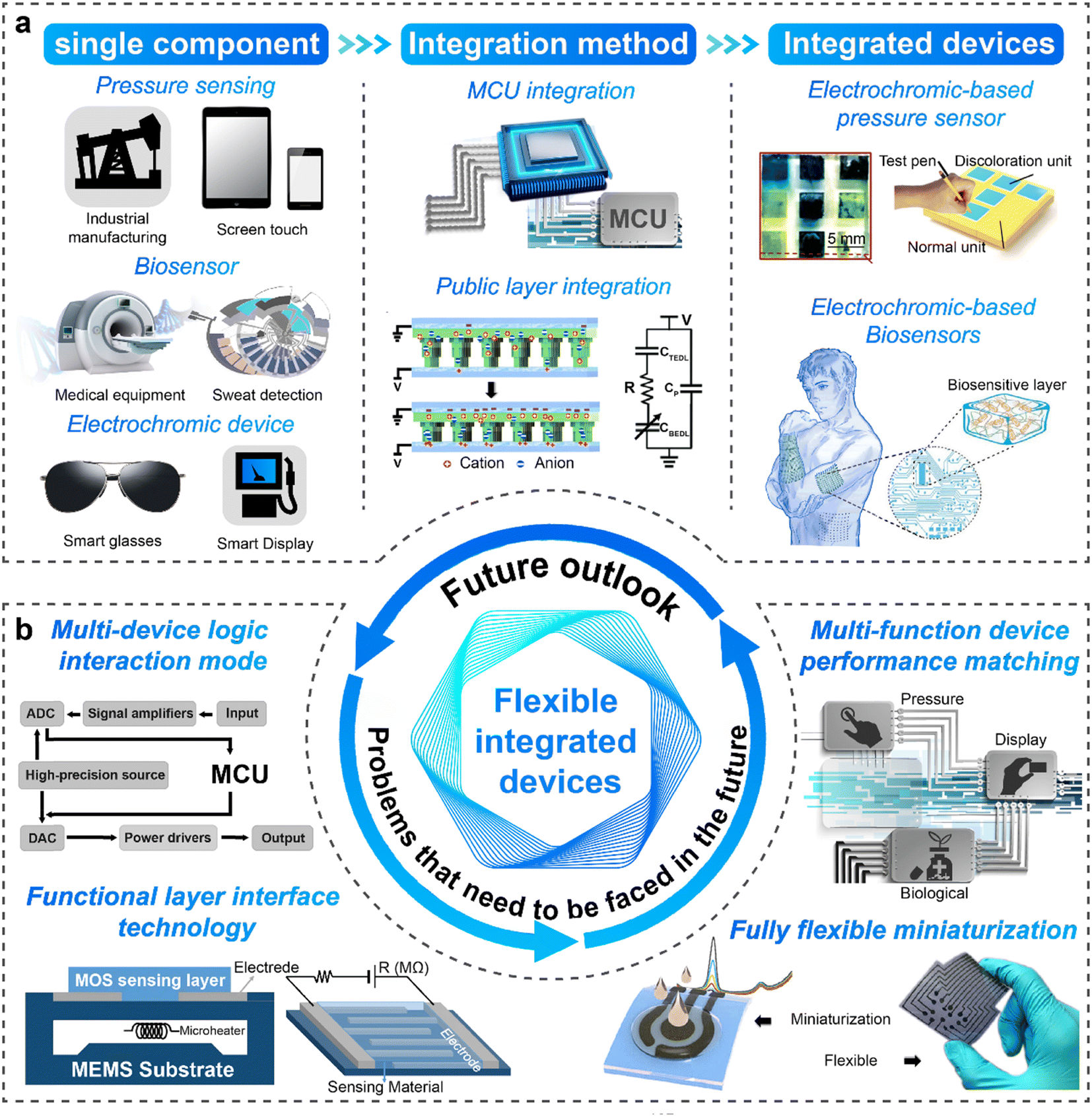 | ||
| Fig. 7 Problems faced by flexible integrated devices and future perspectives. (a) The integration roadmap of the biosensing platform. (b) The challenges in the future of the biosensing platform.16,191,198 Reproduced with permission from ref. 16, Copyright 2022, Wiley. Reproduced with permission from ref. 191, Copyright 2022, Elsevier. Reproduced with permission from ref. 198, Copyright 2022, Cell Press. Current issues to be addressed.58,63,199 Reproduced with permission from ref. 199, Copyright 2022, MDPI. Reproduced with permission from ref. 63, Copyright 2023, ACS. Reproduced with permission from ref. 58, Copyright 2023, Springer Nature. | ||
As an emerging field, EC-based visual biosensing devices are in the initial stage of vigorous development. Obviously, the integration of biosensing devices and ECDs faces several technical challenges in areas such as power constraints, interfacial mismatches, and signal coupling inefficiencies. Specifically, the first is a very serious problem: the link between the biosensing devices and the ECDs. Broadly speaking, the control logic of the biosensing devices and ECDs can be viewed as two interconnected closed-loop systems. The ECDs, along with the power supply and switch, are embedded within the sensor's loop. Each system performs a distinct function. The connection of the data collector to the switch enables the logical interaction between the biosensing/electrochemical displays and colour change. However, for the practical realisation of the interconnection, additional electronic components are needed, such as a comparator circuit and a microcontroller, leading to an increase in the system complexity. For example, visual pressure sensors can be fabricated by integrating stretchable ECDs and piezoresistive pressure sensors into summing amplifier circuits.15 A second challenge is faced when integrating functionally heterogeneous devices into a single multifunctional device through interface integration. Most publications on ECDs currently focus on synthesising novel or multifunctional materials or electrolytes while retaining the conventional framework structure. As a result, these strategies do not consider material interfaces and interface connections. Thus, a pressure-controlled EC multilayer device has been designed to mimic the natural response of skin from pressure to colouration.203 This pressure-sensitive colour-changing multifunctional design was vertically integrated into layered modules. The integrated device successfully realises the skin response without the peripheral circuits; thus, the flexible electronic device can directly display the pressure that was applied at each position. However, the pressure sensing module in the integrated device has a detection range of tens to hundreds of kPa. The normal human pulse, vocal cord vibration, joint bending, and other pressure values range from a few Pa to tens of Pa, and a larger grip force generally ranges from a few thousand Pa to a few hundred kPa, which far exceeds the actual pressure monitoring range of wearable devices. Therefore, further optimisation of this sensing device is still needed to monitor human physiological signals. Performance matching of the integrated devices is another problem to be solved. Motivated by the two-in-one response of an octopus, which can sense and visualise stimuli simultaneously, an integrated device for ion sensing and EC display with interactive pressure sensing has been proposed.16 This work directly embeds a bilayer capacitive pressure sensor into the conventional structure of an ECD, allowing for quantitative sensing and direct colour change in response to pressure via the efficient reuse of electrodes and ionic gels. However, the system still combines peripheral hybrid devices such as MCUs and Li-ion batteries. This complicates the device because it must perform the data acquisition, processing, and transmission processes.
In short, integrating sensor devices into simpler and smaller forms is another big challenge. In 2020, a lactic acid skin-patch-type self-powered EC tactile sensor was reported, which was prepared entirely by screen printing and could be easily read by the naked eye.204 An ionic gel consisting of polyvinylidene fluoride-co-hexafluoropropylene copolymer (PVDF-co-HFP), a gelling agent, and the ionic liquid 1-ethyl-3-methylimidazolium trifluoromethylsulfonate (EMIM-Tf) effectively separated the cathode (display) from the anode (tactile sensing). The device determined metabolites in sweat using 3 × 15 mm coloured strips as indicators, solving the challenge that most self-powered sensors cannot generate enough energy to drive a complete sensing system that includes sensors, displays, and data readout while effectively simplifying the integrated device. This autonomous skin-wearable monitoring display platform and power supply represent important progress in visual wearable electronics. Additionally, the analysis of key issues and synergistic strategies for integrated systems combining different biosensors with electrochromic devices is presented in Table 6.205
| Integrated system | Structure | Core advantage | Key challenge | Synergistic strategy |
|---|---|---|---|---|
| Pressure-ECDs | Distributed array-ECDs stack | Pressure-triggered contact area change → Electrical signal → Dual-mode EC tinting intensity output | Mechanical deformation mismatch | • Flexible material interpenetrating network |
| • Buckled micro-dome heterostructure | ||||
| • Pulsed EC drive | ||||
| Sweat-ECDs | Microchannel-embedded EC electrode | Shared sweat transport layer and EC layer electrodes reduce crosstalk | Electrochemical environment incompatibility | • Core–shell structure materials |
| • Sweat-electrolyte layer isolation cavities | ||||
| • Dual-frequency impedance spectrum decoupling | ||||
| Temperature-ECDs | Distributed quantum dot-Optical waveguide coupling | Temperature → Fluorescence peak shift → Waveguide transmission loss → EC light-intensity feedback control | Thermal drift interference | • Quantum dot-thermosensitive polymer hybrid film |
| • Distributed feedback laser (DFB) closed-loop control | ||||
| • Real-time thermodynamic model correction | ||||
| Humidity-ECDs | Porous EC photonic crystal | Humidity → Refractive index change → Photonic bandgap shift → Dual structural color/EC response | Swelling instability | • Material-confined water molecule channels |
| • Inverse opal EC resonator cavity | ||||
| • Atomic layer deposition encapsulation |
The integration process of ECDs with different types of biosensors is by no means a simple physical stacking but rather a complex systems engineering endeavor involving the deep fusion of materials, structures, performance, and working mechanisms.206 As for a pressure integration system, the core issue lies in the matching of mechanical interfaces. Specifically, in the pressure-ECD integrated system, a distributed array-ECD stacked structure is adopted, which converts pressure-triggered changes in the contact area into electrical signals, thereby driving the dual-mode coloring intensity output of ECDs. However, mechanical deformation mismatch between the pressure-sensing layer and the electronic display layer may lead to interfacial delamination or signal transmission distortion. To address this issue, a synergistic strategy focuses on constructing an interpenetrating network of flexible materials to enhance interfacial toughness. By leveraging the physical entanglement of polymer chains and dynamic reversible chemical bonds at the molecular scale, mechanical energy is efficiently dissipated, preventing interfacial delamination. A pyramid heterogeneous structure is designed to buffer stress and stabilize electrical contact at the micron scale. Additionally, a pulsed electronic actuator driving strategy is adopted to match the response time of dynamic pressure signals. The timing and intensity of voltage pulses are regulated based on the migration and diffusion kinetics of ions at the interface, ensuring synchronization between the electrochromic response and rapidly changing pressure signals.16
For the sweat-EC integrated system, a structure with microchannels embedded in EC electrodes is utilized to achieve shared sweat transport and display functions, aiming to reduce crosstalk.207 However, its core challenge stems from the incompatibility between the electrochemical environment of sensing and the working environment of ECDs. The competition for ion migration between sweat sensors and ECDs is fundamentally a chemical equilibrium issue arising from the conflict between limited interfacial ion flux and electrochemical potential gradients. Specifically, it manifests as electrochemical potential competition between biological ions (Na+/K+/H+) in sweat electrolytes and EC working ions (such as H+/Li+ in WO3 or K+ in Prussian blue) within shared transport channels, leading to mutual interference in ion flux. On one hand, the detection requirement for low-concentration biomarkers (e.g., lactate) in sweat conflicts with the high-concentration ion driving demand in the EC layer, resulting in an imbalance in concentration gradients and triggering overlapping migration path conflicts, which cause effective ion mobility to decay.208 On the other hand, free radicals (˙OH) generated by the oxidation of sweat sulfides (e.g., thiosulfate) attack the crystal lattice of EC materials, while the intercalation of EMIM+ cations into the WO3 lattice channels induces stress-accumulative cracks. Together, these effects lead to an electrode poisoning effect. Simultaneously, the concentration gradient imbalance between H+ in sweat and H+ in the EC layer weakens ion selectivity, causing Na+/Li+ to form a hybrid Helmholtz layer at the interface and generating parasitic capacitance interference. Corresponding solutions include developing composite materials with a core–shell structure to isolate sensitive active sites, designing a microfluidic structure with sweat-electrolyte layer isolation cavities to prevent cross-contamination, and employing dual-frequency impedance spectroscopy decoupling technology to distinguish and independently process sensing and driving signals.
In the temperature-EC integrated system, a distributed quantum dot-optical waveguide coupling mechanism is used to convert temperature changes into fluorescence peak shifts, which are then transmitted through waveguides to ultimately achieve EC light intensity feedback control.209 The core challenge of this approach is thermal drift interference with optical signals. To this end, collaborative strategies involve synthesizing a quantum dot-thermosensitive polymer hybrid film to enhance the thermo-optical coefficient, introducing a distributed feedback laser (DFB) for closed-loop control to improve measurement accuracy, and establishing a real-time thermodynamic model for online correction to compensate for errors caused by environmental fluctuations.
Moreover, the humidity-EC integrated system is based on a porous EC photonic crystal structure, which utilizes humidity-induced changes in refractive index to cause photonic bandgap shifts, thereby achieving dual structural color and EC responses. The main bottleneck of this system lies in the water-induced swelling instability of the sensitive material, which can disrupt the periodic structure of the photonic crystal and lead to signal drift.210 Innovative countermeasures include constructing functional materials with confined water molecule channels to control the direction and extent of swelling, fabricating an inverse opal-structured EC resonant cavity to maintain optical performance under expansion, and adopting atomic layer deposition (ALD) technology for nanoscale encapsulation to enhance the environmental stability and lifespan of the device. Therefore, the successful implementation of the heterogeneous integration of ECDs and biosensors relies on tailored collaborative design that accounts for the unique physicochemical properties of the specific integration target.
In the context of existing integrated schemes, it becomes evident that enhancing signal coupling efficiency is paramount in the integration of ECDs with flexible sensors. This efficiency dictates the efficacy with which electrical signals output by sensors drive ECDs to achieve optical responses. The core challenge of integrated devices lies in resolving energy conversion bottlenecks and signal fidelity issues, which directly impact the real-time performance and reliability of the system.211 However, the coupling efficiency of discrete components remains generally low, manifesting primarily in two aspects. Firstly, low power conversion efficiency (η_power) contributes to poor signal coupling.212 ECDs typically require a driving voltage of 1–3 V, while flexible sensors generally output signals below 1 V. This voltage incompatibility results in significant energy loss within conversion circuits. This is because the actual voltage driving the EC reaction must be higher than its thermodynamic equilibrium potential to provide this additional energy to overcome the reaction energy barrier. This difference is known as overpotential. A higher overpotential means less energy is used for driving the effective coloration reaction, and more electrical energy is wasted on initiating the reaction, thereby directly reducing the power conversion efficiency. Additionally, integrated devices are multilayer structured devices, and when charges transfer between interfaces of materials in different phases, they encounter resistance. These interfacial impedances lead to significant ohmic losses. A portion of the applied voltage is used to overcome these impedances rather than being entirely utilized to drive the effective redox reaction. Enhancing coupling efficiency significantly reduces power consumption. For instance, designing a self-powered ECD based on biofuel cells is feasible. The open-circuit voltage generated by biofuel cells can match the thermodynamic equilibrium potential of many electrochromic materials, enabling direct utilization of bioenergy for electrical conversion and significantly improving conversion efficiency. This challenge also resolves the issue by eliminating conversion circuits, and such direct coupling avoids additional energy losses caused by DC–DC boost conversion circuits. Secondly, response time delays impede real-time optoelectronic signal coupling. The response time difference (Δt) is defined as the delay between sensor activation and ECD coloration, which serves as a key quantitative metric. For example, WO3-based ECDs require several seconds to colorize, whereas pressure sensors respond within tens to hundreds of milliseconds. This asynchrony severely hinders real-time visualization of dynamic physiological signals. Optimizing ion and electron transport pathways through material synergy can mitigate this challenge.213 For instance, the development of core-shell nanostructures (e.g., WO3@PEDOT) significantly increases the effective reactive surface area, providing abundant reaction sites for ion intercalation/deintercalation. Moreover, in such core-shell nanostructures, both the core and shell are at the nanoscale, meaning the diffusion path for ions from the surface to the center of an individual core or shell particle is extremely short. As a result, the time required for diffusion (τ ≈ d2/D, where d is the diffusion distance and D is the diffusion coefficient) is substantially reduced. Additionally, from the perspective of external driving, dual-frequency impedance tuning can also reduce response delays. By employing a high-frequency signal to preemptively suppress the inefficient current consumption caused by parasitic capacitance, it thereby purifies the drive current and ensures that all energy is directed toward the effective electrochromic process.
The integration of ECDs and biosensing devices necessitates a holistic strategy centered on multimodal material design, synchronized structural engineering, thermodynamically optimized performance matching, and intelligent closed-loop systems (Fig. 8). Fig. 8a–d successively present the optimization routes of the intelligent platform, namely material innovation, structural design, performance matching and logical system integration. The core strategies and the existing challenges are presented. At the material level, this involves embedding sensing units (e.g., aptamers, enzymes) within electrochromic matrices (e.g. PEDOT networks, WO3 hybrids) to achieve dual functionality—though this fusion triggers quantum-scale conflicts such as d-orbital/HOMO-LUMO energy mismatches (>1 eV gap) and biomolecular entropy disruption under electric fields (>1 V μm−1). Structurally, architectures like vertical stacks, interdigital electrodes, and photonic crystals enable co-localized sensing-EC activation, yet suffer from optoelectronic crosstalk (e.g., ion diffusion noise >0.1 rad in optical paths) and fabrication disparities across nano-micro scales (e.g., <50 nm EC features vs. >100 μm microfluidics). Performance integration faces fundamental thermodynamic barriers: voltage incompatibilities (EC's 1–3 V vs. biosensors’ <1 V), electrolyte-induced bio-component degradation (>60% enzyme activity loss), and kinetic mismatches where EC coloration (100 ms–10 s) lags behind biological reactions (μs–ms). These culminate in systemic von Neumann bottlenecks, where analog-to-digital conversion (100 nJ per bit) and EC driving (1 μJ μm−2) impose unsustainable energy penalties, while nonlinear dynamics risk chaotic instability in feedback loops.214 Ultimately, achieving seamless EC-biosensing symbiosis demands transcending classical paradigms through quantum-enabled materials (topological insulators), entropy-harvesting systems, and neuromorphic computing to resolve energy-information conversion inefficiencies at their physical limits.
 | ||
| Fig. 8 The integration of ECDs and biosensing devices necessitates a holistic strategy centered on multimodal material design, synchronized structural engineering, thermodynamically optimized performance matching, and intelligent closed-loop systems. (a) Material innovation for integrated devices. (b) Structural design for integrated devices. (c) Performance matching of integrated devices. (d) The logical system design of integrated equipment. | ||
5. Conclusions
In summary, existing flexible tactile sensors are limited to a single electrical signal input/output, and the external stimuli are not directly visible to the human eye. The development of multiple tactile sensors integrated with ECDs overcomes this limitation, which is very significant for diversified applications in intelligent human–computer interactions. However, the development of multifunctional visual integrated devices depends heavily on the development and optimisation of single components. It is thus necessary to provide an optimisation route for the preparation of single components.With respect to flexible tactile sensors, it is of primary importance to develop novel sensitive materials that can respond to various stimuli. New materials lie at the heart of technological development. Recently, novel functional materials, including carbon materials, metal NWs and organic polymers, have led to great progress in the flexibility, stretchability, sensitivity, detection range, stability and multifunctionality of smart sensors. Material design also offers a powerful method for the development of material properties. Methods such as chemical doping and the surface modification of materials essentially change the composition of the material and adjust its electronic properties, endowing it with enhanced physicochemical properties. In addition, the continuous development of physical and chemical preparation techniques has enriched the microstructure of materials. Often, micro- and nano-functional materials with different microstructures, such as NWs, nanorods, nanodiscs, and a variety of bionanostructures, can be realised through simple and controllable preparation to meet the requirements of different application scenarios. Finally, the optimisation of device structures paves the way for portable, wearable and multifunctional integrated devices.
Electrochromic devices are developing groundbreaking composite architectures/strategies. First, new materials, including inorganic/organic materials, which have been flourishing, are overcoming the limits of ECDs in terms of flexibility and application range. Combining clever molecular design, structural colour and material composites provides an effective way to realise colour modulation and performance optimisation of ECDs. Moreover, device design strategies, including colouring of electrodes, complementary colouring of electrodes, colouring of the electrolyte, and colouring of the substrate of electrodes, provide an effective way to simplify the complex structure of the device and enhance integrated devices.
However, multi-functional integrated devices still have a number of issues that need to be solved beyond the single-component optimisation strategy. The first involves signal conversion and compatibility between the tactile sensor and the electrochromic (EC) display element. The second involves logical interaction between the contact sensor and the EC display element without relying on a peripheral circuit. From these, the first requirement for visual integration of the device is that the flexible tactile sensor should be able to set the sensitivity at different resistive mode values and switch range thresholds to drive the real-time colour change response of the EC display element. The main operational constraint for ECDs is that touch sensors should yield a large resistance range so that the system can be activated directly without external circuitry. Typically, ECDs need a drive voltage of approximately 1 V and a peak current of approximately 30 mA in order to respond in time; that is, the resistance of the tactile sensor should be exceedingly low in the ‘on’ state and high enough in the 'off' state. The second requirement is the ability for the controller to be in direct series connection with the switch, which is crucial to providing a logical interaction between the sensing of the biosignal and the response of the colour-changing display. By building piezoresistive, piezoelectric tactile sensors, biological signals can be perceived and converted into voltage signals, allowing the display element to be directly turned on and off in series through the common electrode. This is one effective way to achieve visual integrated devices without peripheral circuits. Researchers have already developed several different visualisation sensors. However, the combination of EC-based visual flexible tactile sensing platforms still faces many difficulties, such as logic interaction circuits, output performance matching, interface connection technology, full flexibility and miniaturisation. These aspects offer many opportunities for impactful research.
Future EC-based visual flexible biosensing platforms need to achieve breakthroughs in the following aspects. Firstly, synergistic innovation in materials and interfaces. The core breakthrough of future platforms will rely on multimodal material design. For instance, by developing smart materials such as quantum dot-thermoresponsive polymer hybrid films, the functional integration of biosignal response and optical feedback can be simultaneously achieved. However, material interfaces still face challenges such as energy-level mismatch between biological and non-biological systems and biomolecule deactivation caused by electrolyte penetration. Solutions include constructing core-shell structures to isolate sensitive sites, such as WO3@PEDOT core-shell nanomaterials, while utilizing atomic layer deposition (ALD) technology to achieve nanoscale encapsulation and enhance stability. Secondly, optimization of structure and energy efficiency. Device structures will evolve toward bio-integrated directions, such as photonic crystal resonators enabling humidity-optical dual responses, but challenges like optical path drift caused by water-induced swelling must be overcome. The breakthrough lies in constructing inverse opal-structured EC resonators combined with microchannel isolation designs to suppress signal crosstalk. In terms of energy efficiency, the compatibility between EC driving voltage and biosensor signals needs to be addressed. This can be achieved by drawing inspiration from self-powered ECDs that use biofuel cells to directly convert biological energy into optical signals, thereby improving power conversion efficiency, while employing dual-frequency impedance spectroscopy decoupling technology to eliminate parasitic capacitance interference. Thirdly, reconfiguration of intelligent closed-loop systems. The leap from discrete components to autonomous perception-decision systems requires overcoming the von Neumann bottleneck. Current systems struggle to support real-time multi-parameter feedback due to energy consumption limitations in analog-to-digital conversion and EC driving. Future developments will focus on pulse neural network architectures, utilizing distributed feedback lasers (DFB) to achieve closed-loop control of optical signals, combined with thermodynamic models for online correction of environmental drift. For example, quantum dot-optical waveguide coupling systems can map temperature changes through fluorescence peak shifts but require real-time compensation algorithms to suppress measurement errors. Fourthly, biocompatibility is necessary. The goal is to construct a life-like perception-response cycle. Urgent challenges include achieving mechanical/electrochemical matching between flexible interfaces and tissues, such as reducing the device's Young's modulus to <100 kPa to achieve dermal-level conformal attachment. Implementation strategies may involve enhancing interface toughness through biomimetic microporous topological structures and improving biocompatibility with skin-adhesive hydrogels.
Electrically conductive biosensing platforms are evolving from single-function devices to integrated perception-feedback-decision systems. Their development will depend on synergistic breakthroughs in material genetic engineering, heterogeneous integration strategies, and entropy-controlled intelligent systems, ultimately driving wearable devices and human-computer interaction technologies from passive monitoring to active intervention.
Author contributions
C. P., Z. Y., and Y. L. proposed and supervised the project; Y. Z., J. Q., R. B., and Y. L. wrote the review together.Conflicts of interest
There are no conflicts to declare.Data availability
No primary research results, software or code have been included and no new data were generated or analysed as part of this review.Acknowledgements
The authors appreciate support from the National Natural Science Foundation of China (No. 62404087, 52192610, 62422120, 52371202, 52125205, 52250398 and 52472002), the Natural Science Foundation of Yunnan Province (202401AU070161), the Science and Technology Project of the Southwest Joint Graduate School of Yunnan Province (202302A0370008), the Key Project of the National Natural Science Foundation of China-Yunnan Joint Fund (U2102215), the Academician Expert Workstation of Cherkasova Tatiana in Yunnan Province (202305AF150099), the Yunnan Province Major Science and Technology Special Plan (202302AB080005), the Preparation and Property Control of Luminescent Materials and Application in Plateau Agriculture (yfgrc202407), the Natural Science Foundation of the Beijing Municipality (L223006), the Shenzhen Science and Technology Program (Grant No. KQTD20170810105439418), and the Fundamental Research Funds for the Central Universities.References
- Y. Lu, X. Qu, W. Zhao, Y. Ren, W. Si, W. Wang, Q. Wang, W. Huang and X. Dong, Research, 2020, 2038560 CAS.
- X. Bai, Y. Cun, Z. Xu, Y. Zi, A. A. Haider, A. Ullah, I. Khan, J. Qiu, Z. Song and Z. Yang, Chem. Eng. J., 2022, 429, 132333 CrossRef CAS.
- J. He, R. Wei, S. Ge, W. Wu, J. Guo, J. Tao, R. Wang, C. Wang and C. Pan, InfoMat, 2024, 6, e12493 CrossRef.
- Z. P. He, B. N. Sun, H. Lu, X. D. Sun, Z. S. Xu, Y. G. Liang, Q. C. Lu, Y. Yu, K. Y. Hu, S. Poddar, W. Q. Wu, W. C. Gao, X. Han, Z. Y. Fan and C. F. Pan, Sci. Adv., 2025, 11, eadw7826 CrossRef PubMed.
- Y. Zhang, C. Wang, J. Tao, S. Ma, S. Xie, W. Guo, R. Bao, J. Qiu, Y. Liu, Z. Yang and C. Pan, Adv. Sci., 2025, e15117 CrossRef PubMed.
- R. Yang, A. Dutta, B. Li, N. Tiwari, W. Zhang, Z. Niu, Y. Gao, D. Erdely, X. Xin, T. Li and H. Cheng, Nat. Commun., 2023, 14, 2907 CrossRef CAS PubMed.
- L. B. Baker, J. B. Model, K. A. Barnes, M. L. Anderson, S. P. Lee, K. A. Lee, S. D. Brown, A. J. Reimel, T. J. Roberts, R. P. Nuccio, J. L. Bonsignore, C. T. Ungaro, J. M. Carter, W. Li, M. S. Seib, J. T. Reeder, A. J. Aranyosi, J. A. Rogers and R. Ghaffari, Sci. Adv., 2020, 6, eabe3929 CrossRef CAS PubMed.
- Q. Hua, J. Sun, H. Liu, R. Bao, R. Yu, J. Zhai, C. Pan and Z. L. Wang, Nat. Commun., 2018, 9, 244 CrossRef PubMed.
- S. Hao, Q. Fu, L. Meng, F. Xu and J. Yang, Nat. Commun., 2022, 13, 6472 CrossRef CAS PubMed.
- S. Li, Y. Zhang, X. Liang, H. Wang, H. Lu, M. Zhu, H. Wang, M. Zhang, X. Qiu, Y. Song and Y. Zhang, Nat. Commun., 2022, 13, 5416 CrossRef CAS PubMed.
- B. Wang, Y. Huang, Y. Han, S. Zhao, W. Ding, W. Zhang, R. Li, X. Wu, Q. Jiang, Y. Li, D. Gao, Y. Zhao, F. Wang, H. Jiang and R. Zhang, Cell Rep. Phys. Sci., 2023, 4, 101408 CrossRef CAS.
- Y. Li, P. Sun, J. Chen, X. Zha, X. Tang, Z. Chen, Y. Zhang, S. Cong, F. Geng and Z. Zhao, Adv. Mater., 2023, 35, e2300116 CrossRef PubMed.
- J. Koo, V. Amoli, S. Y. Kim, C. Lee, J. Kim, S.-M. Park, J. Kim, J. M. Ahn, K. J. Jung and D. H. Kim, Nano Energy, 2020, 78, 105199 CrossRef CAS.
- C. Gu, S. Wang, J. He, Y.-M. Zhang and S. X.-A. Zhang, Chem., 2023, 9, 2841 CAS.
- H. H. Chou, A. Nguyen, A. Chortos, J. W. To, C. Lu, J. Mei, T. Kurosawa, W. G. Bae, J. B. Tok and Z. Bao, Nat. Commun., 2015, 6, 8011 CrossRef CAS PubMed.
- Y. Guo, H. Li, Y. Li, X. Wei, S. Gao, W. Yue, C. Zhang, F. Yin, S. Zhao, N. Y. Kim and G. Shen, Adv. Funct. Mater., 2022, 32, 2203585 CrossRef CAS.
- G. Wu, X. Li, R. Bao and C. Pan, Adv. Funct. Mater., 2024, 34, 2405722 CrossRef CAS.
- F. Basarir, Z. Madani and J. Vapaavuori, Adv. Mater. Interfaces, 2022, 9, 2200866 CrossRef CAS.
- D. Lei, N. Liu, T. Su, Q. Zhang, L. Wang, Z. Ren and Y. Gao, Adv. Mater., 2022, 34, e2110608 CrossRef PubMed.
- N. Luo, Y. Huang, J. Liu, S. C. Chen, C. P. Wong and N. Zhao, Adv. Mater., 2017, 29, 1702675 CrossRef PubMed.
- X. Li, J. Wang, Y. Lin, Y. Cheng, W. Han, G. Yuan and H. Jia, Colloids Surf., A, 2022, 635, 128091 CrossRef CAS.
- F. Basarir, J. J. Kaschuk and J. Vapaavuori, Biosensors, 2022, 12, 12040187 CrossRef PubMed.
- Z. Gao, X. Xiao, A. D. Carlo, J. Yin, Y. Wang, L. Huang, J. Tang and J. Chen, Adv. Funct. Mater., 2023, 33, 2214265 CrossRef CAS.
- J. Baek, Y. Shan, M. Mylvaganan, Y. Zhang, X. Yang, F. Qin, K. Zhao, H. W. Song, H. Mao and S. Lee, Adv. Mater., 2023, 35, e2304070 CrossRef PubMed.
- J. O. Kim, S. Y. Kwon, Y. Kim, H. B. Choi, J. C. Yang, J. Oh, H. S. Lee, J. Y. Sim, S. Ryu and S. Park, ACS Appl. Mater. Interfaces, 2019, 11, 1503 CrossRef CAS PubMed.
- Y. Liu, J. Tao, Y. Mo, R. Bao and C. Pan, Adv. Mater., 2024, 36, e2313857 CrossRef PubMed.
- R. B. Mishra, N. El-Atab, A. M. Hussain and M. M. Hussain, Adv. Mater. Technol., 2021, 6, 2001023 CrossRef.
- W. Lin, B. Wang, G. Peng, Y. Shan, H. Hu and Z. Yang, Adv. Sci., 2021, 8, 2002817 CrossRef CAS PubMed.
- Z. Wang, Z. Liu, G. Zhao, Z. Zhang, X. Zhao, X. Wan, Y. Zhang, Z. L. Wang and L. Li, ACS Nano, 2022, 16, 1661 CrossRef CAS PubMed.
- J. Hu, G. Dun, X. Geng, J. Chen, X. Wu and T. L. Ren, Nanoscale Adv., 2023, 5, 3131 RSC.
- Y. Zhang, J. Yang, X. Hou, G. Li, L. Wang, N. Bai, M. Cai, L. Zhao, Y. Wang, J. Zhang, K. Chen, X. Wu, C. Yang, Y. Dai, Z. Zhang and C. F. Guo, Nat. Commun., 2022, 13, 1317 CrossRef CAS PubMed.
- X. Qu, J. Li, Z. Han, Q. Liang, Z. Zhou, R. Xie, H. Wang and S. Chen, ACS Nano, 2023, 17, 14904 CrossRef CAS PubMed.
- M. Jing, J. Zhou, P. Zhang, D. Hou, J. Shen, J. Tian and W. Chen, ACS Appl. Mater. Interfaces, 2022, 14, 55119 CrossRef CAS PubMed.
- R. Liu, Y. Liu, Y. Cheng, H. Liu, S. Fu, K. Jin, D. Li, Z. Fu, Y. Han, Y. Wang and Y. Tian, Adv. Funct. Mater., 2023, 33, 2308175 CrossRef CAS.
- W. Zhu, J. Wang, W. Sun, S. Zhou and M. He, Chem. Eng. J., 2023, 451, 138335 CrossRef CAS.
- P. Zhang, J. Zhang, Y. Li and L. Huang, J. Phys. D: Appl. Phys., 2021, 54, 465401 CrossRef CAS.
- Q. Liu, Z. Liu, C. Li, K. Xie, P. Zhu, B. Shao, J. Zhang, J. Yang, J. Zhang, Q. Wang and C. F. Guo, Adv. Sci., 2020, 7, 2000348 CrossRef CAS PubMed.
- L. Shi, Z. Li, M. Chen, Y. Qin, Y. Jiang and L. Wu, Nat. Commun., 2020, 11, 3529 CrossRef CAS PubMed.
- J. C. Yang, J. O. Kim, J. Oh, S. Y. Kwon, J. Y. Sim, D. W. Kim, H. B. Choi and S. Park, ACS Appl. Mater. Interfaces, 2019, 11, 19472 CrossRef CAS PubMed.
- N. Bai, L. Wang, Q. Wang, J. Deng, Y. Wang, P. Lu, J. Huang, G. Li, Y. Zhang, J. Yang, K. Xie, X. Zhao and C. F. Guo, Nat. Commun., 2020, 11, 209 CrossRef CAS PubMed.
- L. Cai, G. Chen, J. Tian, B. Su and M. He, Chem. Mater., 2021, 33, 2072 CrossRef CAS.
- T. Yang, W. Deng, X. Chu, X. Wang, Y. Hu, X. Fan, J. Song, Y. Gao, B. Zhang, G. Tian, D. Xiong, S. Zhong, L. Tang, Y. Hu and W. Yang, ACS Nano, 2021, 15, 11555 CrossRef CAS PubMed.
- N. Bai, L. Wang, Y. Xue, Y. Wang, X. Hou, G. Li, Y. Zhang, M. Cai, L. Zhao, F. Guan, X. Wei and C. F. Guo, ACS Nano, 2022, 16, 4338 CrossRef CAS PubMed.
- Y. Xiong, Y. Shen, L. Tian, Y. Hu, P. Zhu, R. Sun and C.-P. Wong, Nano Energy, 2020, 70, 104436 CrossRef CAS.
- J. Xu, L. Zhang, X. Lai, X. Zeng and H. Li, ACS Appl. Mater. Interfaces, 2022, 14, 27262 CrossRef CAS PubMed.
- Y. He, Y. Huang, R. Xue, Q. Shi, Y. Wu and R. Liu, Diamond Relat. Mater., 2023, 140, 110536 CrossRef CAS.
- X. Zheng, S. Zhang, M. Zhou, H. Lu, S. Guo, Y. Zhang, C. Li and S. C. Tan, Adv. Funct. Mater., 2023, 33, 2214880 CrossRef CAS.
- R. L. Truby and J. A. Lewis, Nature, 2016, 540, 371–378 CrossRef CAS PubMed.
- S. Li, K. Li, C. Yi, X. Gao and Z. Gan, Nat. Commun., 2025, 16, 6449 CrossRef CAS PubMed.
- N. C. Brown, D. C. Ames and J. Mueller, Nat. Rev. Mater., 2025, 1–19 Search PubMed.
- J. Li, J. Cao, B. Lu and G. Gu, Nat. Rev. Mater., 2023, 8, 604–622 CrossRef.
- J. Jiang, C. Yuan, X. Zhang, L. Gu, Y. Yao, X. Wang, Y. He and L. Shao, Adv. Mater., 2024, 36, e2412127 CrossRef PubMed.
- Y. Jin, S. Xue and Y. He, Adv. Mater., 2025, 37, e2500076 CrossRef PubMed.
- S. Wang, W. Deng, T. Yang, Y. Ao, H. Zhang, G. Tian, L. Deng, H. Huang, J. Huang, B. Lan and W. Yang, Adv. Funct. Mater., 2023, 33, 2214503 CrossRef CAS.
- W. Cheng, X. Wang, Z. Xiong, J. Liu, Z. Liu, Y. Jin, H. Yao, T. S. Wong, J. S. Ho and B. C. K. Tee, Nat. Mater., 2023, 22, 1352 CrossRef CAS PubMed.
- L. Shi, Z. Li, M. Chen, T. Zhu and L. Wu, Adv. Mater., 2023, 35, e2210091 CrossRef PubMed.
- Q. Su, Q. Zou, Y. Li, Y. Chen, S.-Y. Teng, J. T. Kelleher, R. Nith, P. Cheng, N. Li, W. Liu, S. Dai, Y. Liu, A. Mazursky, J. Xu, L. Jin, P. Lopes and S. Wang, Sci. Adv., 2021, 7, eabi4563 CrossRef PubMed.
- F. Gao, C. Liu, L. Zhang, T. Liu, Z. Wang, Z. Song, H. Cai, Z. Fang, J. Chen, J. Wang, M. Han, J. Wang, K. Lin, R. Wang, M. Li, Q. Mei, X. Ma, S. Liang, G. Gou and N. Xue, Microsyst. Nanoeng., 2023, 9, 1 CrossRef PubMed.
- Y. Du, X. Zhang, P. Liu, D. G. Yu and R. Ge, Front. Chem., 2022, 10, 944428 CrossRef CAS PubMed.
- M. Liu, S. Wang, Z. Xiong, Z. Zheng, N. Ma, L. Li, Q. Gao, C. Ge, Y. Wang and T. Zhang, Biosens. Bioelectron., 2023, 237, 115504 CrossRef CAS PubMed.
- C.-H. Wu, H. J. H. Ma, P. Baessler, R. K. Balanay and T. R. Ray, Sci. Adv., 2023, 9, eadg4272 CrossRef CAS PubMed.
- I. Shitanda, Y. Ozone, Y. Morishita, H. Matsui, N. Loew, M. Motosuke, T. Mukaimoto, M. Kobayashi, T. Mitsuhara, Y. Sugita, K. Matsuo, S. Yanagita, T. Suzuki, T. Mikawa, H. Watanabe and M. Itagaki, ACS Sens., 2023, 8, 2368 CrossRef CAS PubMed.
- L. Yang, H. Wang, A. M. Abdullah, C. Meng, X. Chen, A. Feng and H. Cheng, ACS Appl. Mater. Interfaces, 2023, 15, 34332 CrossRef CAS PubMed.
- Y. Qin, J. Mo, Y. Liu, S. Zhang, J. Wang, Q. Fu, S. Wang and S. Nie, Adv. Funct. Mater., 2022, 32, 2201846 CrossRef CAS.
- H. Li, T. Chang, Y. Gai, K. Liang, Y. Jiao, D. Li, X. Jiang, Y. Wang, X. Huang, H. Wu, Y. Liu, J. Li, Y. Bai, K. Geng, N. Zhang, H. Meng, D. Huang, Z. Li, X. Yu and L. Chang, Nano Energy, 2022, 92, 106786 CrossRef CAS.
- L. Wang, J. Lu, Q. Li, L. Li, E. He, Y. Jiao, T. Ye and Y. Zhang, Adv. Funct. Mater., 2022, 32, 2200922 CrossRef CAS.
- J. He, R. Wei, X. Ma, W. Wu, X. Pan, J. Sun, J. Tang, Z. Xu, C. Wang and C. Pan, Adv. Mater., 2024, 36, 2401931 CrossRef CAS PubMed.
- S. Kim, S. Park, J. Choi, W. Hwang, S. Kim, I. S. Choi, H. Yi and R. Kwak, Nat. Commun., 2022, 13, 6705 CrossRef CAS PubMed.
- X. He, C. Fan, Y. Luo, T. Xu and X. Zhang, npj Flexible Electron., 2022, 6, 60 CrossRef CAS.
- S. Honda, R. Tanaka, G. Matsumura, N. Seimiya and K. Takei, Adv. Funct. Mater., 2023, 33, 2306516 CrossRef CAS.
- X. Xuan, H. S. Yoon and J. Y. Park, Biosens. Bioelectron., 2018, 109, 75 CrossRef CAS PubMed.
- A. B. Radwan, S. Paramparambath, J. J. Cabibihan, A. K. Al-Ali, P. Kasak, R. A. Shakoor, R. A. Malik, S. A. Mansour and K. K. Sadasivuni, Biosensors, 2021, 11, 463 CrossRef CAS PubMed.
- Y.-X. Wang, P.-K. Tsao, M. Rinawati, K.-J. Chen, K.-Y. Chen, C. Y. Chang and M.-H. Yeh, Chem. Eng. J., 2022, 427, 131687 CrossRef CAS.
- P. Li, Z. Ling, X. Liu, L. Bai, W. Wang, H. Chen, H. Yang, L. Yang and D. Wei, Chem. Eng. J., 2023, 466, 143306 CrossRef CAS.
- V. Mazzaracchio, A. Serani, L. Fiore, D. Moscone and F. Arduini, Electrochim. Acta, 2021, 394, 139050 CrossRef CAS.
- X. Hou, Y. Zhou, Y. Liu, L. Wang and J. Wang, J. Mater. Sci., 2020, 55, 16033 CrossRef CAS.
- W. He, C. Wang, H. Wang, M. Jian, W. Lu, X. Liang, X. Zhang, F. Yang and Y. Zhang, Sci. Adv., 2019, 5, eaax0649 CrossRef CAS PubMed.
- J. Tu, J. Min, Y. Song, C. Xu, J. Li, J. Moore, J. Hanson, E. Hu, T. Parimon, T. Y. Wang, E. Davoodi, T. F. Chou, P. Chen, J. J. Hsu, H. B. Rossiter and W. Gao, Nat. Biomed. Eng., 2023, 7, 1293 CrossRef CAS PubMed.
- Y. Yang, Y. Song, X. Bo, J. Min, O. S. Pak, L. Zhu, M. Wang, J. Tu, A. Kogan, H. Zhang, T. K. Hsiai, Z. Li and W. Gao, Nat. Biotechnol., 2020, 38, 217 CrossRef CAS PubMed.
- Y. Song, J. Min, Y. Yu, H. Wang, Y. Yang, H. Zhang and W. Gao, Sci. Adv., 2020, 6, eaay9842 CrossRef CAS PubMed.
- Y. Dong, T. L. Liu, S. Chen, P. Nithianandam, K. Matar and J. Li, Adv. Funct. Mater., 2023, 33, 2210136 CrossRef CAS PubMed.
- H. Y. Y. Nyein, L.-C. Tai, Q. P. Ngo, M. Chao, G. B. Zhang, W. Gao, M. Bariya, J. Bullock, H. Kim, H. M. Fahad and A. Javey, ACS Sens., 2018, 3, 944 CrossRef CAS PubMed.
- G. Ibanez-Redin, G. Rosso Cagnani, O. G. N. P. A. Raymundo-Pereira, S. M. S. A. M. A. Gutierrez, J. E. Krieger and O. N. Oliveira Jr., Biosens. Bioelectron, 2023, 223, 114994 CrossRef CAS PubMed.
- T. Yan, G. Zhang, K. Yu, H. Chai, M. Tian, L. Qu, H. Dong and X. Zhang, Chem. Eng. J., 2023, 455, 140779 CrossRef CAS.
- J. Xiao, C. Fan, T. Xu, L. Su and X. Zhang, Sens. Actuators, B, 2022, 359, 131586 CrossRef CAS.
- S. Y. Oh, S. Y. Hong, Y. R. Jeong, J. Yun, H. Park, S. W. Jin, G. Lee, J. H. Oh, H. Lee, S. S. Lee and J. S. Ha, ACS Appl. Mater. Interfaces, 2018, 10, 13729 CrossRef CAS PubMed.
- Y. Wang, H. Guo, M. Yuan, J. Yu, Z. Wang and X. Chen, Talanta, 2023, 257, 124362 CrossRef CAS PubMed.
- R. Eslami, N. Azizi, S. R. Ghaffarian, M. Mehrvar and H. Zarrin, Electrochim. Acta, 2022, 404, 139749 CrossRef CAS.
- M. Li, L. Wang, R. Liu, J. Li, Q. Zhang, G. Shi, Y. Li, C. Hou and H. Wang, Biosens. Bioelectron., 2021, 174, 112828 CrossRef CAS PubMed.
- X. Huang, J. Li, Y. Liu, T. Wong, J. Su, K. Yao, J. Zhou, Y. Huang, H. Li, D. Li, M. Wu, E. Song, S. Han and X. Yu, Bio-Des. Manuf., 2021, 5, 201 CrossRef.
- G. Ge, Y. Lu, X. Qu, W. Zhao, Y. Ren, W. Wang, Q. Wang, W. Huang and X. Dong, ACS Nano, 2020, 14, 218 CrossRef CAS PubMed.
- S. Kim, S. Lim, M. H. Jeong, W. Kim, S. Baik and J. W. Suk, J. Mater. Sci. Technol., 2024, 172, 15 CrossRef CAS.
- J. Huang, X. Liu and Y. Du, J. Mater., 2024, 10, 173 Search PubMed.
- T. Yang, D. Yu, D. Wang, T. Yang, Z. Li, M. Wu, M. Petru and J. Crittenden, Appl. Catal., B, 2021, 286, 119859 CrossRef CAS.
- B. Han, H. Wang, W. Yang, J. Wang and X. Wei, Ceram. Int., 2021, 47, 9477 CrossRef CAS.
- X. Zhang, Y. Wang, X. Gao, Y. Ji, F. Qian, J. Fan, H. Wang, L. Qiu, W. Li and H. Yang, ACS Appl. Mater. Interfaces, 2021, 13, 47764 CrossRef CAS PubMed.
- D. Lv, W. Chen, W. Shen, M. Peng, X. Zhang, R. Wang, L. Xu, W. Xu, W. Song and R. Tan, Sens. Actuators, B, 2019, 298, 126890 CrossRef CAS.
- J. Zhou, S. Jin, C. Chai, M. Hao, X. Zhong, T. Ying, J. Guo and X. Chen, Innovation, 2022, 3, 100204 CAS.
- H. Liu, K. Sun, X. L. Guo, Z. L. Liu, Y. H. Wang, Y. Yang, D. Yu, Y. T. Li and T. L. Ren, ACS Nano, 2022, 16, 21527 CrossRef CAS PubMed.
- J. Qin, L. J. Yin, Y. N. Hao, S. L. Zhong, D. L. Zhang, K. Bi, Y. X. Zhang, Y. Zhao and Z. M. Dang, Adv. Mater., 2021, 33, e2008267 CrossRef PubMed.
- C. Okutani, T. Yokota and T. Someya, Adv. Sci., 2022, 9, e2202312 CrossRef PubMed.
- A. J. Cheng, L. Wu, Z. Sha, W. Chang, D. Chu, C. H. Wang and S. Peng, Adv. Mater. Technol., 2023, 8, 2201959 CrossRef.
- Z. Liu, B. Tian, Z. Jiang, S. Li, J. Lei, Z. Zhang, J. Liu, P. Shi and Q. Lin, Int. J. Extreme Manuf., 2022, 5, 015601 CrossRef.
- Q. Zhang, K. Zhang, D. Xu, G. Yang, H. Huang, F. Nie, C. Liu and S. Yang, Progress in Mater. Sci., 2014, 60, 208 CrossRef CAS.
- G. Zhang, P. Li, X. Wang, Y. Xia and J. Yang, Adv. Funct. Mater., 2023, 33, 2208900 CrossRef CAS.
- S. Cho, H. Han, H. Park, S.-U. Lee, J.-H. Kim, S. W. Jeon, M. Wang, R. Avila, Z. Xi, K. Ko, M. Park, J. Lee, M. Choi, J.-S. Lee, W. G. Min, B.-J. Lee, S. Lee, J. Choi, J. Gu, J. Park, M. S. Kim, J. Ahn, O. Gul, C. Han, G. Lee, S. Kim, K. Kim, J. Kim, C.-M. Kang, J. Koo, S. S. Kwak, S. Kim, D. Y. Choi, S. Jeon, H. J. Sung, Y. B. Park, M. Je, Y. T. Cho, Y. S. Oh and I. Park, npj Flexible Electron., 2023, 7(8) Search PubMed.
- N. T. Tien, Y. G. Seol, L. H. A. Dao, H. Y. Noh and N. E. Lee, Adv. Mater., 2009, 21, 910 CrossRef.
- X. F. Zhao, S. Q. Yang, X. H. Wen, Q. W. Huang, P. F. Qiu, T. R. Wei, H. Zhang, J. C. Wang, D. W. Zhang, X. Shi and H. L. Lu, Adv. Mater., 2022, 34, e2107479 CrossRef PubMed.
- S. Hao, L. Meng, Q. Fu, F. Xu and J. Yang, Chem. Eng. J., 2022, 431, 133782 CrossRef CAS.
- H. Liu, C. Du, L. Liao, H. Zhang, H. Zhou, W. Zhou, T. Ren, Z. Sun, Y. Lu, Z. Nie, F. Xu, J. Zhu and W. Huang, Nat. Commun., 2022, 13, 3420 CrossRef CAS PubMed.
- L. Chen, X. Chang, H. Wang, J. Chen and Y. Zhu, Nano Energy, 2022, 96, 107077 CrossRef CAS.
- Y. Lu, H. Zhang, Y. Zhao, H. Liu, Z. Nie, F. Xu, J. Zhu and W. Huang, Adv. Mater., 2024, 36, e2310613 CrossRef PubMed.
- J. Song, Y. Wei, M. Xu, J. Gao, L. Luo, H. Wu, X. Li, Y. Li and X. Wang, ACS Appl. Polym. Mater., 2022, 4, 766 CrossRef CAS.
- Y. Song, S. Wang, B. Gao, A. Chang and W. Kong, Adv. Mater. Interfaces, 2023, 10, 2202274 CrossRef CAS.
- N. Wang, H. Sun, X. Yang, W. Lin, W. He, H. Liu, G. Bhat and B. Yu, Sens. Actuators, A, 2022, 339, 113519 CrossRef CAS.
- W. M. Ryu, Y. Lee, Y. Son, G. Park and S. Park, Adv. Fiber Mater., 2023, 5, 1712 CrossRef CAS.
- X. Chen, R. Li, G. Niu, M. Xin, G. Xu, H. Cheng and L. Yang, Chem. Eng. J., 2022, 444, 136631 CrossRef CAS.
- Q. Wang, J. Zeng, J. Li, S. Yu, M. T. Innocent, M. Li, W. Ma, H. Xiang and M. Zhu, Adv. Compos. Hybrid Mater., 2022, 6, 26 CrossRef.
- E. Song, M. Chen, Z. Chen, Y. Zhou, W. Zhou, H. T. Sun, X. Yang, J. Gan, S. Ye and Q. Zhang, Nat. Commun., 2022, 13, 2166 CrossRef CAS PubMed.
- M. Lin, Z. Zheng, L. Yang, M. Luo, L. Fu, B. Lin and C. Xu, Adv. Mater., 2022, 34, e2107309 CrossRef PubMed.
- J. Wu, Z. Wu, Y. Wei, H. Ding, W. Huang, X. Gui, W. Shi, Y. Shen, K. Tao and X. Xie, ACS Appl. Mater. Interfaces, 2020, 12, 19069 CrossRef CAS PubMed.
- S. Yamada and H. Toshiyoshi, ACS Appl. Mater. Interfaces, 2020, 12, 36449 CrossRef CAS PubMed.
- H. Wang, Y. Mao, D. Ji, L. Wang, L. Wang, J. Chen, X. Chang and Y. Zhu, Chem. Eng. J., 2023, 471, 144674 CrossRef CAS.
- P. Yao, Q. Bao, Y. Yao, M. Xiao, Z. Xu, J. Yang and W. Liu, Adv. Mater., 2023, 35, e2300114 CrossRef PubMed.
- Z. Han, L. Mo, S. Han, Z. Sun, W. Ma, H. Hu, M. Geng, L. Liu, Z. Xin, K. Hu, H. Li and X. Chen, Small, 2025, 21, e2407168 CrossRef PubMed.
- Y. Zhang, Z. Ming, Z. Zhou, X. Wei, J. Huang, Y. Zhang, W. Li, L. Zhu, S. Wang, M. Wu, Z. Lu, X. Zhou and J. Xiong, Nat. Commun., 2025, 16, 6785 CrossRef CAS PubMed.
- X. L. Shi, N. H. Li, M. Li and Z. G. Chen, Chem. Rev., 2025, 125, 7525–7724 CrossRef CAS PubMed.
- L. Liu, Y. Dou, J. Wang, Y. Zhao, W. Kong, C. Ma, D. He, H. Wang, H. Zhang, A. Chang and P. Zhao, Adv. Sci., 2024, 11, e2405003 CrossRef PubMed.
- G. Sun, D. Wang, P. Wang, Y. Meng, X. Fu, H. Yan and C. Meng, Adv. Funct. Mater., 2025, 12296 CrossRef.
- Y. Lu, G. Yang, Y. Shen, H. Yang and K. Xu, Nanomicro Lett., 2022, 14, 150 CAS.
- H. T. Tazwar, M. F. Antora, I. Nowroj and A. B. Rashid, Biosens. Bioelectron.:X, 2025, 24, 100597 CAS.
- H. Yang, X. Sun, X. Li, Q. Liu, W. Hu and L. Zhang, Adv. Funct. Mater., 2024, 34, 2409695 CrossRef CAS.
- X. Le, Y. Liu, L. Peng, J. Pang, Z. Xu, C. Gao and J. Xie, Microsyst. Nanoeng., 2019, 5, 36 CrossRef PubMed.
- X. Wang, Y. Deng, X. Chen, P. Jiang, Y. K. Cheung and H. Yu, Microsyst. Nanoeng., 2021, 7, 99 CrossRef CAS PubMed.
- J. Qin, X. Yang, C. Shen, Y. Chang, Y. Deng, Z. Zhang, H. Liu, C. Lv, Y. Li, C. Zhang, L. Dong and C. Shan, Nano Energy, 2022, 101, 107549 CrossRef CAS.
- X. Chen, L. Kong, J. A. Mehrez, C. Fan, W. Quan, Y. Zhang, M. Zeng, J. Yang, N. Hu, Y. Su, H. Wei and Z. Yang, Nanomicro Lett., 2023, 15, 149 CAS.
- C. Wang, K. Xia, H. Wang, X. Liang, Z. Yin and Y. Zhang, Adv. Mater., 2019, 31, e1801072 CrossRef PubMed.
- Y. Zhou, Z. Hu, H. Zhao, Y. Wang, J. Li and C. Zou, Anal. Chim. Acta, 2023, 1245, 340825 CrossRef CAS PubMed.
- M. Saquib, S. Shiraj, R. Nayak, A. Nirmale and M. Selvakumar, J. Electron. Mater., 2023, 52, 4226 CrossRef CAS.
- Z. Wu, J. Yang, X. Sun, Y. Wu, L. Wang, G. Meng, D. Kuang, X. Guo, W. Qu, B. Du, C. Liang, X. Fang, X. Tang and Y. He, Sens. Actuators, B, 2021, 337, 129772 CrossRef CAS.
- Z. Zheng, L. Yang, Y. Yang, L. Li, B. Lin, L. Fu and C. Xu, Carbohydr. Polym., 2023, 306, 120625 CrossRef CAS PubMed.
- M. Chen, H. Wan, Y. Hu, F. Zhao, X. An and A. Lu, Mater. Horiz., 2023, 10, 4510 RSC.
- Z. Wang, X. Fan, C. Li, G. Men, D. Han and F. Gu, ACS Appl. Mater. Interfaces, 2018, 10, 3776 CrossRef CAS PubMed.
- S. Ding, T. Yin, S. Zhang, D. Yang, H. Zhou, S. Guo, Q. Li, Y. Wang, Y. Yang, B. Peng, R. Yang and Z. Jiang, Langmuir, 2023, 39, 1474 CrossRef CAS PubMed.
- Z. Wei, J. Huang, W. Chen and Q. Huang, Sensors, 2021, 21, s21155118 Search PubMed.
- S. M. S. Rana, M. A. Zahed, M. T. Rahman, M. Salauddin, S. H. Lee, C. Park, P. Maharjan, T. Bhatta, K. Shrestha and J. Y. Park, Adv. Funct. Mater., 2021, 31, 2105110 CrossRef CAS.
- Z. Wu, X. Sun, X. Guo, Y. Ding, Y. Ou, H. Yang, Y. Chen, Y. Hu, D. Kuang, C. Zhao and Y. He, ACS Appl. Mater. Interfaces, 2021, 13, 27188 CrossRef CAS PubMed.
- J. Wu, Z. Wu, H. Xu, Q. Wu, C. Liu, B.-R. Yang, X. Gui, X. Xie, K. Tao, Y. Shen, J. Miao and L. K. Norford, Mater. Horiz., 2019, 6, 595 RSC.
- J. Chen, W. Qin, K. Li, L. Feng, J. Chen, H. Qiao, M. Yang, Z. Tian, X. Li, C. Gu, Y. Wang, Z. Gong and S. Yin, J. Mater. Chem. A, 2022, 10, 22278 RSC.
- B. Shi, X. Pang, S. Li, H. Wu, J. Shen, X. Wang, C. Fan, L. Cao, T. Zhu, M. Qiu, Z. Yin, Y. Kong, Y. Liu, M. Zhang, Y. Liu, F. Pan and Z. Jiang, Nat. Commun., 2022, 13, 6666 CrossRef CAS PubMed.
- A. Iqbal, J. Hong, T. Y. Ko and C. M. Koo, Nano Converg., 2021, 8, 9 CrossRef CAS PubMed.
- C. Li, J. Liu, H. Peng, Y. Sui, J. Song, Y. Liu, W. Huang, X. Chen, J. Shen, Y. Ling, C. Huang, Y. Hong and W. Huang, ACS Nano, 2022, 16, 1511 CrossRef CAS PubMed.
- Y. Shao, J. Zhao, Y. Fan, Z. Wan, L. Lu, Z. Zhang, W. Ming and L. Ren, Chem. Eng. J., 2020, 382, 122989 CrossRef CAS.
- W. H. Zhang, M. J. Yin, Q. Zhao, C. G. Jin, N. Wang, S. Ji, C. L. Ritt, M. Elimelech and Q. F. An, Nat. Nanotechnol., 2021, 16, 337–343 CrossRef CAS PubMed.
- P. Guo, B. Tian, J. Liang, X. Yang, G. Tang, Q. Li, Q. Liu, K. Zheng, X. Chen and W. Wu, Adv. Mater., 2023, 35, e2304420 CrossRef PubMed.
- Y. Ni, X. Zang, Y. Yang, Z. Gong, H. Li, J. Chen, C. Wu, J. Huang and Y. Lai, Adv. Funct. Mater., 2024, 34, 2402853 CrossRef CAS.
- S. Mandal, H. M. Mantilla, K. Loganathan, H. Faber, A. Sharma, M. Gedda, E. Yengel, D. K. Goswami, M. Heeney and T. D. Anthopoulos, Adv. Mater., 2025, 37, e2414005 CrossRef PubMed.
- H. S. Kim, J. H. Kang, J. Y. Hwang and U. S. Shin, Nano Converg., 2022, 9, 35 CrossRef CAS PubMed.
- D. Zhang, Z. Xu, Z. Yang and X. Song, Nano Energy, 2020, 67, 104251 CrossRef CAS.
- S. Zeng, Q. Pan, Z. Huang, C. Gu, T. Wang, J. Xu, Z. Yan, F. Zhao, P. Li, Y. Tu, Y. Fan and L. Chen, Mater. Des., 2023, 226, 111683 CrossRef CAS.
- Y. Wan, S. Zhang, C. Zhao, M. Deng, D. Ren and F. Huang, ACS Appl. Mater. Interfaces, 2023, 15, 16865 CrossRef CAS PubMed.
- J. Wang, N. Wang, D. Xu, L. Tang and B. Sheng, Sens. Actuators, B, 2023, 375, 132846 CrossRef CAS.
- X. Gao, X. Xue, F. Hu, C. Zhang, L. Cheng, Y. Liang and W. Wang, IEEE Sens. J., 2023, 23, 9936 CAS.
- X. Liang, L. Zhang, Q. Tan, W. Cheng, D. Hu, S. Li, L. Jing and J. Xiong, Microsyst. Nanoeng., 2023, 9, 110 CrossRef CAS PubMed.
- F. Zheng, M. Li, C. Li, B. Zhou, X. Xuan and H. Li, Sens. Actuators, B, 2023, 379, 133235 CrossRef CAS.
- A. J. Reynolds and J. C. Conboy, Sens. Actuators, B, 2018, 273, 921 CrossRef CAS.
- A. Lopez Aldaba, D. Lopez-Torres, C. Elosua, J. L. Auguste, R. Jamier, P. Roy, F. J. Arregui and M. Lopez-Amo, Sens. Actuators, B, 2018, 257, 189 CrossRef CAS.
- L. Yin, M. Cao, K. N. Kim, M. Lin, J.-M. Moon, J. R. Sempionatto, J. Yu, R. Liu, C. Wicker, A. Trifonov, F. Zhang, H. Hu, J. R. Moreto, J. Go, S. Xu and J. Wang, Nat. Electron., 2022, 5, 694 CrossRef.
- C. Gu, A. B. Jia, Y. M. Zhang and S. X. Zhang, Chem. Rev., 2022, 122, 14679 CrossRef CAS PubMed.
- D.-P. Wen, P. Chen, Y. Liang, X.-M. Mo and C.-F. Pan, Rare Met., 2024, 43, 2172 CrossRef CAS.
- L. Zhu, Y. Zhang, S. Chen, Z. Lin, Y. Zhang, X. Xie and Y. Qiao, Chem. Eng. J., 2024, 497, 154959 CrossRef CAS.
- Y. Huang, S. Wu, S. Zhao, Z. Guo, Z. Zhao, X. Wu, B. Wang, F. Wang, A. Xi, F. Lan, Y. Li, J. Xu, R. Li, Y. Zhao and R. Zhang, Energy Environ. Sci., 2025, 18, 1824–1834 RSC.
- M. A. Farahmand Nejad, S. Ranjbar, C. Parolo, E. P. Nguyen, R. Álvarez-Diduk, M. R. Hormozi-Nezhad and A. Merkoçi, Mater. Today, 2021, 50, 476 CrossRef CAS.
- Z. Shao, A. Huang, C. Ming, J. Bell, P. Yu, Y.-Y. Sun, L. Jin, L. Ma, H. Luo, P. Jin and X. Cao, Nat. Electron., 2022, 5, 45 CrossRef CAS.
- W. C. Poh, A. L. Eh, W. Wu, X. Guo and P. S. Lee, Adv. Mater., 2022, 34, e2206952 CrossRef PubMed.
- J. Sun, Q. Hua, R. Zhou, D. Li, W. Guo, X. Li, G. Hu, C. Shan, Q. Meng and L. Dong, ACS Nano, 2019, 13(4), 4507 CrossRef CAS PubMed.
- X. Wang, Y. Yang, Q. Jin, Q. Lou, Q. Hu, Z. Xie and W. Song, Adv. Funct. Mater., 2023, 33, 2214417 CrossRef CAS.
- J. L. Wang, J. W. Liu, S. Z. Sheng, Z. He, J. Gao and S. H. Yu, Nano Lett., 2021, 21, 9203 CrossRef CAS PubMed.
- J. Chen, Z. Wang, C. Liu, Z. Chen, X. Tang, Q. Wu, S. Zhang, G. Song, S. Cong, Q. Chen and Z. Zhao, Adv. Mater., 2021, 33, e2007314 CrossRef PubMed.
- W. Zhang, H. Li and A. Y. Elezzabi, Adv. Funct. Mater., 2023, 33, 2300155 CrossRef CAS.
- Y. Su, Y. Wang, Z. Lu, M. Tian, F. Wang, M. Wang, X. Diao and X. Zhong, Chem. Eng. J., 2023, 456, 141075 CrossRef CAS.
- F. M. Kelly, L. Meunier, C. Cochrane and V. Koncar, Displays, 2013, 34, 1 CrossRef CAS.
- A. Chaudhary, D. K. Pathak, S. Mishra, P. Yogi, P. R. Sagdeo and R. Kumar, Sol. Energy Mater. Sol. Cells, 2018, 188, 249 CrossRef CAS.
- B. Zhuang, X. Wang, Q. Zhang, J. Liu, Y. Jin and H. Wang, Sol. Energy Mater. Sol. Cells, 2021, 232 Search PubMed.
- S. Chen, L. Liang, Y. Zhang, K. Lin, M. Yang, L. Zhu, X. Yang, L. Zang and B. Lu, Prog. Polym. Sci., 2025, 166, 101990 CrossRef CAS.
- X. Luo, R. Wan, Z. Zhang, M. Song, L. Yan, J. Xu, H. Yang and B. Lu, Adv. Sci., 2024, 11, e2404679 CrossRef PubMed.
- W. Wu, S. Guo, J. Bian, X. He, H. Li and J. Li, J. Energy Chem., 2024, 93, 453–470 CrossRef CAS.
- H. Zong, F. Zhou, Z.-D. Zhang, J.-W. Cai, Y.-N. Zhong, J.-L. Xu, X. Gao, S.-D. Wang and G. Zhou, Nano Energy, 2025, 142, 111260 CrossRef CAS.
- X. Mei, J. Yang, J. Liu and Y. Li, Chem. Eng. J., 2023, 454, 140248 CrossRef CAS.
- H. Zhao, Y. Li, C. Mi, Y. Zi, X. Bai, A. A. Haider, Y. Cun, A. Huang, Y. Liu, J. Qiu, Z. Song, J. Liao, J. Zhou and Z. Yang, InfoMat, 2024, e12546 CrossRef CAS.
- S. Bi, W. Jin, X. Han, X. Cao, Z. He, K. Asare-Yeboah and C. Jiang, Nano Energy, 2022, 102 CAS.
- C. Preston, Y. Dobashi, N. T. Nguyen, M. S. Sarwar, D. Jun, C. Plesse, X. Sallenave, F. Vidal, P. H. Aubert and J. D. W. Madden, ACS Appl. Mater. Interfaces, 2023, 15, 28288 CrossRef CAS PubMed.
- J. Li, L. Zhang, J. Cui, X. Lv, M. Feng, M. Ouyang, Z. Chen, D. S. Wright and C. Zhang, Small, 2023, 19, e2303359 CrossRef PubMed.
- Q. Li, J. Li, W. Wang, D. Ma, G. Li and J. Wang, Adv. Funct. Mater., 2024, 35, 2415874 CrossRef.
- F. Sun, H. Wu, C. Jiang, Y. Chen, Y. He, S. Zu, F. Su, Y. Tian and Y. J. Liu, Chem. Eng. J., 2024, 501, 157818 CrossRef CAS.
- S. Zhang, P. Lei, J. Fu, X. Tong, Z. Wang and G. Cai, Appl. Surf. Sci., 2023, 607, 155015 CrossRef CAS.
- X. Han, J. Tao, Y. Liang, F. Guo, Z. Xu, W. Wu, J. Tong, M. Chen, C. Pan and J. Hao, Nat.Commun., 2024, 15, 10430 CrossRef CAS PubMed.
- C. Zhang, H. Liu, X. Li, F. Xu and Z. Li, Trends Biotechnol., 2023, 41, 1055 CrossRef CAS PubMed.
- H. Nazemi, A. Joseph, J. Park and A. Emadi, Sensors, 2019, 19, s19061285 CrossRef PubMed.
- J. Ruan, Z. Yang, Y. Wen, M. Li, Y. Ren, J. Qiu, Z. Song and Y. Wang, Chem. Eng. J., 2020, 383, 123180 CrossRef CAS.
- Z. Yang, S. Huo, Z. Zhang, F. Meng, B. Liu, Y. Wang, Y. Ma, Z. Wang, J. Xu, Q. Tian, Y. Wang, Y. Ding, X. Hu, Y. Xie, S. Fan, C. Pan and E. Wu, Adv. Funct. Mater., 2025, 2509119 CrossRef.
- Y. Zhao, R. Wu, Y. Hao, Y. Zhao, X. Zhang, H. Liu, W. Zhai, K. Dai, C. Pan, C. Liu and C. Shen, Adv. Mater., 2025, 37, e2507127 CrossRef PubMed.
- Z. Yue, Y. Wang, Y. Lin and C. Jia, J. Mater. Chem. A, 2021, 9, 9134 RSC.
- S. Santiago-Malagon, D. Rio-Colin, H. Azizkhani, M. Aller-Pellitero, G. Guirado and F. J. Del Campo, Biosens. Bioelectron., 2021, 175, 112879 CrossRef CAS PubMed.
- Z. Yu, G. Cai, X. Liu and D. Tang, Anal. Chem., 2021, 93, 2916 CrossRef CAS PubMed.
- Q. Han, H. Wang and J. Wang, Adv. Funct. Mater., 2024, 34, 2403122 CrossRef CAS.
- M. Cao, W. Deng, C. B. Ma, J. Bai, X. Bo, M. Sun, X. Bai and M. Zhou, ACS Sens., 2025, 10, 4220–4231 CrossRef CAS PubMed.
- D. Sung, S. Han, S. Kim, H. Kang, B. Jekal, G. Kim, J. Kim, M. Hong, G. Moon, S. Kim, Y. Lee, S. W. Hwang, H. Jeong, Y. S. Ryu, S. Kim and J. Koo, Sci. Adv., 2025, 11(13) DOI:10.1126/sciadv.adu2142.
- C. Sui, J. Pu, T.-H. Chen, J. Liang, Y.-T. Lai, Y. Rao, R. Wu, Y. Han, K. Wang, X. Li, V. Viswanathan and P.-C. Hsu, Nat, Sustainability, 2023, 6, 428–437 Search PubMed.
- I. Song, W.-J. Lee, Z. Ke, L. You, K. Chen, S. Naskar, P. Mehra and J. Mei, Nat. Electron., 2024, 7, 1158–1169 CrossRef CAS.
- S. Huang, H. Guo, P. Xia, H. Sun, C. Lu, Y. Feng, J. Zhu, C. Liang, S. Xu and C. Wang, Nat. Commun., 2025, 16, 2085 CrossRef CAS PubMed.
- B. Ding, Q. Fan, X. Wu, Y. Hao, B. Bao, Q. Zhang, Y. Li, C. Hou, K. Li and H. Wang, Adv. Funct. Mater., 2025, e08647 CrossRef.
- X. Ren, S. Hu, Z. Jia, T. Qin, Y. Sui, F. Wang, W. Pan and C. Yang, Adv. Funct. Mater., 2022, 32, 2206127 CrossRef CAS.
- B. Yu, Y. Luo, L. Chen, Z. Chu and K. H. Li, Sens. Actuators, B, 2021, 349, 130763 CrossRef CAS.
| This journal is © The Royal Society of Chemistry 2025 |