
 Open Access Article
 This Open Access Article is licensed under a
 Creative Commons Attribution 3.0 Unported Licence
Synthesis of Xenes: physical and chemical methods
Alessandro
Molle
 *a,
Junji
Yuhara
b,
Yukiko
Yamada-Takamura
c and
Zdenek
Sofer
*d
*a,
Junji
Yuhara
b,
Yukiko
Yamada-Takamura
c and
Zdenek
Sofer
*d
aCNR-IMM, Unit of Agrate Brianza, via C. Olivetti 2, Agrate Brianza, I-20864, Italy. E-mail: alessandro.molle@cnr.it
bGraduate School of Engineering, Nagoya University, Nagoya, 464-8603, Japan
cSchool of Materials Science, Japan Advanced Institute of Science and Technology (JAIST), Nomi, Ishikawa 923-1292, Japan
dDepartment of Inorganic Chemistry, University of Chemistry and Technology Prague, Technická 5, 166 28 Prague 6, Czech Republic. E-mail: zdenek.sofer@vscht.cz
First published on 23rd January 2025
Abstract
Since the debut of silicene in the experimental stage more than a decade ago, the family of two-dimensional elementary layers beyond graphene, called Xenes or transgraphenes, has rapidly expanded to include elements from groups II to VI of the periodic table. This expansion has opened pathways for the engineering of elementary monolayers that are inherently different from their bulk counterparts in terms of fundamental physical properties. Common guidelines for synthesizing Xenes can be categorized into well-defined methodological approaches. On the one hand, bottom-up methods, such as physical epitaxial methods, enable the growth of monolayers, multilayers, and heterostructured Xenes. On the other hand, top-down chemical methods, including topotactic deintercalation and liquid-phase exfoliation, are gaining prominence due to the possibility of massive production. This review provides an extensive view of the currently available synthesis routes for Xenes, highlighting the full range of Xenes reported to date, along with the most relevant identification techniques.
 Alessandro Molle | Dr Alessandro Molle is currently a research director at the Institute of Microelectronics and Microsystems (IMM) at the National Council of Research in Italy (CNR), having previously held positions as senior researcher and researcher since 2009. He obtained his PhD in Materials Science and MSc in Physics from the University of Genoa, Italy, in 2005 and 2001, respectively. His research interests include the synthesis (MBE, CVD) of emerging 2D and topological materials, such as Xenes and transition metal dichalcogenides, and their integration into nanotechnology platforms with focus on nanoelectronics. He was awarded an ERC CoG grant in 2018 and two ERC PoC grants in 2022 and 2024. He served as co-chair of the MRS 2024 Fall Meeting and has organized symposia at the MRS and E-MRS meetings. He co-edited two monographic books for CRC press in 2016 and Elsevier in 2022. |
 Junji Yuhara | Prof. Junji Yuhara received his bachelor's degree in 1991, master's degree in 1993, and PhD in 1995 from Nagoya University. From 1991 to 1992, he studied at the University of Michigan as a Japanese Government-sponsored student. In 1995, he was appointed assistant professor at Nagoya University. From 2002 to 2003, he conducted postdoctoral research at the Vienna University of Technology. In 2003, he was promoted to associate professor at Nagoya University. In 2005, he was a visiting researcher at National University of Singapore. In 2022, he was a visiting professor at Aix-Marseille University. His research interests are broadly focused on the synthesis of atomic-scale materials on solid surfaces, including 2D alloys, post-graphene materials, oxide quasicrystal ultra-thin films, nanodot array on nanomeshes, and perovskite solar cell. |
 Yukiko Yamada-Takamura | Prof. Yukiko Yamada-Takamura received her BE in Materials Science, ME and PhD in Metallurgy from The University of Tokyo (UT) in 1993, 1995, and 1998, respectively. After completing her JSPS Postdoctoral Fellowship, where she worked on ion-assisted growth and characterization of thin films with metastable nitride and oxide phases at UT and at IPP Garching, she joined the Surface Science Division of IMR, Tohoku University, as a research associate. There, she studied nitride and boride thin film growth by combining UHV-SPM and MBE systems. In 2006, she joined JAIST, Japan's first independent national graduate school, as a tenure-track faculty member in the School of Materials Science to start her own research group. She is currently a full professor at JAIST. Her current research focuses on growing and characterizing 2D materials that can be only be realized on substrate surfaces, such as “silicene” and “2.5 dimensional materials”. She has been serving as an Associate Editor of Science and Technology of Advanced Materials (STAM) journal since 2015. She is currently serving the Science Council of Japan as an Associated Member. |
 Zdenek Sofer | Prof. Zdenek Sofer is a tenured professor at the University of Chemistry and Technology Prague in the Czech Republic, since 2019. He earned his PhD from the University of Chemistry and Technology Prague, Czech Republic, in 2008. During his doctoral studies, he spent one year at Forschungszentrum Julich (Peter Grünberg Institute, Germany) and completed a postdoctoral stay at the University of Duisburg-Essen, Germany. Prof. Sofer's research focuses on 2D materials, including their crystal growth, chemical modifications, and derivatization. His research spans various applications of 2D materials, such as energy storage and conversion, electronics, catalysis, and sensing devices. Prof. Sofer has received several awards, including the Neuron Impuls Award in 2016 and the Award of the President of the Czech Science Foundation in 2019. He serves as an Associate Editor of the FlatChem journal and also acted as a guest editor for Small Methods and other journals. He served as a co-chair of the Graphene Week 2024 conference and organizer of the Flatlands2023 conference. |
1. Xenes: single-element, two-dimensional materials beyond graphene
The production of silicene as a reproducible experimental scheme for synthesis dates back to 2012, when an Ag(111) surface exposed to a silicon atomic beam1–3 and the surface segregation of Si atoms on single-crystalline ZrB2(0001) films grown on Si(111) wafers4 were thoroughly characterized, and the Si-based monolayer-thick honeycomb structures with a commensurate relationship to the underlying substrate surface were observed. This monolayer was identified as an individual two-dimensional (2D) material, termed silicene, due to its analogy with the more widely studied graphene. However, silicene exhibits distinct structural features that differentiate it from graphene. Specifically, silicene sheets, synthesized by the above-mentioned methods, can be classified as (a) an elementary layer that chemically differs from its bulk counterpart and (b) an epitaxial layer resulting from directionally oriented growth on substrates. In graphene, carbon atoms are arranged in a perfectly flat configuration, albeit with long-range ripple modulations. Atomic buckling, alternating up and down atomic positioning in a periodic pattern across the entire sheet, characterizes silicene. It turns out to be a common feature for most of the elementary 2D materials or transgraphenes that have flourished in the past decade.5 This class of materials has been denoted as Xenes, where X has been progressively revisited to incorporate an increasing number of elements from the periodic table, spanning metalloids from group III to group VI and, more recently, including the alkaline earth element Be and the transition metal Mo. The roadmap for Xene identification is illustrated in Fig. 1A. This is paralleled by a sequence of technological and scientific breakthroughs, including the realization of (black) phosphorene-, silicene-, and tellurene-based transistors,6–8 the application of silicene nanosheets as antitumoral vectors,9 and the first observation of a quantum spin Hall effect in germanene.10 This evolution is grounded in the wide variability of electronic states that the Xenes may offer, spanning from semimetallic and metallic states to semiconducting and topological insulating ones (see Fig. 1B). Such a large variety of electronic structures provides a fertile background for applications in technological fields such as nanoelectronics, quantum technologies, optoelectronics and photonics, energy technologies, and biomedicine and theranostics (see Section 5 for more details). Examples of applications in these respects include transitors,6–8 photodetectors,11 superconductors,12 topological quantum devices,13 anodes for lithium-ion batteries and supercapacitors,14–16 catalysts for molecular dissociation reactions,17 and antitumoral vectors.18,19 A detailed overview of the currently known Xenes, along with their respective production methods, is presented in Table 1 and pictorially summarized in Fig. 1C.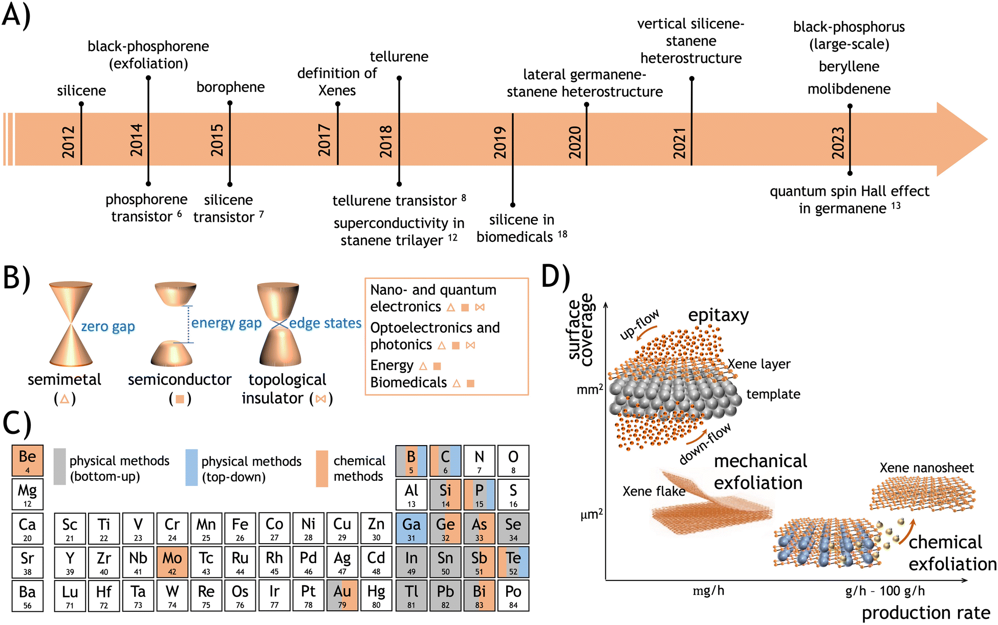 | ||
Fig. 1 (A) Roadmap of the Xenes, including the debut of each Xene (on top of the arrow) and the technological and scientific achievements (on the bottom of the arrow). (B) Band structures classified into three groups: semimetal (△), semiconductor with a gap (■), and topological insulator (![[X triangles, left, right]](https://www.rsc.org/images/entities/char_22c8.gif) ). (C) List of elements in the periodic table that can be configured as Xenes, with one or more listed methods. (D) Graph of the Xene production methods vs. production yield and areal coverage. ). (C) List of elements in the periodic table that can be configured as Xenes, with one or more listed methods. (D) Graph of the Xene production methods vs. production yield and areal coverage. | ||
| Group | Xene | Method | Scheme | Substrate [temperature] | Source |
|---|---|---|---|---|---|
| AE | Beryllene | Chem | Liquid exfoliation | Be powder20 | |
| TM | Molybdenene | Chem | Liquid exfoliation | MoS2 and graphene21 | |
| NM | Goldene | Phys | Exchange intercalation + selective etching | Ti3SiC2 | |
| Ti3AuC222 | |||||
| III | Borophene | Phys | Deposition (epi) | Ag(111)23,24 | |
| Ag(110)25 | |||||
| Ag(100)26 | |||||
| Cu(111)27 | |||||
| Au(111)28 | |||||
| Al(111)29 | |||||
| Ir(111)30 | |||||
| Gallenene | Phys | Solid–melt exfoliation | GaN, Si, GaAs31 | ||
| Indiene/indenene | Phys | Intercalation (epi) | SiC(0001)32 | ||
| Thallene | Phys | Deposition and segregation (epi) | Si(111)33 | ||
| IV | Silicene | Phys | Deposition (epi) | Ag(111)1 | |
| Ir(111)34 | |||||
| ZrB2(0001)35 | |||||
| ZrC(111)36 | |||||
| Ru(0001)37 | |||||
| HOPG38 | |||||
| Pb(111)39 | |||||
| MoS240 | |||||
| G/6H-SiC(0001)41 | |||||
| α-Al2O3(0001)42 | |||||
| CaF2/Si(111)43 | |||||
| Segregation (epi) | ZrB2(0001)/Si(111)4 | ||||
| Intercalation (epi) | G/Ru(0001)44 | ||||
| hBN/ZrB2(0001)/Si(111)45 | |||||
| Chem | Topotactic deintercalation | Sr,Gd,Eu/Si(111)46–48 | CaSi249 | ||
| Germanene | Phys | Deposition (epi) | Au(111)50 | ||
| Pt(111)51 | |||||
| Al(111)52 | |||||
| MoS253 | |||||
| Cu(111)54 | |||||
| AlN/Ag(111)55 | |||||
| Sb(111)56 | |||||
| HOPG57 | |||||
| Ag(111)58,59 | |||||
| Segregation (epi) | Pt/Ge(110)60 | ||||
| Ag(111)61 | |||||
| Al(111)62 | |||||
| Ag0.9Al0.1(111)63 | |||||
| Au(111)64 | |||||
| Intercalation (epi) | MoS265 | ||||
| Chem | Topotactic deintercalation | CaGe266 | |||
| Stanene | Phys | Deposition (epi) | Bi2Te3(111)67 | ||
| Ag(111)68 | |||||
| Cu(111)69 | |||||
| Au(111)70,71 | |||||
| Sb(111)72 | |||||
| Pd(111)73 | |||||
| InSb(111)74 | |||||
| PbTe(111)75 | |||||
| Plumbene | Phys | Deposition (epi) | Fe/Ir(111)76 | ||
| Au/Pb(111)77 | |||||
| Segregation (epi) | Pd(111)78 | ||||
| V | Black phosphorene | Phys | Physical exfoliation | BP79 | |
| Pulsed laser deposition | Mica80 | ||||
| Chem | Chemical exfoliation | BP81,82 | |||
| Epi-(blue)phosphorene | Phys | Deposition (epi) | Au(111)83 | ||
| Arsenene | Chem | Chemical exfoliation | As84 | ||
| Antimonene | Phys. Chem | Deposition (epi) | PdTe285 | ||
| Chemical vapor deposition | Ge86 | ||||
| Bismuthene | Phys | Deposition (epi) | SiC(0001)87 | ||
| Ag(111)88 | |||||
| VI | Selenene | Phys | Deposition (epi) | Si(111)89 | |
| Tellurene | Phys | Deposition (epi) | Mica90 | ||
| Self-assembling from SiTe | Sb2Te391 | ||||
| Chem | Chemical exfoliation (hydrothermal synthesis) | Te-I92 | |||
| Hetero-structures | Graphene/silicene (v) | Phys | Intercalation (epi) | Ru(0001)44 | |
| MoS2/silicene (v) | Phys | Deposition (epi) | MoS240 | ||
| Graphene/germanene (v) | Phys | Deposition and segregation (epi) | Ag(111)93 | ||
| Stanene/germanene(l) | Phys | Deposition and segregation (epi) | Ag(111)94 | ||
| Silicene/stanene (v) | Phys | Deposition (epi) | Ag(111)95 | ||
| Stanene/silicene (v) | Phys | Deposition (epi) | Ag(111)95 | ||
| hBN/silicene (v) | Phys | Intercalation (epi) | ZrB2(0001)/Si(111)96 |
Nowadays, it is apparent that diverse methodologies can be implemented to synthesize Xenes by design, and these generally encompass physical and chemical methods depending on whether Xene formation is dictated by a physical process (nucleation and growth or mechanical cleavage) or is mediated by a chemical reaction or treatment. The former one mainly consists of diverse epitaxial schemes as a bottom-up approach for Xene growth. We also add some notable examples of top-down exfoliation of Xene nanosheets from bulky crystals, such as the case of (black-) phosphorene from black phosphorus (BP),97 which can also be considered a physical method. The chemical route mainly involves topotactic deintercalation from layered compounds, liquid exfoliation enabled by chemical solvents, or thermally induced phase separation.
The different approaches to Xene synthesis are schematically illustrated in Fig. 1D as a function of the surface coverage scale and the production rate, defined as the areal extent that is uniformly wet by a single-layer or multilayer Xene and the rate at which the weight of an individual Xene is produced for a given synthesis method, respectively. Generally, epitaxial methods, as a bottom-up approach to crystal growth, result in a superior control of the surface structure gained from the atomic control of the growth evolution. In addition, the epitaxial methods are effective in gaining a large-area coverage experimentally demonstrated up to cm2 scale but virtually extendable to the wafer scale depending on the spatial constraints affordable in the ultra-high vacuum (UHV) production condition. The overall yield in terms of massive production is quite limited, and the cost per production item is generally high owing to the use of the UHV equipment. Conversely, chemical methods may yield cost-effective massive production with micro-scaled flakes eventually embodied in a framework, thus leading to a considerably larger production yield but scarce control of the structural features in the obtained framework of nanosheets. Exfoliation (either physical through mechanical cleavage, for instance, or chemical through solution-induced delayering) as a top-down approach to the derivation of Xene nanosheets is limited by the extraction of microscaled flakes with good-to-high structural quality, low cost, low yield, no scalability, and availability of the host layered materials. Further details on scalability and production issues are discussed in Section 4.
From this background, we review Xene synthesis methodologies. Unlike other reviews on the topic, our focus here is on the synthesis schemes enabling the isolation of Xenes on substrates or as freestanding membranes, and all along this way, how they can be engineered and/or adapted to fabricate new materials (e.g. heterostructures) or optimize the existing ones and to enable technology transfer to a functional application.
2. Physical methods for Xene Synthesis
Physical methods for Xene synthesis encompass bottom-up and top-down approaches. The former one is concerned with epitaxial crystal growth, whereas the latter one mainly consists of an exfoliation scheme that does not involve the mediation of chemical reactions.Epitaxy is a bottom-up approach for producing an overlayer on the precisely oriented surface of a given substrate. Etymologically, the term comes from the Greek roots “epi” and “taxis,” meaning “above” and “order”, respectively, and thus refers to the growth of an ordered single crystal above a substrate serving as a template. Thus, the epitaxial character of a crystal is reflected in the monocrystalline nature of the grown layer consistent with the normal direction of the growth surface. In this framework, diverse (physical) epitaxial schemes can be implemented,5 which span from the bare molecular beam deposition (where the X atom flux impinges on the growth surface through a vacuum environment) to the top-to-bottom intercalation (where the deposition is mediated by a buffer layer on the growth surface) to the bottom-to-top segregation (where the X atoms are supplied by the substrate through a buffer interface layer); see Fig. 2 for an overview of the different schemes. An essential point for all the approaches is the role of the template in Xene's growth. A template, namely the surface of the epitaxial substrate, exhibits an atomic lattice that is commensurate with an energetically admitted Xene structure; namely, the template and the Xene surface unit cells have the least common multiple. Finally, echoing the concept of the van der Waals heterostructures, we pay attention to the particular case of epitaxial Xene heterostructures, where different Xenes are vertically or laterally interfaced. A list of the epitaxial methods and related experimental cases is given in Sections 2.1–2.3. Section 2.4 is dedicated to physical exfoliation schemes adapted to specific cases.
 | ||
Fig. 2 Physical methods. Xene epitaxy by deposition: (A) simplified sketches of the direct growth and intercalation-mediated growth. (B) Evolutive scanning tunneling microscope (STM) images of the silicene formation by direct growth on Ag(111) at 0.1 ML, 0.3 ML, and 1 ML coverage (from left to right), adapted from ref. 98 (with permission from IOP). (C) Non-planar Xene structures: buckled phases in silicene (4 × 4) and  phases indicating the coincidence relationship with the surface unit cell), adapted from ref. 98 (with permission from IOP), and β12 and χ3 phases of borophene, adapted from ref. 99 (with permission from Springer-Nature). Xene epitaxy by segregation: (D) simplified sketches of the segregation through a buffer layer and topotaxy. (E) STM images (with two different scales) of silicene spontaneously grown by segregation from a Si substrate through a (0001)-oriented ZrB2 buffer layer (top), adapted from ref. 4 (with permission from APS through a Creative Commons Attribution 3.0 License) and LEED pattern with STM image of germanene segregation from Ag(111) thin film on Ge(111) substrate (bottom), adapted from ref. 61 (with permission from IOP). (F) Scanning transmission electron microscope images of silicene layer in CaSi2 formed by segregation from a Si substrate and topotactic reaction with a Gd overlayer. Adapted from ref. 47 (with permission from Springer-Nature): top-view (left), cross-section view of bulk and monolayer GdSi2 (right); Xene heterostructures: (G) Xene and transition metal dichalcogenide (TMD) hybrid heterostructure: MoS2/silicene with Si grown on a MoS2 surface, adapted from ref. 40 (with permission from Wiley). (H) Silicene–stanene heterostructures by sequential epitaxy on Ag(111), representative sketches (left) and corresponding LEED patterns (right), based on results from ref. 95. (I) Growth of lateral germanene-stanene heterostructure by atomic segregation from a Ge substrate through a (111)-terminated epi-Ag layer that is partially covered by stanene domain grown by direct growth according to the process schematics (top) and the atomically resolved topography of the stanene domain laterally surrounded by germanene (bottom), adapted from ref. 94 (with permission from Wiley). phases indicating the coincidence relationship with the surface unit cell), adapted from ref. 98 (with permission from IOP), and β12 and χ3 phases of borophene, adapted from ref. 99 (with permission from Springer-Nature). Xene epitaxy by segregation: (D) simplified sketches of the segregation through a buffer layer and topotaxy. (E) STM images (with two different scales) of silicene spontaneously grown by segregation from a Si substrate through a (0001)-oriented ZrB2 buffer layer (top), adapted from ref. 4 (with permission from APS through a Creative Commons Attribution 3.0 License) and LEED pattern with STM image of germanene segregation from Ag(111) thin film on Ge(111) substrate (bottom), adapted from ref. 61 (with permission from IOP). (F) Scanning transmission electron microscope images of silicene layer in CaSi2 formed by segregation from a Si substrate and topotactic reaction with a Gd overlayer. Adapted from ref. 47 (with permission from Springer-Nature): top-view (left), cross-section view of bulk and monolayer GdSi2 (right); Xene heterostructures: (G) Xene and transition metal dichalcogenide (TMD) hybrid heterostructure: MoS2/silicene with Si grown on a MoS2 surface, adapted from ref. 40 (with permission from Wiley). (H) Silicene–stanene heterostructures by sequential epitaxy on Ag(111), representative sketches (left) and corresponding LEED patterns (right), based on results from ref. 95. (I) Growth of lateral germanene-stanene heterostructure by atomic segregation from a Ge substrate through a (111)-terminated epi-Ag layer that is partially covered by stanene domain grown by direct growth according to the process schematics (top) and the atomically resolved topography of the stanene domain laterally surrounded by germanene (bottom), adapted from ref. 94 (with permission from Wiley). | ||
In parallel, let us also mention that Xenes derived by physical methods are usually addressed by a characteristic number of experimental techniques that are markedly surface-sensitive and mainly operate under UHV conditions (namely, the environment where the Xenes are usually grown).100 Scanning tunneling microscopy/spectroscopy (STM/STS) and atomic force microscopy (AFM) are utilized to obtain detailed information on the atomic-level resolution of surface structures and spatially local electronic properties. The STM images are obtained through a tunneling current reflecting a local electronic structure near the Fermi energy. Thus, it is crucial to examine whether the STM images have any sample bias voltage dependence for geometrical determination from the STM images. AFM images are obtained by attractive or repulsive force between the tip and the surface, thus directly reflecting the atomic position. For both methods, knowing the structural relationship between Xene and the substrate is usually tricky unless a Moiré structure is observed in the STM images. Low-energy electron diffraction (LEED) is convenient for examining the uniformity and symmetry of Xene (2, 3, 4, or 6 fold) and the structural relationship between Xene and the substrate, such as azimuthal rotation angles and the ratio of lattice constants (commensurate or incommensurate). Reflection high energy electron/positron diffraction (RHEED/RHEPD) and surface X-ray diffraction (SXRD) are also powerful tools for identifying the symmetry of the geometrical structure and its height from the substrate. Auger electron spectroscopy (AES), X-ray photoemission spectroscopy (XPS), and core-level photoemission spectroscopy (PES) provide a coverage or compositional ratio as well as an impurity analysis. PES and Raman spectroscopy are used to examine the local bonding and crystal structure, respectively. Raman spectroscopy is a powerful tool for identifying silicene and germanene because of the specific peaks observed, similar to graphene. In this respect, Raman spectroscopy allows for discriminating the single layer and multilayer regime in terms of a red shift due to a tensile strain and a blue shift due to compressive strain101 and for precisely determining the thickness of the Xene sheets from the relative separation between the main Raman spectral features, such as in the case of the B2g and A2g modes of exfoliated BP flakes.102
Furthermore, angle-resolved photoemission spectroscopy (ARPES) provides an valence band structure near the Fermi energy. Usually, these experimental techniques are paralleled and supported by ab initio calculations based on density functional theory (DFT), which allows for the interpretation and rationalization of the experimental data.103 In particular, following a conventional surface science analytical approach, the theoretical modeling serves as a throughput to the interpretation of experimental data, e.g. in the identification of the atomic structure and local density of states from STM/STS measurements (see, for example, ref. 23 and 99 for the case of borophene), the electronic band structure is close to the Fermi level from ARPES measurements (see, for example, ref. 69 and 104), and the characteristic vibrational modes from Raman spectra.105
2.1 Deposition
Xenes can be grown by (1) direct deposition of X atoms in vacuo on a supporting substrate, or (2) intercalation of the evaporated X beam, e.g. in between a buffer layer and the substrate.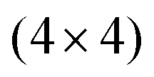 ,
,  , and
, and  ,1,108–110 see Fig. 2C. The alternation of these surface phases is a rate-limited process dictated by growth kinetics, e.g., by varying the substrate temperature during growth. Diverse silicene phases can coexist although each phase proportion is temperature-dependent.
In contrast, single-phase selection can be obtained by Ag surface engineering via atomic Sn decoration and buffering.111 Stepping forward to the second and multiple layers leads to the emergence of a unique type of surface order, denoted as the  , in a three-dimensional (3D)-like growth mode, namely with the topmost domains nucleating before the underlying layers are completed. This reconstruction was interpreted either as an intrinsic silicene feature or as a superstructure of segregated Ag atoms through a diamond-like silicon film. The two pictures were reconciled within the argument of temperature-dependent activation of Ag atom segregation101,112 according to which silicene grows multilayer only in a narrow temperature window where Ag diffusion is hindered.
Another example of allotropism is borophene (2D boron) as epitaxially grown on Ag(111). In the MBE scheme, the boron atoms are thermally evaporated onto the substrate temperature at a given temperature ranging from nearly 300 °C to 380 °C to avoid clustering.99,113 Taking Ag(111) as a representative substrate again, two ordered phases qualify the growth of borophene, which correspond to the β12 and χ3 model structure of borophene conceptual structure, see Fig. 2C (bottom).114 Based on first-principles calculations, borophene is made possible by removing B atoms from the pristine triangular flat sheet, thus creating an atomic vacancy.115 This event can, therefore, generate a handful of possible 2D lattice configurations quantitatively identified by the global structural parameter h (i.e., the ratio between vacancy sites and the available atomic site in a unit cell) and the coordination number c for each B atom in the lattice. The two experimentally observed phases coincide with (h,c) = (1/6,5) and (h,c) = (1/5,4) for the β12 and χ3 structures, respectively.99
Metal surfaces may also serve as catalyzers for the growth of Xenes. This is the case of the so-called blue phosphorene, namely a 2D allotrope of phosphorus with a rhombohedral structure at variance with the more popular black phosphorene with an orthorhombic structure, where the host Au(111) surface selectively facilitates the dissociative absorption of the P4 molecular beam, supplied by the sublimation of a BP matrix in the crucible of a Knudsen cell. The so-dissociated P atoms self-assemble on a herringbone-reconstructed Au(111) surface with a flower-like motif assigned to the Au-P framework model, where substrate Au atoms decorate the blue-phosphorene domain.83,116 More recently, within the same scheme of direct deposition from the vapor phase, epitaxial phosphorene was grown on Cu(111), thereby providing a large-area coverage.117,118 The epitaxy of blue phosphorene was initially regarded as the path to bypass the limited scalability of the mechanically exfoliated black phosphorene from BP. However, recently, large-area production of black phosphorene was reported using pulsed laser deposition.80 Using a similar method, Xene growth was demonstrated on non-metallic substrates serving as templates. Among these are 2D layered crystals, as in the case of the silicene or germanene growth on MoS240,53 or stanene growth on Bi2Se3,67 or single-crystal large-gap crystals, as in case of the growth of silicene on α-Al2O3(0001),119 graphene/SiC(0001),41 CaF2/Si(111),43 and bismuthene on SiC(0001).87 Recently, in addition to the 2D-layered sheets, 1D- nanoribbon of silicene was synthesized on Ag(110) surface.120 The geometrical structure is determined to be a pentagon-related structure, which is theoretically proposed to induce p-wave superconductivity and is expected for the emergence of spin-polarized Majorana zero-modes.121
2.2 Segregation
At variance with the direct deposition through MBE, Xene epitaxy can occur the other way around through X atoms diffusing from the substrate to the surface, namely by segregation from the substrate with or without the presence of a buffer layer (Fig. 2D). An example of this mechanism is the so-called atomic segregation epitaxy (ASE), which involves fewer experimental parameters than deposition methods. Basically, only three ingredients are mandatory within the ASE scheme of operation: the substrate X supplying the X atoms through a buffering layer, the buffer layer serving as a template for the desired Xene growth, and careful control of the substrate temperature (see Fig. 2D and E). In this framework, the temperature of the sample can be uniformly controlled, thus making it relatively straightforward to fabricate highly crystalline 2D materials on an ultra-large scale and benefiting from the segregation flux. The pristine sample, consisting of the X substrate with the buffer layer, is heated at temperatures that are relatively higher than those in the deposition scheme (e.g. T > 645 °C for silicene on ZrB2(0001)/Si(111),126T > 480 °C for germanene on Ag(111),61 and T > 430 °C for germanene on Al(111)62), thereby triggering atomic (X) segregation to the very surface level where the hot (mobile) X atoms self-organize according to the crystalline match with the buffer layer. In this method, the X atoms melt in bulk at high temperatures or diffuse through crystal defects in the buffer layer, such as grain boundaries. Therefore, the most energetically stable 2D materials can spontaneously be prepared on UHV-treated substrates. A pioneering study in this respect was carried out in 2012 by Fleurence et al. during the research process, in which atomic layer silicene was fabricated on metallic zirconium diboride (ZrB2) thin films epitaxially grown on Si(111) by ASE; see Fig. 2E top panel.4 The lattice constant of silicene has a magic mismatch to that of ZrB2(0001). This is a critical aspect of the epitaxial growth as long as lattice matching induces strong bonding between silicene and ZrB2, which may affect the properties of free-standing silicene. Nevertheless, the ASE method has demonstrated the size of the grown silicene up to the cm2 scale, which can be made even larger depending on the design of the growth system.In the ASE method, lattice matching is important for fabricating a single-crystal film on a crystal substrate. Ag crystals are one of the best candidates for lattice matching with Ge crystals, with a lattice constant ratio of 3![[thin space (1/6-em)]](https://www.rsc.org/images/entities/char_2009.gif) :4. Experimentally, Ag(111) thin films with high crystalline quality were grown on Ge(111).127–129 In 2018, germanene synthesis using the ASE method was reported for Ag(111) thin films on the Ge(111) substrate.61 The lattice size of germanene is close to free-standing germanene,130 and the lattice matching between germanene and Ag(111) is extremely large, with a length of 5.35 nm, corresponding to a
:4. Experimentally, Ag(111) thin films with high crystalline quality were grown on Ge(111).127–129 In 2018, germanene synthesis using the ASE method was reported for Ag(111) thin films on the Ge(111) substrate.61 The lattice size of germanene is close to free-standing germanene,130 and the lattice matching between germanene and Ag(111) is extremely large, with a length of 5.35 nm, corresponding to a  superstructure (see Fig. 2E, bottom panel). The germanene prepared by ASE is significantly different from the germanene prepared by MBE, even on the same Ag(111) surface. This is mainly because the relatively lower sample temperature is restricted to prevent the dissolution of Ge atoms into Ag(111) in the MBE method.58,131,132 Specific phonon modes in germanene have been identified by tip-enhanced Raman spectroscopy (TERS) combined with STM imaging.133 Subsequently, graphene-capped Ag(111)/Ge(111) samples were also used for interfacial germanene synthesis, which was also confirmed by Raman spectroscopy.93 Recently, structural models of germanene with
  and
and  reconstructions on Ag(111) are proposed using STM, surface X-ray diffraction, and DFT calculations.59
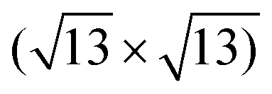
Because the unit cell sizes of Au and Al are similar to those of Ag, Al(111) and Au(111) films with high crystalline quality have also been fabricated on Ge(111). Ge atoms in the Ge(111) substrate indeed dissolve into the Al and Au thin films and segregate on the Al(111) and Au(111) surfaces. For Al(111) thin films, segregated Ge atoms form germanene with a (2 × 2) superstructure matching with the Al(111)(3 × 3) unit cell,62 which is identical to the direct deposition case. In the latter method, there are two germanene phases of (2 × 2) and  with very similar Ge coverages,134 resulting in a mixed phase with the same layer. Conversely, the ASE method readily leads to a (2 × 2) single phase.62 For Au(111) thin films on a Ge(111) substrate, segregated Ge atoms form (5 × 8) reconstruction, which is slightly different from germanene prepared by direct deposition epitaxy.50,135 In 2019, with a similar approach, plumbene was synthesized using a PbxPd1−x alloy (111) surface on Pd(111).78,136 Pd is one of the best elements for Pb surface segregation because Pb–Pd alloys are thermally very stable at temperatures higher than 1200 °C for the PbxPd1−x alloy (x < 0.12).
Another approach to segregation-assisted epitaxy of Xenes is the topotaxial growth of silicene and germanene embedded in Zintl compounds MX2 (where M is a rare earth element such as Eu or Gd, or Sr, and X is Si or Ge) on Si or Ge substrates, respectively. In detail, a pre-deposited nanoscale M film encounters segregation of the X atom from the substrate and, under tailored constraints, reacts with the X atom by forming the layered MX2 compound where the X atoms self-arrange in a planar sheet between two top and bottom M layers46–48 (see Fig. 2F). Thus, the so-functionalized Xene sheet is affected by the surrounding environment. Consequently, owing to magnetic anisotropy or dipolar interactions, it displays a magnetic order, e.g., ferromagnetism, at the 2D level.
Although not directly associable with segregation schemes, as reported above, it is worth mentioning the self-assembling approach to the epitaxial growth of α-tellurene results from the Te atomic chains that are released from SiTe grown on a Sb2Te3 template under non-equilibrium conditions.
2.3 Epitaxial growth of heterostructures
We can classify two types of heterostructures: vertical and lateral heterostructures. The former type may appear as hybrid and pure Xene heterostructures. Hybrid Xene heterostructures incorporate a Xene layer grown on a 2D layered non-Xene substrate (single or multilayered) template by benefitting from van der Waal epitaxy or selective hybridization at the surface. However, a pure Xene heterostructure displays a sequence of two different Xene layers. Relevant cases in this respect are stanene on Bi2Te3, and silicene or germanene on MoS2.53,67,137 In both cases, the Xenes display a regularly buckled structure in which the lattice constant coincides with that of the substrates with an overall metallic character.Within the hybrid Xene heterostructures, Chiappe et al. reported the growth of 2D Si nanosheets on MoS2 surfaces examined by STM and STS measurements supported by DFT calculations, ending up in silicene with a metallic character40 and bending of the MoS2 electronic bands138 (see Fig. 2G). On the other hand, silicene layers on MoTe2, GaS, and GaSe are predicted to be gapless semiconductors, with preserved Dirac cones at the K points.139 Other similar systems, such as germanene on MoS2,53,65 antimonene on PdTe2,85 silicene nanosheets on graphite,38,140 and germanene islands on graphite,57 were also intensively studied. The cases of Ge and Si deposition on MoS2 were reconsidered in terms of Ge and Si atom intercalation through the MoS2 layer.65,141 The intercalation path can be driven by thermally activated crossing through structural defects in the layered substrate; thus, it depends strictly on the quality of the MoS2 substrate. Similarly, Sn deposition on TiS2 was examined by STM because Sn atoms are intercalated mainly from the step edge.142 The structural defects and interstitial atoms in the layered TiS2 substrate affect the intercalation migration process.
For a vertical heterostructure, a stable silicene-graphene heterostructure is prepared on Ru(0001) by silicon deposition on graphene/Ru(0001), as well as a silicene-hBN monolayer heterostructure on ZrB2(0001) film on Si(111), with intercalation of Si atoms in between graphene or hBN monolayer on substrates.41,44,45 Li et al. observed that graphene plays the role of a capping layer for silicene.44 Wiggers et al. demonstrated by core-level photoemission spectroscopy that the hBN monolayer prevents oxidation of underlying silicene at least for an hour, acting as a capping layer despite its monolayer thickness.45 Titter et al. used a few graphene layers as a capping layer to encapsulate silicene.143 Within the same vertical heterostructure scheme, Dhungana et al. demonstrated the stacking of silicene on stanene and vice versa by sequential epitaxial growth on a Ag(111) substrate, thereby paving the way to an artificial pile-up of diverse Xenes on a superlattice structure (see Fig. 2H).95
For the lateral heterostructure, the first attempt was reported by Kiraly et al. in 2015, in which the sequential deposition of carbon and silicon on Ag(111) resulted in the synthesis of both lateral and vertical graphene–silicon heterostructures.144 Graphene–borophene heterostructures are also demonstrated on Ag(111) using a similar method, reporting on the synthesis of both lateral and vertical interfaces.145 The first achievement of a true lateral heterostructure with epitaxial Xenes was provided by Ogikubo et al. in 2020 in which germanene-stanene lateral heterostructures are synthesized on Ag(111) using the combination of MBE and ASE epitaxies.94 (see Fig. 2I).
2.4 Physical exfoliation
Top-down approaches are concerned with Xenes being exfoliated, extracted, or reduced from a bulky phase instead of being atomically grown and self-organized on a substrate, and may involve either physical operations (e.g. mechanical cleavage) or chemical treatment (e.g. liquid phase exfoliation). Thus far, they include (black) phosphorene (a single layer of black phosphorus), gallenene, tellurene, and beryllene (see Table 1). Mechanical exfoliation is the pristine way graphene and other consolidated 2D materials were extracted from bulky crystals. This was also the case of phosphorene, originally referred to as the 2D single-layer derived from a black-phosphorus crystal, namely the phosphorus allotrope displaying an orthorhombic structure in a layered solid. Multilayered phosphorene (from a single layer to a few nm) was initially derived through mechanical exfoliation using scotch tape adhesion to bulk black-phosphorus crystals. The so-obtained flakes were integrated into a transistor device structure with p-type conductivity (as illustrated in the roadmap in Fig. 1A).6Taking advantage from the liquid metal character of gallium at room temperature, atomically thin gallenene (2D gallium) sheets were obtained by a solid–melt interface exfoliation method consisting of a stamp of a Ga droplet, kept at a temperature slightly higher than its melting temperature, onto a SiO2/Si wafer brought into contact with the surface of the Ga droplet.31 The lower temperature at the SiO2–Ga interface results in the solidification of the surface Ga layers, thus effectively leading to the exfoliation of an mm-scaled sheet from the melt.
3. Chemical methods for Xene synthesis
The top-down approaches in tetrel chemistry covering silicene and germanene, as well as the huge spectra of their derivatives, are well known. Indirect methods based on chemical exfoliation, so-called topotactic reaction or deintercalation, are applied to compounds containing hexagonally arranged layers of silicon and germanium, which resemble those of Si(111) or Ge(111) bilayers from bulk silicon or germanium crystallized in the diamond structure. These compounds, known as a Zintl phase with the general formula of MX2, where M is typically calcium or europium, and X is silicon or germanium in the form of the hexagonally packed layer with in-plane bonds, are key precursors for topotactic (also named topochemical) conversion to silicene/germanene and their derivatives. Topotactic or topochemical reactions are generally chemical processes that lead to chemical changes without significant structural changes in the material. Zintl phase conversion to silicene/germanene is an example of such a chemical process. This type of Zintl phase has been known for decades, and the existence of CaSi2 was already reported in the middle of the 19th century, together with its topotactic conversion. The silicon-germanium alloy forms a continuous solid solution system where germanium can also be substituted up to about 25 at% tin. The topochemical deintercalation of calcium layers from calcium disilicide, calcium digermanide, and their solid solution were reported using different etchant and electrochemical methods, typically providing covalent functionalized silicene and germanene derivatives.49 The synthesis of non-functionalized silicene and germanene is much rarer, and such materials are extremely reactive because covalent functionalization leads to the stabilization of the 2D pocked honeycomb structure. The mechanism of CaGe2 chemical exfoliation together with formed flakes is shown in Fig. 3A and B.66 Chemical exfoliation is nicely documented by X-ray diffraction, where calcium digermanide is at low temperature by reaction with acid converted to hydrogentated germanene (germanane) with significantly higher lattice spacing (Fig. 3C). | ||
| Fig. 3 Chemical methods. Topotactic deintercalation. (A) Reaction scheme of calcium-selective etching from CaGe2 Zintl phase by hydrochloric acid. (B) Flakes of germanane obtained from CaGe2. (C) X-ray diffractogram of CaGe2 before and after chemical exfoliation. (Reprinted from ref. 66 under permission from ACS). (D) Reaction mechanism of CaGe2 exfoliation and functionalization by alkylhalogenides. (Reprinted from ref. 146 under permission from ACS). (E) Scheme of benzylsilicene synthesis by reaction of calcium disilicide with benzylbromide. (Reprinted from ref. 147 under permission from ACS). (F) Photoluminescence of methylated germanene with and without the presence of moisture and corresponding photoluminescence spectra. (Reprinted from ref. 148 under permission from ACS). Liquid-phase exfoliation. Electrochemical exfoliation of BP to phosphorene using anodic exfoliation (G) and cathodic exfoliation using (H) tetrabutylammonium hydrogensulfate. (Reprinted from ref. 149 under permission from Elsevier). Ultrasonication setup for black phosphorus under an inert atmosphere (I). Photo of dispersion in NMP before and after centrifugation (J). Concentration of exfoliated BP in various solvents (K). Dependence of concentration on solvent surface tension (L). (Reprinted from ref. 150 under permission from ACS). | ||
Chemically derived Xenes differ from epitaxial Xenes in terms of characterization methods and are commonly investigated by several material characterization techniques; see, for example, ref. 130,132. The methods of analysis depend strongly on the composition of the Xenes. In general, XPS is used to determine the surface chemical composition and can be combined with energy (EDS) or wavelength dispersive spectroscopy (WDS) alongside various electron microscopy methods. However, significantly greater information depth provides more “bulk-like” information about elemental composition, but extreme spatial resolution of chemical composition can also be achieved. Electron microscopy-related methods with outstanding spatial resolution (especially transmission microscopy in combination with EDS or electron energy loss spectroscopy (EELS) provide information with extremely high lateral resolution theoretically down to single atoms but obtained informations about chemical bonds are limited. XPS has limited spatial resolution because it works with X-ray as an excitation source. However, high spectral resolution allows for obtaining detailed information about the bonds of individual atoms. The XPS method is crucial for Xene surface chemistry analysis, including the identification of the type and degree of surface functionalization as well as the type of bonds between Xene and surface atoms. This method is highly complementary to the vibration spectroscopy method, as infrared spectroscopy can provide complex information about surface chemistry. Valuable informations are obtained by vibrational spectroscopy methods, namely infrared (FT-IR) and Raman spectroscopy, where tip-enhanced and related techniques can provide information with lateral resolution even beyond the diffraction limit, such as tip-enhanced Raman spectroscopy (TERS), scanning near-field optical microscopy (SNOM) and related techniques. As said for the case of mechanically exfoliated BP flakes, Raman spectroscopy is practical in readily determining the thickness from the separation of the characteristic vibrational modes, e.g. the case of the A1 and E2 modes in tellurene.151 For infrared spectroscopy, various methodologies are employed depending on the absorption properties of the analyzed material (such as diffuse or specular attenuated total reflectance, or optical transmittance methods). In particular, the diffuse reflectance (DRIFT) method can provide valuable information even for highly absorbing samples in a broad spectral range using dilution with KBr and measuring temperature dependence by operando high-temperature cells. The FT-IR method is complementary to Raman spectroscopy, which offers a high spatial resolution. However, in Raman spectroscopy the information about chemical modification is more limited than that obtained from the infrared spectroscopy methods. Beyond these well-known methods, other techniques, such as combustion elemental analysis, thermal analysis combined with evolved gas analysis, or solid-state nuclear magnetic resonance (NMR), can provide valuable insights and a more detailed view of particular aspects of material chemistry and surface functionalization. For Xenes prepared by applying top-down methods, X-ray diffraction provides crucial information about phase composition, the number of layers in the system, and lattice parameters. The layer distance is strongly influenced by the functionalization group, and these effects can be clearly resolved by X-ray diffraction. Surface morphology analysis is performed using various probe and electron microscopy methods.
Although electron microscopy (scanning electron microscopy and transmission electron microscopy) provides valuable information about morphology and the associated methods give information about material composition, direct thickness obsevation and estimation the number of layers requires probe microscopy methods. AFM is generally used to obtain information about flake thickness distribution, while conductive and Kelvin force methods provide additional information about surface chemistry and electronic properties. Compared to “bottom-up” physical methods, STM is not broadly used for characterization of exfoliated Xenes due to surface defects and contaminants originating from “top-down” chemical methods.
In what follows, we address specific examples of topotactic deintercalation with a focus on silicene, germanene, and recent advances in other Xenes (Section 3.1), and then we consider alternative chemical approaches to Xene synthesis (Section 3.2) and the case of liquid-phase exfoliation (Section 3.3).
3.1 Topotactic deintercalation
The most common layered Zintl phase, CaSi2, has been well known for many decades and is in a low-purity form used in tone scales in the steel industry. However, the germanium-based counterparts are significantly more novel, and most of the reports originate from the 21st century. The first report on the topotactic formation of the silicene derivatives originated from German chemist Friedrich Wöhler in 1863, who reported the reaction of CaSi2 with cold aqueous hydrochloric acid to form a yellow powder currently known as planar polysiloxene, a silicene derivative with the general formula Si6H3(OH)3,152 as follows:| 3CaSi2 + 6HCl + 3H2O → 3CaCl2 + Si6H3(OH)3 + 3H2 (T ∼ 20 °C) |
| 3CaSi2 + 6HCl → 3CaCl2 + Si6H6 (T ≪ 0 °C) |
Additionally, pure silicene can be synthesized by the topotactic conversion of calcium disilicide. Pure silicene synthesis was reported using the reaction of CaSi2 with SbCl3, producing silicene together with antimony and calcium chloride,160 as follows:
| 3CaSi2 + 2SbCl3 → 3CaCl2 + 6Si + 2Sb |
Compared to silicene and its derivatives, the chemistry of germanene and its derivatives is less investigated. The first topotactic deintercalation of calcium from the CaGe2 structure was reported in 1944.167 The first synthesis of hydrogenated germanene, which is called germanane, was reported by Goldberger significantly later in 2013.66 The strategy used for synthesis is identical to the methods applied to silicane based on low-temperature etching with aqueous hydrochloric acid according to the following reaction:
| CaGe2 + 2HCl → 2GeH + CaCl2 (T < 0 °C) |
Borophene is the only other Xene prepared by topotactic reactions. Similar to Zintl phases, many diborides with AlB2 structure consist of honeycomb layers of boron atoms with metal atoms arranged in between, with the most well-known example MgB2. The topotactic exfoliations of MgB2 and other diborides were reported by several groups. Zhang reported the use of I2 in acetonitrile-producing Mg0.22B2 nanosheets.176 Additionally, sonication experiments produce Mg deficient borophene-like structures.177 Chemical removal of cations led similarly to silicene/germanene chemistry to hydrogen-terminated surfaces. The chemical etching of Mg from MgB2 has been reported to produce hydrogen-terminated borophene.178 Chemical etching has also been reported for different borides, such as YCrB4, to produce hydrogen-terminated borophene nanosheets.179 Cationic resins are used by several groups to bind cations during selective topotactic etching to enhance the speed of conversion. Compared to the tetrel group, borophene and its derivatives possess significantly higher reactivity, and a significantly lower number of publications have been reported on the topotactic formation of borophene and its derivatives.
3.2 Thermal deintercalation and other chemical methods
Zintl crystals, such as CaSi2, are a good platform for deriving silicene by thermally decoupling the Ca from the silicene plane upon differential thermal treatment. This approach relies on the different boiling temperatures of Ca (1484 °C) and Si (2900 °C) constituting planes so that silicene planes can already be de-alloyed from CaSi2 at 900 °C.180 A thermally induced transformation was recently proven to be the mechanism for the nucleation of molybdenene (2D molybdenum) from MoS2 powder.21 In detail, molybdenene was synthesized by microwave exposure of a mixture of MoS2 and graphene, where graphene serves as a heat absorption catalyst at the interface with MoS2. The so-generated microwave power melts MoS2 (loosen bonds) when the temperature reaches its melting point (Tm = 1185 °C) and results in Mo–S bond breaking with the release and migration of Mo atoms towards the self-organization of molybdenene whiskers. Released Mo atoms (rich in electrons) respond to such an enormous electric field and migrate through the graphene–MoS2 mixture, constituting a molybdenene layer.Although broadly used in semiconductor science and technology, there are few cases of chemical vapor deposition (CVD) of Xenes on selected substrates that can accommodate both the local Xene nucleation and the pyrolysis of the metal–organic molecular precursor involved in the process. In this respect, antimonene multilayered nanocrystals were grown on a (111)-terminated Ge substrate by benefitting from the surfactant effect of Au nanoparticles on the surface and concomitantly exploiting the SbCl3 precursor dissociation and Cl-induced surface etching.86
3.3 Liquid-phase (or chemical) exfoliation
Exfoliation can be carried out in liquid using appropriate solvents, reagents and conditions. Liquid-phase or chemical exfoliation has gained interest so far as a method for the cost-effective and scalable production of 2D materials. In this respect, under ultra-sonication, phosphorene was exfoliated by rinsing in selective solvents, usually N-methyl-2-pyrrolidone.181 A similar approach has been recently adopted for the exfoliation of beryllene (2D beryllium), namely upon dispersion of dimethylformamide (DMF) solvent, sonification, centrifugation, and thermal drying in a nitrogen environment.20 No other way is currently reported for the synthesis of beryllene flakes. In addition to mechanical exfoliation, electrochemical-assisted exfoliation is well known for several van der Waals Xenes. This method was mainly applied to black phosphorus-producing high-quality single- and few-layer phosphorene with high aspect ratio.182 Owing to its sensitivity towards oxidation, exfoliation is typically performed in an organic solvent under an inert atmosphere. The electrochemical and mechanical exfoliation are shown in Fig. 3G–L. Electrochemical exfoliation can be performed using an anodic method (Fig. 3G) and a cathodic exfoliation method (Fig. 3H). Mechanical exfoliation was demonstrated for several Xenes. In particular, black phosphorus solvent-assisted mechanical exfoliation has been reported by many authors. Because Xenes are highly sensitive to oxygen and moisture, exfoliation is usually performed in dry organic solvents under a protective atmosphere (Fig. 3I), followed by size selection of exfoliated materials by centrifugation (Fig. 3J). The yield of solvent-assisted exfoliation strongly depends on the solvent's physical properties, such as its surface tension and boiling points (Fig. 3K and L). Topotactic reactions are also applicable to several other Xenes. From the pnictogen group, among the allotropes of phosphorus (arsenic, and antimony) adopting the layered structure, direct exfoliation can be performed either using solvent-assisted methods such as share force milling and ultrasonication or more gentle processes of electrochemical exfoliation, which by intercalation can weaken the layer bonds and provide exfoliated sheets with a significantly higher aspect ratio compared to mechanical exfoliation methods. The synthesis of goldene (2D gold) by chemical exfoliation was also reported recently. It is based on the substitution of silicon in the Ti3SiC2 MAX phase (with M, A, and X being a transition metal, a group A element, and C or N, respectively) by gold and the subsequent selective etching of titanium and carbon.22 This method is suitable for the production of flakes with lateral sizes exceeding 100 nm stabilized by organic surfactants. Within chemical exfoliation processing, we may consider tellurene as derived by the so-called hydrothermal synthesis that was originally developed to synthesize one-dimensional (1D) tellurium nanostructures.183 In this scheme, sodium telluride is added to a solution of polyvinylpyrrolidone (PVP). After dissolution, hydrazine and ammonium hydroxide solution are added as a reducing agent and for pH adjustment, respectively, and the temperature is increased up to 180 °C, thus resulting in dissociated tellurium flakes with a trigonal phase in the solution that can be fished and adapted to substrates. Compared to the 1D tellurium synthesis, the case of 2D tellurene nanosheets is different because the pristine material ratio is carefully adjusted and the reaction time is elongated adequately to yield single crystal 2D flakes with lateral sizes; over 100 μm and thicknesses ranging from monolayer to tens of nm can be obtained.4. Technological viability
For most Xenes, the research scope is limited to a niche investigation because of the lack of viable integration protocols in a technology flow. This is why Xene production should be paralleled by a concomitant effort to develop production and processing schemes that enable the transfer of Xene technology. This section is intended to discuss the technological potential of Xenes in terms of the rich electronic properties (Section 4.1), the path to Xene production standards (Section 4.2), limiting issues in Xene handling (such as the lack of stability under environmental conditions) and related solutions of processing and applications (Section 4.3), and the step towards integration with a future outlook on Xene-related emerging technologies (Section 4.4).4.1 Salient electronic properties
Before entering the details of Xene processing, it is worth paying attention to those physical and chemical properties that distinguish synthetic Xenes from other nano-scaled materials and make them suited for specific target applications. One of the salient features of the Xenes in all their forms and configurations is to display an extremely rich variety of electronic states spanning from metals, to semimetals (either topological or not), 2D topological insulators, and semiconductors. Although the electronic character may vary in the same Xene as a function of the surrounding conditions (e.g. substrate, interface, strain, doping, and capping), to a general view, Xenes can be classified as in Fig. 4A. In detail, several Xenes present a non-trivial topology. These include Xenes in the group IV where, according to the Kane–Mele model,184 the spin–orbit coupling interaction in the Hamiltonian causes the opening of an energy gap state in the Xene body and the emergence of topologically-protected edge states.185,186 This effect is negligible at relatively light atomic mass, namely in graphene, silicene, and germanene (with gaps of 1, 10, and 20 meV, respectively), which behave as semimetals at room temperature, but it becomes sizeable when the atomic mass becomes larger, namely in stanene and plumbene (with a gap of up to 0.42 eV).187 This “topological strength” is expressed with an increasingly darker brown color in Fig. 4A. The same topological character can be found in other “heavy” Xenes, such as bismuthene and antimonene.188 Interestingly, non-trivial topological phases of different physical origins can be induced in the 2D-to-3D transition of the epitaxial film growth. For instance, the α-phase of tin, which recasts as stanene at the single-layer level, becomes a Dirac semimetal or topological insulator in the bulk form depending on the induced epitaxial strain (compressive or tensile, respectively) when grown on InSb.189 Tellurene is a different case in the topological framework. It appears as a semiconductor with a thickness-dependent energy gap (from 1.0 eV in the single-layer to 0.3 eV in the multi-layer),190 but topological Dirac cones are incorporated in its conduction band, and they bear a quantum Hall effect owing to Weyl fermion under extrinsic n-type doping.191 Borophene and recently discovered molybdnene, beryllene, and goldene are metallic, whereas gallenene may have an ambipolar metallic-semiconducting character.31 Other known Xenes (thallene, phosphorene, arsenene, and selenene) are semiconducting.33,79,84,89 Clearly, the electronic character concurs with determining the target application(s) of each Xene along with the configurational layout, namely the form in which the Xene is released for an application function.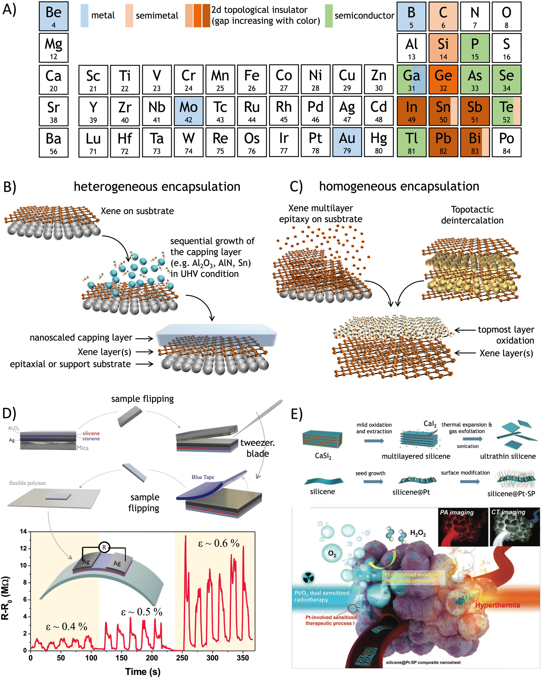 | ||
| Fig. 4 (A) List of the Xenes in the periodic table with the relevant electronic character. (B) Scheme of heterogeneous encapsulation starting from the Xene accommodated on a substrate, and the sequential deposition of a capping layer with nanoscale thickness. (C) Scheme of homogeneous encapsulation resulting from the oxidation of an Xene multilayer derived from epitaxy (left) or from topotactic deintercalation (right). Recent cases of processing and applications of the Xenes after heterogeneous and homogeneous encapsulation. (D) Delamination of silicene from an epitaxial silicene/stanene heterostructure on Ag(111) ending up with an all-around encapsulated membrane to be deposed on a secondary target substrate for the integration into a piezo-resistor device where the resistivity is varied as a function of the applied bending force ε (expressed as a ratio of the radial deformation and the membrane thickness in %). Adapted from ref. 192 (reprinted with permission from Wiley). (E) Topotactic deintercalation of silicene nanosheets from CaSi2 through mild oxidation, sonication, and subsequent functionalization with Pt surface nanoparticles towards the exploitation for theranostic application for the hyperthermal treatment of the tumors. Adapted from ref. 193 (reprinted with permission from Wiley). | ||
4.2 Scalability and massive production
Chemical and physical methods for the Xene synthesis have been developing rapidly in the last decade, and a portfolio of Xenes has been prepared using these same methods. Besides the most well-known group IV elements (tetrels) and group V elements (pnictogens), new members of this family have been reported in the last decade, including tellurene from group VI and borophene from group III elements. These approaches are likely extended in the future to other elements where only theoretical simulations are available for now (see, for instance, the concept of aluminene194). Note that alkali metals from group I were experimentally found to form highly-buckled honeycomb structures when intercalated in between bilayer graphene.195 The limiting factor of industrial use in the real world is the scalability of several Xenes for synthesizing bulk materials, such as BP, or its high price (such as germanium). However, recent progress on the pulsed laser deposition of BP holds promise regarding production scalability.196 In some applications, such as electronics, only a minute amount of active material is needed which is compatible with a Xene monolayer coverage (corresponding to a fraction of a milligram per square centimeter). Conversely, for bulk applications such as energy storage, Xene cannot be massively supplied on a large scale and quantity owing to their production cost, complications in the synthesis, and limited availability. An example of these constraints is represented by the case of BP. This material has been known for more than a century, but the scalable methods of its synthesis are still unknown, and the synthesis of batches over 10 g has not been reported in the literature. However, this material can be produced by high-pressure synthesis like diamonds, and it can find its place in the market, especially in electronic and other high-tech applications. The Xenes limitation by price originating from environmental abundance is associated with germanium, with current market prices significantly exceeding 3000 USD per kilogram. This fact poses a disadvantage for bulk applications, such as energy storage, because its price exceeds more than ten times that of other materials currently commercially used in batteries and supercapacitors. However, we have very cheap and broadly abundant materials, such as boron and silicon with enormous application potential in rechargeable batteries. The 2D structure in these cases can help solve several problems associated with current boron and silicon-based anodes for Li-ion batteries, such as structural breakdown upon electrode expansion and limited conductivity.197 This approach is promising for applications with a massive amount of material to cope with printed electronics, energy storage fields, catalysis, or environmental remediation.In Table 2, we report on a comparative analysis among the synthesis methods described in Sections 2 and 3 in terms of surface coverage (defined as the amount of surface area that a Xene in a single-layer or multilayer form wets when it is posed on a substrate), production rate (defined as the weight of the produced Xene in the time unit), atomic control (defined as the capability to tailor the Xene structure at the atomic level either in terms of the structural order or atomic modifications), and production cost (qualitatively defined as the effort for the production of an individual Xene sample).
| Methods | Production scheme | Surface coverage | Production rate | Atomic control | Production cost |
|---|---|---|---|---|---|
| Physical | Deposition/segregation/heteroepitaxy | mm2 to cm2 | mg h−1 | Achievable | High |
| Exfoliation | μm2 | mg h−1 | Not reported | Low | |
| Chemical | Topotactic deintercalation/dealloying | μm2 | 1–102 g h−1 | Possible | Moderate |
| Liquid phase exfoliation/hydrothermal synthesis | μm2 | mg h−1 | Not reported | Low |
Compared to graphene, the growth of mono- or multilayer Xenes by chemical methods and liquid-phase exfoliation (as reported in Section 3) is still under development, and only limited area growth has been reported so far, thus limiting production scalability by the moment. This fact originates primarily from the huge variability in the chemical and physical properties of the Xenes family. For example, to appreciate striking differences within the Xenes, tellurium has very low redox potential, and its reduction from a positive oxidation state is easily achievable using broad spectra of reducing reagents, while the very high redox potential of boron or silicon caused such synthesis to be very challenging. Owing to this variability in the chemical properties, specific solutions should be designed for each Xene case. In terms of production rate, chemical methods for Xene synthesis give a production rate of the order of 1 to 100 g h−1 (gram per hour) in the case of topotactic deintercalation and continuous vapor-dealloying from CaSi2.161,198 The chemical process for Xene synthesis can be engineered to have atomic modifications by design, but the approach is still at an early stage. However, flakes with a microscaled size are the usual product of top-down exfoliation schemes. In this case, the structural quality of flakes is high with basically the lowest cost possible, but the scalability is quite poor and the atomic control is not possible within the exfoliation handling.
According to Sections 2 and 3, the bottom-up synthesis of Xenes can proceed either by gas phase/molecular beam depositions or by chemically assisted synthesis. Epitaxial methods, including deposition and segregation, generally result in large-scale surface coverage on the cm2 area, thus preluding to a wafer scalability of the epitaxial Xene production schemes within the spatial constraints of the growth apparatus (e.g. the manipulator in MBE systems, samples holders in CVD reactors). Large-scale uniformity can be hurdled by grain formation (for instance, due to multiple phases) or by substrate-related constraints (e.g. the width of the substrate surface terraces), leading to linear and point defects, but surface treatments can be developed to optimize the atomic structure and the growth process can be engineered to incorporate local modifications, such as dopant atoms. However, the same methods can generally benefit from structural control at the atomic level in the Xene layer (either in terms of large-area lattice uniformity or atomistic modification like doping), which is beneficial for technology applications such as nanoelectronics, spintronics, and quantum technologies, where a superior structural quality is a stringent requisite. In this respect, strategies for Xene layer optimization or atomistic modification are still under development for reliable standardization and for the viable exploitation of Xenes in operational devices. Such an atomic control, however, is not counterbalanced by a sufficiently high production rate to face massive application of Xenes because it is usually limited by expensive schemes (e.g. MBE) with a quite slow growth rate. If we assume that most of the epitaxial Xenes are grown on a mm2-to-cm2 scaled area with a growth rate of a few monolayers per hour, the resulting production rate amounts to the order of a few mg h−1 (milligram per hour) and a production quantity of the order of mg per process batch, namely 3 to 5 order of magnitudes lower than that obtained from chemical methods. Production costs can be reduced by applying chemical methods such as topotactic deintercalation or dealloying ending up in a much larger production rate (in the range of 1–102 g h−1) and much lower surface coverage (basically confined in the formation of flakes). A concise summary of this analysis is displayed in the diagram of Fig. 1D, where the synthesis methods are reported in terms of their efficiency on the surface coverage vs. production rate.
4.3 Stabilization, processing, and emerging applications
Unlike graphene, most other Xenes exhibit high reactivity, such as borophene, silicene, and phosphorene, and without encapsulation or chemical modification, they undergo decomposition in the air very fast, in some cases even in an order of seconds or minutes. This is a challenging factor for Xene synthesis and applications. Environmental instability results from the chemical reactivity of dangling bonds in the Xene layer due to the inherent atomic arrangement, e.g., the mixed sp2/sp3 hybridization in buckled Xenes, adventitious defects causing oxidation or degradation, or moisture absorption. Air sensitivity is a severe hurdle to the technology exploitation of Xenes, and stabilization strategies strictly demand that Xene be embodied in technology. Thus far, environmental instability has been addressed using top face encapsulation schemes, including either heterogeneous encapsulation (Fig. 4B) via the sequential growth of a capping layer after Xene accommodation on a substrate (via deposition or exfoliation) or homogeneous encapsulation (Fig. 4C) by piling up multiple layers of the same Xenes (i.e., Xene multilayer).101,199 Both kinds of encapsulation schemes allow Xenes to be preserved from degradation under environmental exposure out of the growth ambient. A homogenously encapsulated transistor based on a silicene multilayer has been proven to display a more durable operation101 than the rapidly degrading single-layer silicene,7 but the multilayer regime affects the inherent properties in the single layer owing to partial covalent bonding. On the same line of the homogeneous encapsulation, silicene nanosheets derived by topotactic de-intercalation are inherently suited to be released in solution albeit oxidation of the exposed surface layers.200 Although the Raman spectrum of the so-derived silicene makes evidence of a 2D hexagonal ring mode,201 the nanosheet thickness is uncontrollably variable, and the nanosheet surface is unavoidably subject to oxidation.According to heterogeneous encapsulation, several options have been reported, which include Al2O3, AlN, CaF2, and Sn capping layers,45,202–205 or the post-growth printing of a graphene or hBN.206,207 In particular, Al2O3-based encapsulation, namely the sequential growth of Al2O3 after Xene epitaxy, was originally demonstrated to result in a chemically inert and non-interacting capping layer, which led to the observation of the Raman spectrum of silicene outside the growth ambient.202,208 Stabilization strategies like homogeneous and heterogeneous encapsulation are the paths to obtain and manipulate durable Xene membranes or free-standing layers. As a paradigmatic case of applications, as depicted in Fig. 4D and E, we report two different representative ways to manipulate silicene membranes from epitaxy and deintercalation for flexible electronic and biomedical applications, respectively. In the former case (Fig. 4D), silicene membranes are derived from the delamination of the epitaxial silicene and the heterogeneous encapsulation with an Al2O3 layer.192 The use of an epitaxial Ag(111) film on a layered mica substrate for the silicene epitaxy instead of an Ag single crystal is the enabling step for silicene delamination from the pristine substrate because of the layered character of the mica support. Indeed, mica can be readily removed by mechanical cleavage, and the overlying Ag can be etched off using I-based solutions. For the latter purpose, either wet or dry methods can be implemented with the final goal of having an Ag/silicene/Al2O3 membrane readily transferable to a secondary target (either rigid or flexible) substrate.209 An applicative example is shown in Fig. 4E, which displays the exploitation of the so-delaminated silicene membrane in a piezoresistive device whose channel resistance R is reversibly varied (from the equilibrium value, R0) by varying the applied mechanical bending (ε) under multiple cycles.
Removing the Ag template residue from the Xene again shows the same stability issue as the environmental exposure at the top face level (namely before encapsulation). However, the epitaxial template cannot be easily bypassed because it is structurally functional for Xene growth. Interface engineering can be a suitable solution to have one Xene buffered from the pristine template by the other Xene. This is the case with the vertical silicene–stanene heterostructure, as illustrated in Fig. 2G, where the stanene serves as a sacrificial layer after the complete etching of the Ag template, thus inhibiting the oxidation of the embedded silicene in an all-around encapsulated silicene membrane.95
Xenes, by topotactic deintercalation, are stabilized via homogeneous encapsulation induced by self-limited oxidation, and they can be effectively exploited for biomedical and theranostic applications. Indeed, they harness the photothermal conversion performance in biological environments, thus targeting tumor treatment, anticancer drug delivery, bioimaging, and tumor radiotherapy.19,210 Similar to other 2D nanosystems for integrating nanoparticles onto surfaces towards therapeutic or synergistic multi-functionalization, the large surface area of 2D silicene/silicon nanosheets (SiNSs) allows guest drug molecules to be either used for loading and delivery or functionalized with nanoparticles.210 As a representative case, silicene derived from CaSi2 by topotactic deintercalation and functionalized with Pt nanoparticles on its surfaces has proven to synergistically enhance the photothermal ablation (conversion)211 and radiotherapy of the tumor cell (see Fig. 4E).193 The 2D SiNSs have also been explored for Raman bioimaging application and suppression of bacterial growth.18
4.4 Integration in device platforms and future outlook on emerging technologies
Currently, the Xene production is limited to the lab level, and its scope is mostly concerned with a surface science investigation. Configuring Xenes in technology viable layouts is essential to determine the electronic properties of the Xenes, as described in Section 4.1, and to identify target applications. In Fig. 5, we illustrate three paradigmatic Xene configurations in the latter respect: (I) Xene in a rigid platform, (II) Xene as a flexible membrane, and (III) Xene in a device platform. Each configuration is qualified by the characteristic manufacturing details. Xenes in layouts (I) and (II) are extremely sensitive to the surrounding environment, and interface or configurational engineering is effective in protecting and/or selecting the Xene structure, as mentioned in Section 2. Layout (I) is readily related to the epitaxial methods and, thus, is suited to wafer scale production with atomic control (see Sections 2 and 4.2 for the details of the experimental cases and related issues). Xene membranes in layout (II) can be derived from layout (I) by ad hoc processing or massively produced via chemical methods (see Section 3). Scalability and massive production are addressed in Section 4.2. Stabilization is a common requisite for layouts (I) and (II) because of the air-sensitive character of the Xenes, as discussed in Section 4.2 and Fig. 4B and C, with a focus on encapsulation schemes. The achievement, stabilization, and optimization of layouts (I) and (II) can be facilitated by interface and chemical engineering using the commensurable substrate, artificially engineered template (e.g. heterostructures), structural phases, or processes (e.g. deintercalation). When integrated into a device layout based on electrical transport (as in layout III), Xenes should be standardized in terms of structural quality and electrical performance. The latter feature is closely connected to the quality of electrical contacts. Thus far, contacts have been made using the native substrate as an electrode element (see the case of native Ag contacts on silicene7,101), but more sophisticated solutions can be envisioned by taking the Xene heterostructures or hybrid structures to alleviate contact issues, such as Fermi level pinning. This is functional for having Xenes reconfigured in applications spanning energy technologies, biomedicals, flexible electronics, nanoelectronics and topological quantum technologies, and nanophotonics, as discussed in Sections 4.2 and 4.3. | ||
| Fig. 5 Paradigmatic Xene configurations: (I) Xene on a rigid platform, (II) Xene as a flexible membrane, and (III) Xene on a device platform. For each configuration, specific and common issues (synthesis, stabilization, and interfaces in common for I and II, reconfigurability for II, contacts and integration for (III) and main target applications are reported. | ||
In perspective, Xenes bear innovation potential in technology applications, as illustrated in Fig. 5. Three drawbacks currently limit their full exploitation, namely lack of (a) standardization, (b) viable integration schemes, and (c) killer application(s). Although epitaxial methods can yield high-quality crystals and topotactic deintercalation can be developed towards massive production, the production stage has a limited maturity in terms of product standardization, which is a necessary condition for any possible technology transfer. Processing methods, as reported in Section 4.3, represent a step closer to the deployment of the Xenes out of the surface science scope and integration into an operational platform. However, the reliability of the developed processes should be consolidated in a technology-relevant environment to assess a technology transfer. Nonetheless, substantial steps have been performed since the debut of Xenes on the stage. Nowadays, Xene membranes can be handled and made available for device testing after stabilization,192 and Xene nanosheets can be effectively diluted in biological solutions for biomedical applications, such as tumor and antibacterial treatment.18,19 Parallel to the process and technology development is the definition of a quality test standard. In this respect, Raman spectroscopy may play a pivotal role (as with graphene) because probing the Raman spectrum provides a quick and exact check of the Xene structure (both local and extensive) whenever the Xene is Raman sensitive and/or is stabilized against environmental exposure. Due to stability issues, a key condition enabling Raman quality assessment in known Xenes is the encapsulation (either heterogeneous or homogeneous). A similar issue stands out regarding functional testing, namely the figure of merits defining the target application function of the Xenes. For instance, according to biomedical applications of Xenes, it is important to note that optical absorption is the key parameter determining the ability of Xenes to localize hyperthermal phenomena aiming at tumor theranostics.18,212
Based on this background, the research on Xenes is progressively changing its original fundamental character towards a translation character where Xenes are made and designed for target applications. Although Xenes in flexible electronic and biomedical applications, as reported in Fig. 4E, are still at an infancy level, there is a broad consensus on the Xene potential for technology branches such as energy storage technologies, nanophotonics, and nanoelectronics,213 as schematically listed in Fig. 5, for each configurational layout (I)–(III) and discussed as follows.
(1) Energy-storage technologies: Xenes similar to borophene and silicene bear high potential as anodes for Li- and Na-ion batteries and supercapacitors because of the (theoretically) expected high charge capacitance of 954–1384 mA h g−1 in silicene anodes14,214 and 1240–1984 mA h g−1 in borophene215 compared to that of industrial graphite electrodes (372 mA h g−1). A flourishing consideration is nowadays given to Xenes applied to catalytic systems herein, including the hydrogen/oxygen evolution reaction and oxygen//nitrogen/CO2 reduction reaction,17 because they serve as outperforming electrode materials. Selected Xenes, such as stanene or bismuthene, are suited to design thermoelectric junctions that deviate from the Wiedemann–Franz law of conventional metals owing to the linear dispersion of the Dirac fermions. The structural anisotropy in some Xenes, such as phosphorene and tellurene, can also conveniently split the thermal and electrical conductivity towards ZT > 1, where ZT is the thermoelectric factor taken as the figure of merit to assess the thermoelectric performance.216
(2) Nanophotonics: 2D materials have an unprecedented impact on photonics and optoelectronics owing to their ability to cover the whole electromagnetic spectrum in their optical response.217,218 Xenes are promising in this respect because they intrinsically display variability of the electronic states according to the X constituent, the Xene phase, and functionalization. In this respect, semiconducting Xenes, such as phosphorene and tellurene, can display optical responsivity from the visible down to the far-IR regime,219 while silicene nanosheets on Al2O3 exhibit a characteristic quantized optical conductance.119 Topological Xenes, including quantum spin Hall insulators, such as germanene, stanene, and bismuthene; Dirac semimetals, such as stanene multilayer, or Weyl semiconductors, such as n-type tellurene, may host electronic transition induced by extremely low-energy optical excitations (in the meV regime), thus empowering long-wavelength IR and mm-wave technologies (i.e., in the THz and sub-THz spectrum).220
(3) Nanoelectronics and topological quantum technologies: the field-effect transistor stands out as the device paradigm to test the electronic conduction properties of Xene at an extreme miniaturization channel scale, thereby enabling diverse functionalities, such as logic operations, radio-frequency switches, sensing, piezoelectricity, anisotropic transport, or topological features.221,222 Silicene was thoroughly scrutinized for its potential as a transistor active material as an ultimately shrunken channel body.119 Semiconducting Xenes, such as tellurene and black phosphorene, were also shown to work as active materials for memristor cells.192 Non-trivial topologies in the Xenes are closely related to the extent of the spin–orbit coupling, which is larger in heavier Xenes, such as germanene, stanene, plumbene, and bismuthene. This coupling eventually leads to the emergence of a quantum spin Hall state, namely a 2D topological insulating state characterized by topologically protected 1D edge states bearing nondissipative transports at the physical borders (e.g. at the perimeter of a Xene nanoribbon) and a gap opening in the 2D body (e.g. inside the Xene nanoribbon). Recently, localized edge states stemming from such non-trivial topology were observed by STM of bismuthene on SiC87 and on germanene released from PtGe2.60,186 In the latter case, an electrical field-dependent topological transition was reported, which is preparatory to engineering a topological bit, namely a logic (binary) state determined by the topological state, and more generally to further up a paradigm shift to a topological quantum computation scheme.185 All along this line, heavy Xenes, such as stanene, proved to be building blocks for fabricating new topological and quantum materials at the 3D level, taking the case of superconductivity in stanene trilayers as an example.12 The evolution of Xene towards the topological matter is still an open field with possible outstanding implications in quantum computing technologies (e.g., see the achievement of Majorana fermion systems by coupling topological Xene with a superconducting material), catalysis, and photonics.223
Despite some preliminary facts (either theoretical outcomes or experimental evidence), a lab-to-fab transition for Xenes is still hurdled by the lack of maturity in the release of technology transfer protocols and in the uncertainty of clearcut killer applications justifying a substantial investment in the large-scale production of (selected) Xenes. This is the key issue for which the impact of Xene on a technological background will be assessed in a few years. However, in a long-term materials research framework, it is clear that Xenes represent an extreme manipulation of the elements to create artificial material platforms and design new physical properties. The number of Xenes is probably yet to be complete, but in our view, it is likely to envisage Xenes as a building block of multifunctional materials with pre-configurable properties on demand (e.g., in Xene heterostructure and hybrid structures) or as a template to promote non-conventional 3D materials.
Data availability
No primary research results or new data were generated or analyzed as part of this review. The elaboration of previously published data presented in the figures and tables of this manuscript will be made available by uploading the accepted manuscript to the public repository “Zenodo” with an associated DOI, in full compliance with the publisher's embargo conditions. Additionally, engagement with the Royal Society of Chemistry will facilitate the open-access publication of the accepted manuscript.Conflicts of interest
There are no conflicts to declare.Acknowledgements
A. M. acknowledges financial support from the European Commission under the ERC-COG 2017 Grant No. 772261 “XFab”, ERC-PoC 2022 Grant No. 101069262 “XMem”, ERC-PoC 2023 Grant No. 101187967 “TNext”, and from MUR under the PRIN 2022 grant no. 2022XMYF5E “ITER”. J. Y. acknowledges financial support from the Japan Society for the Promotion of Science (JSPS) KAKENHI Grant No. JP21K04879, JP22H01524, JP23H01811, JP24K01345, and JP24H00851. Y. Y.-T. acknowledges supports from JSPS KAKENHI Grant Numbers JP21H05232 and JP21H05236. Z. S. was supported by ERC-CZ program (project LL2101) from Ministry of Education, Youth and Sports (MEYS) and by the assistance provided by the Advanced Multiscale Materials for Key Enabling Technologies project, supported by the Ministry of Education, Youth, and Sports of the Czech Republic. Project No. CZ.02.01.01/00/22_008/0004558, co-funded by the European Union. Z. S. received funding from the European Union’s Horizon Europe research and innovation programme under grant agreement ID 101135196.References
- P. Vogt, P. De Padova, C. Quaresima, J. Avila, E. Frantzeskakis, M. C. Asensio, A. Resta, B. Ealet and G. Le Lay, Phys. Rev. Lett., 2012, 108, 155501 CrossRef.
- B. Feng, Z. Ding, S. Meng, Y. Yao, X. He, P. Cheng, L. Chen and K. Wu, Nano Lett., 2012, 12, 3507–3511 CrossRef CAS PubMed.
- C.-L. Lin, R. Arafune, K. Kawahara, N. Tsukahara, E. Minamitani, Y. Kim, N. Takagi and M. Kawai, Appl. Phys. Express, 2012, 5, 045802 CrossRef.
- A. Fleurence, R. Friedlein, T. Ozaki, H. Kawai, Y. Wang and Y. Yamada-Takamura, Phys. Rev. Lett., 2012, 108, 244501 CrossRef.
- I. I. Izhnin, K. R. Kurbanov, K. A. Lozovoy, A. P. Kokhanenko, V. V. Dirko and A. V. Voitsekhovskii, Appl. Nanosci., 2020, 10, 4375–4383 CrossRef CAS.
- L. Li, Y. Yu, G. J. Ye, Q. Ge, X. Ou, H. Wu, D. Feng, X. H. Chen and Y. Zhang, Nat. Nanotechnol., 2014, 9, 372–377 CrossRef CAS PubMed.
- L. Tao, E. Cinquanta, D. Chiappe, C. Grazianetti, M. Fanciulli, M. Dubey, A. Molle and D. Akinwande, Nat. Nanotechnol., 2015, 10, 227–231 CrossRef CAS PubMed.
- Y. Wang, G. Qiu, R. Wang, S. Huang, Q. Wang, Y. Liu, Y. Du, W. A. Goddard, M. J. Kim, X. Xu, P. D. Ye and W. Wu, Nat. Electron., 2018, 1, 228–236 CrossRef.
- H. Duan, H. Guo, R. Zhang, F. Wang, Z. Liu, M. Ge, L. Yu, H. Lin and Y. Chen, Biomaterials, 2020, 256, 120206 CrossRef CAS.
- P. Bampoulis, C. Castenmiller, D. J. Klaassen, J. van Mil, Y. Liu, C.-C. Liu, Y. Yao, M. Ezawa, A. N. Rudenko and H. J. W. Zandvliet, Phys. Rev. Lett., 2023, 130, 196401 CrossRef CAS.
- T. Hartman, L. Valdman, J. Šturala, K. J. Sarkar, F. M. Oliveira and Z. Sofer, Adv. Opt. Mater., 2023, 11, 2300288 CrossRef CAS.
- M. Liao, Y. Zang, Z. Guan, H. Li, Y. Gong, K. Zhu, X.-P. Hu, D. Zhang, Y. Xu, Y.-Y. Wang, K. He, X.-C. Ma, S.-C. Zhang and Q.-K. Xue, Nat. Phys., 2018, 14, 344–348 Search PubMed.
- P. Bampoulis, C. Castenmiller, D. J. Klaassen, J. van Mil, Y. Liu, C.-C. Liu, Y. Yao, M. Ezawa, A. N. Rudenko and H. J. W. Zandvliet, Phys. Rev. Lett., 2023, 130, 196401 CrossRef CAS PubMed.
- J. Zhuang, X. Xu, G. Peleckis, W. Hao, S. X. Dou and Y. Du, Adv. Mater., 2017, 29, 1606716 CrossRef.
- A. Y. Galashev and K. A. Ivanichkina, J. Electrochem. Soc., 2020, 167, 050510 CrossRef CAS.
- X. Zhang, X. Qiu, D. Kong, L. Zhou, Z. Li, X. Li and L. Zhi, ACS Nano, 2017, 11, 7476–7484 CrossRef CAS.
- S. Santra, A. Ghosh, B. Das, S. Pal, S. Pal and A. Adalder, RSC Sustainability, 2024, 2, 1631–1674 RSC.
- L. Ma, X. Song, Y. Yu and Y. Chen, Adv. Mater., 2021, 33, 2008226 CrossRef CAS.
- W. Tao, N. Kong, X. Ji, Y. Zhang, A. Sharma, J. Ouyang, B. Qi, J. Wang, N. Xie, C. Kang, H. Zhang, O. C. Farokhzad and J. S. Kim, Chem. Soc. Rev., 2019, 48, 2891–2912 RSC.
- S. Chahal, A. Bandyopadhyay, C.-S. Yang and P. Kumar, Npj 2D Mater. Appl., 2023, 7, 1–13 CrossRef.
- T. K. Sahu, N. Kumar, S. Chahal, R. Jana, S. Paul, M. Mukherjee, A. H. Tavabi, A. Datta, R. E. Dunin-Borkowski, I. Valov, A. Nayak and P. Kumar, Nat. Nanotechnol., 2023, 1–9 CAS.
- S. Kashiwaya, Y. Shi, J. Lu, D. G. Sangiovanni, G. Greczynski, M. Magnuson, M. Andersson, J. Rosen and L. Hultman, Nat. Synth., 2024, 3, 744–751 CrossRef CAS.
- A. J. Mannix, X.-F. Zhou, B. Kiraly, J. D. Wood, D. Alducin, B. D. Myers, X. Liu, B. L. Fisher, U. Santiago, J. R. Guest, M. J. Yacaman, A. Ponce, A. R. Oganov, M. C. Hersam and N. P. Guisinger, Science, 2015, 350, 1513–1516 CrossRef CAS PubMed.
- B. Feng, J. Zhang, Q. Zhong, W. Li, S. Li, H. Li, P. Cheng, S. Meng, L. Chen and K. Wu, Nat. Chem., 2016, 8, 563–568 CrossRef CAS PubMed.
- Q. Zhong, L. Kong, J. Gou, W. Li, S. Sheng, S. Yang, P. Cheng, H. Li, K. Wu and L. Chen, Phys. Rev. Mater., 2017, 1, 021001 CrossRef.
- Y. Wang, L. Kong, C. Chen, P. Cheng, B. Feng, K. Wu and L. Chen, Adv. Mater., 2020, 32, 2005128 CrossRef CAS.
- R. Wu, I. K. Drozdov, S. Eltinge, P. Zahl, S. Ismail-Beigi, I. Božović and A. Gozar, Nat. Nanotechnol., 2019, 14, 44–49 CrossRef CAS PubMed.
- B. Kiraly, X. Liu, L. Wang, Z. Zhang, A. J. Mannix, B. L. Fisher, B. I. Yakobson, M. C. Hersam and N. P. Guisinger, ACS Nano, 2019, 13, 3816–3822 CrossRef CAS.
- W. Li, L. Kong, C. Chen, J. Gou, S. Sheng, W. Zhang, H. Li, L. Chen, P. Cheng and K. Wu, Sci. Bull., 2018, 63, 282–286 CrossRef CAS PubMed.
- N. A. Vinogradov, A. Lyalin, T. Taketsugu, A. S. Vinogradov and A. Preobrajenski, ACS Nano, 2019, 13, 14511–14518 CrossRef CAS.
- V. Kochat, A. Samanta, Y. Zhang, S. Bhowmick, P. Manimunda, S. A. S. Asif, A. S. Stender, R. Vajtai, A. K. Singh, C. S. Tiwary and P. M. Ajayan, Sci. Adv., 2018, 4, e1701373 CrossRef.
- C. Schmitt, J. Erhardt, P. Eck, M. Schmitt, K. Lee, P. Keßler, T. Wagner, M. Spring, B. Liu, S. Enzner, M. Kamp, V. Jovic, C. Jozwiak, A. Bostwick, E. Rotenberg, T. Kim, C. Cacho, T.-L. Lee, G. Sangiovanni, S. Moser and R. Claessen, Nat. Commun., 2024, 15, 1486 CrossRef CAS.
- D. V. Gruznev, L. V. Bondarenko, A. Y. Tupchaya, A. N. Mihalyuk, S. V. Eremeev, A. V. Zotov and A. A. Saranin, 2D Mater., 2020, 7, 045026 CrossRef CAS.
- L. Meng, Y. Wang, L. Zhang, S. Du, R. Wu, L. Li, Y. Zhang, G. Li, H. Zhou, W. A. Hofer and H.-J. Gao, Nano Lett., 2013, 13, 685–690 CrossRef CAS PubMed.
- T. Aizawa, S. Suehara and S. Otani, J. Phys.: Condens. Matter, 2015, 27, 305002 CrossRef CAS.
- T. Aizawa, S. Suehara and S. Otani, J. Phys. Chem. C, 2014, 118, 23049–23057 CrossRef CAS.
- L. Huang, Y.-F. Zhang, Y.-Y. Zhang, W. Xu, Y. Que, E. Li, J.-B. Pan, Y.-L. Wang, Y. Liu, S.-X. Du, S. T. Pantelides and H.-J. Gao, Nano Lett., 2017, 17, 1161–1166 CrossRef CAS PubMed.
- M. De Crescenzi, I. Berbezier, M. Scarselli, P. Castrucci, M. Abbarchi, A. Ronda, F. Jardali, J. Park and H. Vach, ACS Nano, 2016, 10, 11163–11171 CrossRef CAS PubMed.
- A. Stȩpniak-Dybala and M. Krawiec, J. Phys. Chem. C, 2019, 123, 17019–17025 CrossRef.
- D. Chiappe, E. Scalise, E. Cinquanta, C. Grazianetti, B. Van Den Broek, M. Fanciulli, M. Houssa and A. Molle, Adv. Mater., 2014, 26, 2096–2101 CrossRef CAS PubMed.
- Z. Ben Jabra, M. Abel, F. Fabbri, J.-N. Aqua, M. Koudia, A. Michon, P. Castrucci, A. Ronda, H. Vach, M. De Crescenzi and I. Berbezier, ACS Nano, 2022, 16, 5920–5931 CrossRef CAS PubMed.
- C. Grazianetti, S. De Rosa, C. Martella, P. Targa, D. Codegoni, P. Gori, O. Pulci, A. Molle and S. Lupi, Nano Lett., 2018, 18, 7124–7132 CrossRef CAS PubMed.
- A. F. Zinovieva, V. A. Zinovyev, A. V. Katsyuba, V. A. Volodin, V. I. Muratov and A. V. Dvurechenskii, JETP Lett., 2024, 119, 703–707 CrossRef CAS.
- G. Li, L. Zhang, W. Xu, J. Pan, S. Song, Y. Zhang, H. Zhou, Y. Wang, L. Bao, Y.-Y. Zhang, S. Du, M. Ouyang, S. T. Pantelides and H.-J. Gao, Adv. Mater., 2018, 30, 1804650 CrossRef.
- F. B. Wiggers, A. Fleurence, K. Aoyagi, T. Yonezawa, Y. Yamada-Takamura, H. Feng, J. Zhuang, Y. Du, A. Y. Kovalgin and M. P. de Jong, 2D Mater., 2019, 6, 035001 CrossRef CAS.
- A. M. Tokmachev, D. V. Averyanov, I. A. Karateev, O. E. Parfenov, A. L. Vasiliev, S. N. Yakunin and V. G. Storchak, Nanoscale, 2016, 8, 16229–16235 RSC.
- A. M. Tokmachev, D. V. Averyanov, O. E. Parfenov, A. N. Taldenkov, I. A. Karateev, I. S. Sokolov, O. A. Kondratev and V. G. Storchak, Nat. Commun., 2018, 9, 1672 CrossRef.
- A. M. Tokmachev, D. V. Averyanov, I. A. Karateev, O. E. Parfenov, O. A. Kondratev, A. N. Taldenkov and V. G. Storchak, Adv. Funct. Mater., 2017, 27, 1606603 CrossRef.
- H. Nakano, T. Mitsuoka, M. Harada, K. Horibuchi, H. Nozaki, N. Takahashi, T. Nonaka, Y. Seno and H. Nakamura, Angew. Chem., Int. Ed., 2006, 45, 6303–6306 CrossRef CAS PubMed.
- M. E. Dávila, L. Xian, S. Cahangirov, A. Rubio and G. Le Lay, New J. Phys., 2014, 16, 095002 CrossRef.
- L. Li, S. Lu, J. Pan, Z. Qin, Y. Wang, Y. Wang, G. Cao, S. Du and H.-J. Gao, Adv. Mater., 2014, 26, 4820–4824 CrossRef CAS.
- M. Derivaz, D. Dentel, R. Stephan, M.-C. Hanf, A. Mehdaoui, P. Sonnet and C. Pirri, Nano Lett., 2015, 15, 2510–2516 CrossRef CAS.
- L. Zhang, P. Bampoulis, A. N. Rudenko, Q. Yao, A. van Houselt, B. Poelsema, M. I. Katsnelson and H. J. W. Zandvliet, Phys. Rev. Lett., 2016, 116, 256804 CrossRef CAS.
- Z. Qin, J. Pan, S. Lu, Y. Shao, Y. Wang, S. Du, H.-J. Gao and G. Cao, Adv. Mater., 2017, 29, 1606046 CrossRef PubMed.
- F. d’Acapito, S. Torrengo, E. Xenogiannopoulou, P. Tsipas, J. M. Velasco, D. Tsoutsou and A. Dimoulas, J. Phys.: Condens. Matter, 2016, 28, 045002 CrossRef PubMed.
- J. Gou, Q. Zhong, S. Sheng, W. Li, P. Cheng, H. Li, L. Chen and K. Wu, 2D Mater., 2016, 3, 045005 CrossRef.
- L. Persichetti, F. Jardali, H. Vach, A. Sgarlata, I. Berbezier, M. De Crescenzi and A. Balzarotti, J. Phys. Chem. Lett., 2016, 7, 3246–3251 CrossRef CAS.
- C.-H. Lin, A. Huang, W. W. Pai, W.-C. Chen, T.-Y. Chen, T.-R. Chang, R. Yukawa, C.-M. Cheng, C.-Y. Mou, I. Matsuda, T.-C. Chiang, H.-T. Jeng and S.-J. Tang, Phys. Rev. Mater., 2018, 2, 024003 CrossRef CAS.
- K. Zhang, M.-C. Hanf, R. Bernard, Y. Borensztein, H. Cruguel, A. Resta, Y. Garreau, A. Vlad, A. Coati, D. Sciacca, B. Grandidier, M. Derivaz, C. Pirri, P. Sonnet, R. Stephan and G. Prévot, ACS Nano, 2023, 17, 15687–15695 CrossRef CAS PubMed.
- P. Bampoulis, L. Zhang, A. Safaei, R. van Gastel, B. Poelsema and H. J. W. Zandvliet, J. Phys.: Condens. Matter, 2014, 26, 442001 CrossRef CAS.
- J. Yuhara, H. Shimazu, K. Ito, A. Ohta, M. Araidai, M. Kurosawa, M. Nakatake and G. Le Lay, ACS Nano, 2018, 12, 11632–11637 CrossRef CAS.
- J. Yuhara, H. Muto, M. Araidai, M. Kobayashi, A. Ohta, S. Miyazaki, S. Takakura, M. Nakatake and G. Le Lay, 2D Mater., 2021, 8, 045039 CrossRef CAS.
- J. Yuhara, D. Matsuba, M. Ono, A. Ohta, S. Miyazaki, M. Araidai, S. Takakura, M. Nakatake and G. Le Lay, Surf. Sci., 2023, 738, 122382 CrossRef CAS.
- M. Minissale, E. Salomon, F. Pappalardo, C. Martin, M. Muntwiler, T. Angot and G. Le Lay, Crystals, 2023, 13, 221 CrossRef CAS.
- Z. Jiao, Q. Yao, A. N. Rudenko, L. Zhang and H. J. W. Zandvliet, Phys. Rev. B, 2020, 102, 205419 CrossRef CAS.
- E. Bianco, S. Butler, S. Jiang, O. D. Restrepo, W. Windl and J. E. Goldberger, ACS Nano, 2013, 7, 4414–4421 CrossRef CAS PubMed.
- F. Zhu, W. Chen, Y. Xu, C. Gao, D. Guan, C. Liu, D. Qian, S.-C. Zhang and J. Jia, Nat. Mater., 2015, 14, 1020–1025 CrossRef CAS PubMed.
- J. Yuhara, Y. Fujii, K. Nishino, N. Isobe, M. Nakatake, L. Xian, A. Rubio and G. Le Lay, 2D Mater., 2018, 5, 025002 CrossRef.
- J. Deng, B. Xia, X. Ma, H. Chen, H. Shan, X. Zhai, B. Li, A. Zhao, Y. Xu, W. Duan, S.-C. Zhang, B. Wang and J. G. Hou, Nat. Mater., 2018, 17, 1081–1086 CrossRef CAS PubMed.
- Y. Liu, N. Gao, J. Zhuang, C. Liu, J. Wang, W. Hao, S. X. Dou, J. Zhao and Y. Du, J. Phys. Chem. Lett., 2019, 10, 1558–1565 CrossRef CAS.
- W. Pang, K. Nishino, T. Ogikubo, M. Araidai, M. Nakatake, G. Le Lay and J. Yuhara, Appl. Surf. Sci., 2020, 517, 146224 CrossRef CAS.
- J. Gou, L. Kong, H. Li, Q. Zhong, W. Li, P. Cheng, L. Chen and K. Wu, Phys. Rev. Mater., 2017, 1, 054004 CrossRef.
- J. Yuhara, T. Ogikubo, M. Araidai, S. Takakura, M. Nakatake and G. Le Lay, Phys. Rev. Mater., 2021, 5, 053403 CrossRef CAS.
- C.-Z. Xu, Y.-H. Chan, P. Chen, X. Wang, D. Flötotto, J. A. Hlevyack, G. Bian, S.-K. Mo, M.-Y. Chou and T.-C. Chiang, Phys. Rev. B, 2018, 97, 035122 CrossRef CAS.
- Y. Zang, T. Jiang, Y. Gong, Z. Guan, C. Liu, M. Liao, K. Zhu, Z. Li, L. Wang, W. Li, C. Song, D. Zhang, Y. Xu, K. He, X. Ma, S. Zhang and Q. Xue, Adv. Funct. Mater., 2018, 28, 1802723 CrossRef.
- G. Bihlmayer, J. Sassmannshausen, A. Kubetzka, S. Blügel, K. von Bergmann and R. Wiesendanger, Phys. Rev. Lett., 2020, 124, 126401 CrossRef CAS.
- W.-H. Chen, C.-H. Chen, G.-H. Chen, W.-C. Chen, F.-X. R. Chen, P.-J. Chen, C.-K. Ku, C.-T. Lee, N. Kawakami, J.-Y. Li, I. Matsuda, W.-H. Chang, J.-J. Lin, C.-T. Wu, C.-Y. Mou, H.-T. Jeng, S.-J. Tang and C.-L. Lin, Adv. Sci., 2023, 10, 2300845 CrossRef CAS.
- J. Yuhara, B. He, N. Matsunami, M. Nakatake and G. Le Lay, Adv. Mater., 2019, 31, 1901017 CrossRef.
- L. Chen, G. Zhou, Z. Liu, X. Ma, J. Chen, Z. Zhang, X. Ma, F. Li, H.-M. Cheng and W. Ren, Adv. Mater., 2016, 28, 510–517 CrossRef CAS.
- Z. Wu, Y. Lyu, Y. Zhang, R. Ding, B. Zheng, Z. Yang, S. P. Lau, X. H. Chen and J. Hao, Nat. Mater., 2021, 20, 1203–1209 CrossRef CAS.
- M. B. Erande, M. S. Pawar and D. J. Late, ACS Appl. Mater. Interfaces, 2016, 8, 11548–11556 CrossRef CAS.
- A. Ambrosi, Z. Sofer and M. Pumera, Angew. Chem., Int. Ed., 2017, 56, 10443–10445 CrossRef CAS PubMed.
- J. L. Zhang, S. Zhao, C. Han, Z. Wang, S. Zhong, S. Sun, R. Guo, X. Zhou, C. D. Gu, K. D. Yuan, Z. Li and W. Chen, Nano Lett., 2016, 16, 4903–4908 CrossRef CAS PubMed.
- S. M. Beladi-Mousavi, A. M. Pourrahimi, Z. Sofer and M. Pumera, Adv. Funct. Mater., 2019, 29, 1807004 CrossRef.
- X. Wu, Y. Shao, H. Liu, Z. Feng, Y.-L. Wang, J.-T. Sun, C. Liu, J.-O. Wang, Z.-L. Liu, S.-Y. Zhu, Y.-Q. Wang, S.-X. Du, Y.-G. Shi, K. Ibrahim and H.-J. Gao, Adv. Mater., 2017, 29, 1605407 CrossRef.
- R. Cecchini, C. Martella, C. Wiemer, A. Lamperti, A. Debernardi, L. Nasi, L. Lazzarini, A. Molle and M. Longo, Appl. Surf. Sci., 2021, 535, 147729 CrossRef CAS.
- F. Reis, G. Li, L. Dudy, M. Bauernfeind, S. Glass, W. Hanke, R. Thomale, J. Schäfer and R. Claessen, Science, 2017, 357, 287–290 CrossRef CAS PubMed.
- S. Sun, J.-Y. You, S. Duan, J. Gou, Y. Z. Luo, W. Lin, X. Lian, T. Jin, J. Liu, Y. Huang, Y. Wang, A. T. S. Wee, Y. P. Feng, L. Shen, J. L. Zhang, J. Chen and W. Chen, ACS Nano, 2022, 16, 1436–1443 CrossRef CAS.
- J. Qin, G. Qiu, J. Jian, H. Zhou, L. Yang, A. Charnas, D. Y. Zemlyanov, C.-Y. Xu, X. Xu, W. Wu, H. Wang and P. D. Ye, ACS Nano, 2017, 11, 10222–10229 CrossRef CAS.
- C. Wang, C. Xu, X. Guo, N. Zhang, J. Yan, J. Chen, W. Yu, J.-K. Qin, Y. Zhu, L.-J. Li and Y. Chai, Nano Res., 2022, 15, 5712–5718 CrossRef CAS.
- X. Huang, R. Xiong, C. Hao, W. Li, B. Sa, J. Wiebe and R. Wiesendanger, Adv. Mater., 2024, 36, 2470047 CrossRef.
- Z. Xie, C. Xing, W. Huang, T. Fan, Z. Li, J. Zhao, Y. Xiang, Z. Guo, J. Li, Z. Yang, B. Dong, J. Qu, D. Fan and H. Zhang, Adv. Funct. Mater., 2018, 28, 1705833 CrossRef.
- S. Suzuki, T. Iwasaki, K. K. H. D. Silva, S. Suehara, K. Watanabe, T. Taniguchi, S. Moriyama, M. Yoshimura, T. Aizawa and T. Nakayama, Adv. Funct. Mater., 2021, 31, 2007038 CrossRef CAS.
- T. Ogikubo, H. Shimazu, Y. Fujii, K. Ito, A. Ohta, M. Araidai, M. Kurosawa, G. Le Lay and J. Yuhara, Adv. Mater. Interfaces, 2020, 7, 1902132 CrossRef CAS.
- D. S. Dhungana, C. Grazianetti, C. Martella, S. Achilli, G. Fratesi and A. Molle, Adv. Funct. Mater., 2021, 31, 2102797 CrossRef CAS.
- J. Yoshinobu, K. Mukai, H. Ueda, S. Yoshimoto, S. Shimizu, T. Koitaya, H. Noritake, C.-C. Lee, T. Ozaki, A. Fleurence, R. Friedlein and Y. Yamada-Takamura, J. Chem. Phys., 2020, 153, 064702 CrossRef CAS.
- L. Henry, V. Svitlyk, M. Mezouar, D. Sifré, G. Garbarino, M. Ceppatelli, M. Serrano-Ruiz, M. Peruzzini and F. Datchi, Nanoscale, 2020, 12, 4491–4497 RSC.
- C. Grazianetti, D. Chiappe, E. Cinquanta, M. Fanciulli and A. Molle, J. Phys.: Condens. Matter, 2015, 27, 255005 CrossRef CAS.
- B. Feng, J. Zhang, Q. Zhong, W. Li, S. Li, H. Li, P. Cheng, S. Meng, L. Chen and K. Wu, Nat. Chem., 2016, 8, 563–568 CrossRef CAS.
- M. Zhao, H. Feng and Y. Du, in Xenes, ed. A. Molle and C. Grazianetti, Woodhead Publishing, 2022, pp. 225–254 Search PubMed.
- C. Grazianetti, E. Cinquanta, L. Tao, P. De Padova, C. Quaresima, C. Ottaviani, D. Akinwande and A. Molle, ACS Nano, 2017, 11, 3376–3382 CrossRef CAS PubMed.
- S. Liu, N. Huo, S. Gan, Y. Li, Z. Wei, B. Huang, J. Liu, J. Li and H. Chen, J. Mater. Chem. C, 2015, 3, 10974–10980 RSC.
- C.-C. Lee, A. Fleurence, Y. Yamada-Takamura, T. Ozaki and R. Friedlein, Phys. Rev. B, 2014, 90, 075422 CrossRef CAS.
- F. Zhu, W. Chen, Y. Xu, C. Gao, D. Guan, C. Liu, D. Qian, S.-C. Zhang and J. Jia, Nat. Mater., 2015, 14, 1020–1025 CrossRef CAS PubMed.
- E. Cinquanta, E. Scalise, D. Chiappe, C. Grazianetti, B. van den Broek, M. Houssa, M. Fanciulli and A. Molle, J. Phys. Chem. C, 2013, 117, 16719–16724 CrossRef CAS.
- D. Chiappe, C. Grazianetti, G. Tallarida, M. Fanciulli and A. Molle, Adv. Mater., 2012, 24, 5088–5093 CrossRef CAS PubMed.
- M. Zhou, W. Ming, Z. Liu, Z. Wang, P. Li and F. Liu, Proc. Natl. Acad. Sci. U. S. A., 2014, 111, 14378–14381 CrossRef CAS.
- A. Resta, T. Leoni, C. Barth, A. Ranguis, C. Becker, T. Bruhn, P. Vogt and G. Le Lay, Sci. Rep., 2013, 3, 2399 CrossRef PubMed.
- H. Jamgotchian, Y. Colignon, N. Hamzaoui, B. Ealet, J. Y. Hoarau, B. Aufray and J. P. Bibérian, J. Phys.: Condens. Matter, 2012, 24, 172001 CrossRef CAS PubMed.
- C. G. Grazianetti, D. C. Chiappe, E. C. Cinquanta, G. T. Tallarida, M. F. Fanciulli and A. M. Molle, Appl. Surf. Sci., 2014, 291, 109 CrossRef CAS.
- S. Achilli, D. S. Dhungana, F. Orlando, C. Grazianetti, C. Martella, A. Molle and G. Fratesi, Nanoscale, 2023, 15, 11005–11012 RSC.
- P. De Padova, P. Perfetti, B. Olivieri, C. Quaresima, C. Ottaviani and G. Le Lay, J. Phys.: Condens. Matter, 2012, 24, 223001 CrossRef.
- A. J. Mannix, X.-F. Zhou, B. Kiraly, J. D. Wood, D. Alducin, B. D. Myers, X. Liu, B. L. Fisher, U. Santiago, J. R. Guest, M. J. Yacaman, A. Ponce, A. R. Oganov, M. C. Hersam and N. P. Guisinger, Science, 2015, 350, 1513–1516 CrossRef CAS.
- Q. Zhong, J. Zhang, P. Cheng, B. Feng, W. Li, S. Sheng, H. Li, S. Meng, L. Chen and K. Wu, J. Phys.: Condens. Matter, 2017, 29, 095002 CrossRef PubMed.
- X. Wu, J. Dai, Y. Zhao, Z. Zhuo, J. Yang and X. C. Zeng, ACS Nano, 2012, 6, 7443–7453 CrossRef CAS.
- S. Zhao, J. L. Zhang, W. Chen and Z. Li, J. Phys. Chem. C, 2020, 124, 2024–2029 CrossRef CAS.
- Y.-H. Song, M. U. Muzaffar, Q. Wang, Y. Wang, Y. Jia, P. Cui, W. Zhang, X.-S. Wang and Z. Zhang, Nat. Commun., 2024, 15, 1157 CrossRef CAS PubMed.
- Y. Kaddar, W. Zhang, H. Enriquez, Y. J. Dappe, A. Bendounan, G. Dujardin, O. Mounkachi, A. El kenz, A. Benyoussef, A. Kara and H. Oughaddou, Adv. Funct. Mater., 2023, 33, 2213664 CrossRef CAS.
- A. Molle, C. Grazianetti, L. Tao, D. Taneja, Md. H. Alam and D. Akinwande, Chem. Soc. Rev., 2018, 47, 6370–6387 RSC.
- J. I. Cerdá, J. Sławińska, G. Le Lay, A. C. Marele, J. M. Gómez-Rodríguez and M. E. Dávila, Nat. Commun., 2016, 7, 13076 CrossRef PubMed.
- R. C. Bento Ribeiro, J. H. Correa, L. S. Ricco, I. A. Shelykh, M. A. Continentino, A. C. Seridonio, M. Minissale, G. Le Lay and M. S. Figueira, Sci. Rep., 2023, 13, 17965 CrossRef CAS PubMed.
- P. Kumar, G. Singh, X. Guan, S. Roy, J. Lee, I. Y. Kim, X. Li, F. Bu, R. Bahadur, S. A. Iyengar, J. Yi, D. Zhao, P. M. Ajayan and A. Vinu, Adv. Mater., 2024, 36, 2403881 CrossRef CAS.
- J. L. Zhang, S. Zhao, S. Sun, H. Ding, J. Hu, Y. Li, Q. Xu, X. Yu, M. Telychko, J. Su, C. Gu, Y. Zheng, X. Lian, Z. Ma, R. Guo, J. Lu, Z. Sun, J. Zhu, Z. Li and W. Chen, ACS Nano, 2020, 14, 3687–3695 CrossRef CAS PubMed.
- C. Gu, S. Zhao, J. L. Zhang, S. Sun, K. Yuan, Z. Hu, C. Han, Z. Ma, L. Wang, F. Huo, W. Huang, Z. Li and W. Chen, ACS Nano, 2017, 11, 4943–4949 CrossRef CAS.
- S. Wundrack, D. Momeni, W. Dempwolf, N. Schmidt, K. Pierz, L. Michaliszyn, H. Spende, A. Schmidt, H. W. Schumacher, R. Stosch and A. Bakin, Phys. Rev. Mater., 2021, 5, 024006 CrossRef CAS.
- A. Fleurence and Y. Yamada-Takamura, Appl. Phys. Lett., 2017, 110, 041601 CrossRef.
- K. Ito, A. Ohta, M. Kurosawa, M. Araidai, M. Ikeda, K. Makihara and S. Miyazaki, Jpn. J. Appl. Phys., 2018, 57, 04FJ05 CrossRef.
- M. Kurosawa, A. Ohta, M. Araidai and S. Zaima, Jpn. J. Appl. Phys., 2016, 55, 08NB07 CrossRef.
- K. Ito, A. Ohta, M. Kurosawa, M. Araidai, M. Ikeda, K. Makihara and S. Miyazaki, Jpn. J. Appl. Phys., 2018, 57, 06HD08 CrossRef.
- S. Cahangirov, M. Topsakal, E. Aktürk, H. Şahin and S. Ciraci, Phys. Rev. Lett., 2009, 102, 236804 CrossRef CAS PubMed.
- M. S. Rahman, T. Nakagawa and S. Mizuno, Evergreen, 2014, 1, 25–29 CrossRef CAS.
- Y. Liu, J. Zhuang, C. Liu, J. Wang, X. Xu, Z. Li, J. Zhong and Y. Du, J. Phys. Chem. C, 2017, 121, 16754–16760 CrossRef CAS.
- S. Mizuno, A. Ohta, T. Suzuki, H. Kageshima, J. Yuhara and H. Hibino, Appl. Phys. Express, 2021, 14, 125501 CrossRef CAS.
- D. A. Muzychenko, S. I. Oreshkin, V. I. Panov, C. Van Haesendonck and A. I. Oreshkin, Nano Res., 2019, 12, 2988–2996 CrossRef CAS.
- W. Wang and R. I. G. Uhrberg, Phys. Rev. Mater., 2017, 1, 074002 CrossRef.
- J. Yuhara and G. Le Lay, Jpn. J. Appl. Phys., 2020, 59, SN0801 CrossRef CAS.
- J. Zhu and U. Schwingenschlögl, 2D Mater., 2015, 2, 045004 CrossRef.
- A. Molle, A. Lamperti, D. Rotta, M. Fanciulli, E. Cinquanta and C. Grazianetti, Adv. Mater. Interfaces, 2016, 3, 1500619 CrossRef.
- E. Scalise, M. Houssa, E. Cinquanta, C. Grazianetti, B. Van Den Broek, G. Pourtois, A. Stesmans, M. Fanciulli and A. Molle, 2D Mater., 2014, 1, 011010 CrossRef CAS.
- I. Kupchak, F. Fabbri, M. De Crescenzi, M. Scarselli, M. Salvato, T. Delise, I. Berbezier, O. Pulci and P. Castrucci, Nanoscale, 2019, 11, 6145–6152 RSC.
- R. van Bremen, Q. Yao, S. Banerjee, D. Cakir, N. Oncel and H. J. W. Zandvliet, Beilstein J. Nanotechnol., 2017, 8, 1952–1960 CrossRef CAS PubMed.
- J. Yuhara, N. Isobe, K. Nishino, Y. Fujii, L. H. Chan, M. Araidai and M. Nakatake, J. Phys. Chem. C, 2019, 123, 22293–22298 CrossRef CAS.
- V. Ritter, J. Genser, D. Nazzari, O. Bethge, E. Bertagnolli and A. Lugstein, ACS Appl. Mater. Interfaces, 2019, 11, 12745–12751 CrossRef CAS.
- B. Kiraly, A. J. Mannix, M. C. Hersam and N. P. Guisinger, Chem. Mater., 2015, 27, 6085–6090 CrossRef CAS.
- X. Liu and M. C. Hersam, Sci. Adv., 2019, 5, eaax6444 CrossRef CAS.
- J. Sturala, J. Luxa, S. Matějková, Z. Sofer and M. Pumera, Nanoscale, 2019, 11, 19327–19333 RSC.
- M. Ohashi, S. Shirai and H. Nakano, Chem. Mater., 2019, 31, 4720–4725 CrossRef CAS.
- T. J. Asel, W. L. B. Huey, B. Noesges, E. Molotokaite, S.-C. Chien, Y. Wang, A. Barnum, C. McPherson, S. Jiang, S. Shields, C. D’Andrea, W. Windl, E. Cinquanta, L. J. Brillson and J. E. Goldberger, Chem. Mater., 2020, 32, 1537–1544 CrossRef CAS.
- L. Li, D. Zhang, J. Deng, Y. Gou and J. Fang, J. Energy Chem., 2020, 49, 365–374 CrossRef.
- J. Kang, J. D. Wood, S. A. Wells, J.-H. Lee, X. Liu, K.-S. Chen and M. C. Hersam, ACS Nano, 2015, 9, 3596–3604 CrossRef CAS.
- A. K. Tareen, K. Khan, M. Aslam, H. Zhang and X. Liu, Nanoscale, 2021, 13, 510–552 RSC.
- F. Wöhler, Justus Liebigs Ann. Chem., 1863, 127, 257–274 CrossRef.
- H. Kautsky, Z. Anorg. Allg. Chem., 1921, 117, 209–242 CrossRef.
- H. Kautsky, Z. Naturforsch., B: J. Chem. Sci., 1952, 7, 174–183 CrossRef.
- H. Kautsky, Kolloid-Z., 1943, 102, 1–14 CrossRef CAS.
- H. Kautsky and E. Gaubatz, Z. Anorg. Allg. Chem., 1930, 191, 382–413 CrossRef CAS.
- H. Kautsky and G. Herzberg, Z. Anorg. Allg. Chem., 1924, 139, 135–160 CrossRef CAS.
- H. Kautsky and G. Herzberg, Z. Anorg. Allg. Chem., 1925, 147, 81–90 CrossRef CAS.
- G. Schott and D. Naumann, Z. Anorg. Allg. Chem., 1957, 291, 103–111 CrossRef CAS.
- H. Kautsky and L. Haase, Chem. Ber., 1953, 86, 1226–1234 CrossRef CAS.
- X. Wang, J. Feng, F. Hou, L. Dong, C. Long, D. Li and J. Liang, Chem. Commun., 2022, 58, 5717–5720 RSC.
- E. Hengge and G. Olbrich, Monatshefte Chem. Chem. Mon., 1970, 101, 1068–1073 CrossRef CAS.
- E. Hengge and U. Brychcy, Z. Anorg. Allg. Chem., 1965, 339, 120–129 CrossRef.
- Y. Sugiyama, H. Okamoto, T. Mitsuoka, T. Morikawa, K. Nakanishi, T. Ohta and H. Nakano, J. Am. Chem. Soc., 2010, 132, 5946–5947 CrossRef CAS.
- H. Okamoto, Y. Sugiyama, K. Nakanishi, T. Ohta, T. Mitsuoka and H. Nakano, Chem. Mater., 2015, 27, 1292–1298 CrossRef CAS.
- T. Ikuno, H. Okamoto, Y. Sugiyama, H. Nakano, F. Yamada and I. Kamiya, Appl. Phys. Lett., 2011, 99, 023107 CrossRef.
- H. J. Wallbaum, Naturwissenschaften, 1944, 32, 76 CrossRef CAS.
- N. D. Cultrara, Y. Wang, M. Q. Arguilla, M. R. Scudder, S. Jiang, W. Windl, S. Bobev and J. E. Goldberger, Chem. Mater., 2018, 30, 1335–1343 CrossRef CAS.
- S. Jiang, S. Butler, E. Bianco, O. D. Restrepo, W. Windl and J. E. Goldberger, Nat. Commun., 2014, 5, 3389 CrossRef.
- J. Sturala, J. Luxa, S. Matějková, J. Plutnar, T. Hartman, M. Pumera and Z. Sofer, Chem. Mater., 2019, 31, 10126–10134 CrossRef CAS.
- Z. Liu, Z. Wang, Q. Sun, Y. Dai and B. Huang, Appl. Surf. Sci., 2019, 467–468, 881–888 CrossRef CAS.
- T. Hartman, J. Sturala, J. Plutnar and Z. Sofer, Angew. Chem., 2019, 131, 16669–16674 CrossRef.
- T. Giousis, S. Fang, M. Miola, S. Li, A. Lazanas, M. Prodromidis, E. K. Tekelenburg, D. Moschovas, M. A. Loi, P. Rudolf, D. Gournis and P. P. Pescarmona, J. Environ. Chem. Eng., 2023, 11, 109784 CrossRef CAS.
- T. Hartman, J. Konečný, V. Mazánek, J. Šturala and Z. Sofer, Inorg. Chem., 2022, 61, 12425–12432 CrossRef CAS.
- E. Kovalska, N. Antonatos, J. Luxa and Z. Sofer, ACS Nano, 2021, 15, 16709–16718 CrossRef CAS.
- F. Zhang, C. Jia, N. Zhang, X. He, Q. Li, J. Sun, R. Jiang, Z. Lei and Z.-H. Liu, Nanoscale, 2022, 14, 4195–4203 RSC.
- S. K. Padhi, X. Liu, M. C. Valsania, L. Andreo, A. Agostino, A. Alessio, L. Pastero, A. Giordana, Z. Wu, G. Cravotto and M. Truccato, Nano-Struct. Nano-Objects, 2023, 35, 101016 CrossRef CAS.
- H. Nishino, T. Fujita, N. T. Cuong, S. Tominaka, M. Miyauchi, S. Iimura, A. Hirata, N. Umezawa, S. Okada, E. Nishibori, A. Fujino, T. Fujimori, S. Ito, J. Nakamura, H. Hosono and T. Kondo, J. Am. Chem. Soc., 2017, 139, 13761–13769 CrossRef CAS PubMed.
- X. Zhang, M. Hikichi, T. Iimori, Y. Tsujikawa, M. Yuan, M. Horio, K. Yubuta, F. Komori, M. Miyauchi, T. Kondo and I. Matsuda, Molecules, 2023, 28, 2985 CrossRef CAS.
- Y. An, Y. Tian, C. Wei, H. Jiang, B. Xi, S. Xiong, J. Feng and Y. Qian, ACS Nano, 2019, 13, 13690–13701 CrossRef CAS.
- J. R. Brent, N. Savjani, E. A. Lewis, S. J. Haigh, D. J. Lewis and P. O’Brien, Chem. Commun., 2014, 50, 13338–13341 RSC.
- B. Wu, E. Kovalska, J. Luxa, P. Marvan, Š. Cintl and Z. Sofer, Chem. – Eur. J., 2020, 26, 8162–8169 CrossRef CAS PubMed.
- Z. He, Y. Yang, J.-W. Liu and S.-H. Yu, Chem. Soc. Rev., 2017, 46, 2732–2753 RSC.
- C. L. Kane and E. J. Mele, Phys. Rev. Lett., 2005, 95, 146802 CrossRef CAS PubMed.
- A. Molle, J. Goldberger, M. Houssa, Y. Xu, S.-C. Zhang and D. Akinwande, Nat. Mater., 2017, 16, 163–169 CrossRef CAS PubMed.
- H. J. W. Zandvliet, Phys. Rev. B, 2024, 109, 115419 CrossRef CAS.
- K. A. Lozovoy, I. I. Izhnin, A. P. Kokhanenko, V. V. Dirko, V. P. Vinarskiy, A. V. Voitsekhovskii, O. I. Fitsych and N. Y. Akimenko, Nanomaterials, 2022, 12, 2221 CrossRef CAS PubMed.
- A. Zhao and B. Wang, APL Mater., 2020, 8, 030701 CrossRef CAS.
- C.-Z. Xu, Y.-H. Chan, Y. Chen, P. Chen, X. Wang, C. Dejoie, M.-H. Wong, J. A. Hlevyack, H. Ryu, H.-Y. Kee, N. Tamura, M.-Y. Chou, Z. Hussain, S.-K. Mo and T.-C. Chiang, Phys. Rev. Lett., 2017, 118, 146402 CrossRef.
- W. Wu, G. Qiu, Y. Wang, R. Wang and P. Ye, Chem. Soc. Rev., 2018, 47, 7203–7212 RSC.
- G. Qiu, C. Niu, Y. Wang, M. Si, Z. Zhang, W. Wu and P. D. Ye, Nat. Nanotechnol., 2020, 15, 585–591 CrossRef CAS PubMed.
- C. Martella, C. Massetti, D. S. Dhungana, E. Bonera, C. Grazianetti and A. Molle, Adv. Mater., 2023, 35, 2211419 CrossRef CAS PubMed.
- R. Hu, Z. Chen, C. Dai, X. Guo, W. Feng, Z. Liu, H. Lin, Y. Chen and R. Wu, Biomaterials, 2021, 269, 120455 CrossRef CAS.
- K. Yadav and N. Ray, ACS Appl. Mater. Interfaces, 2023, 15, 37337–37343 CrossRef CAS.
- Y.-C. Lin, R. Matsumoto, Q. Liu, P. Solís-Fernández, M.-D. Siao, P.-W. Chiu, H. Ago and K. Suenaga, Nat. Commun., 2024, 15, 425 CrossRef CAS PubMed.
- Z. Wu, Y. Lyu, Y. Zhang, R. Ding, B. Zheng, Z. Yang, S. P. Lau, X. H. Chen and J. Hao, Nat. Mater., 2021, 20, 1203–1209 CrossRef CAS PubMed.
- K. Feng, M. Li, W. Liu, A. Ghorbani Kashkooli, X. Xiao, M. Cai and Z. Chen, Small, 2018, 14, 1702737 CrossRef.
- Y. Han, J. Zhou, T. Li, Z. Yi, N. Lin and Y. Qian, Nano Res., 2018, 11, 6294–6303 CrossRef CAS.
- P. De Padova, H. Feng, J. Zhuang, Z. Li, A. Generosi, B. Paci, C. Ottaviani, C. Quaresima, B. Olivieri, M. Krawiec and Y. Du, J. Phys. Chem. C, 2017, 121, 27182–27190 CrossRef CAS.
- R. Gonzalez-Rodriguez, R. M. del Castillo, E. Hathaway, Y. Lin, J. L. Coffer and J. Cui, ACS Appl. Nano Mater., 2022, 5, 4325–4335 CrossRef CAS.
- B. J. Ryan, M. P. Hanrahan, Y. Wang, U. Ramesh, C. K. A. Nyamekye, R. D. Nelson, Z. Liu, C. Huang, B. Whitehead, J. Wang, L. T. Roling, E. A. Smith, A. J. Rossini and M. G. Panthani, Chem. Mater., 2020, 32, 795–804 CrossRef CAS.
- A. Molle, C. Grazianetti, D. Chiappe, E. Cinquanta, E. Cianci, G. Tallarida and M. Fanciulli, Adv. Funct. Mater., 2013, 23, 4340–4344 CrossRef CAS.
- H. Van Bui, F. B. Wiggers, R. Friedlein, Y. Yamada-Takamura, A. Y. Kovalgin and M. P. de Jong, J. Chem. Phys., 2015, 142, 064702 CrossRef CAS PubMed.
- D. Nazzari, J. Genser, V. Ritter, O. Bethge, E. Bertagnolli, T. Grasser, W. M. Weber and A. Lugstein, ACS Appl. Mater. Interfaces, 2022, 14, 32675–32682 CrossRef CAS PubMed.
- D. S. Dhungana, C. Massetti, C. Martella, C. Grazianetti and A. Molle, Nanoscale Horiz., 2023, 8, 1428–1434 RSC.
- V. Ritter, J. Genser, D. Nazzari, O. Bethge, E. Bertagnolli and A. Lugstein, ACS Appl. Mater. Interfaces, 2019, 11, 12745–12751 CrossRef CAS PubMed.
- J. Genser, D. Nazzari, V. Ritter, O. Bethge, K. Watanabe, T. Taniguchi, E. Bertagnolli, F. Bechstedt and A. Lugstein, Nano Lett., 2021, 21, 5301–5307 CrossRef CAS.
- A. Molle, G. Faraone, A. Lamperti, D. Chiappe, E. Cinquanta, C. Martella, E. Bonera, E. Scalise and C. Grazianetti, Faraday Discuss., 2021, 227, 171–183 RSC.
- C. Martella, G. Faraone, M. H. Alam, D. Taneja, L. Tao, G. Scavia, E. Bonera, C. Grazianetti, D. Akinwande and A. Molle, Adv. Funct. Mater., 2020, 30, 2004546 CrossRef CAS.
- H. Lin, W. Qiu, J. Liu, L. Yu, S. Gao, H. Yao, Y. Chen and J. Shi, Adv. Mater., 2019, 31, 1903013 CrossRef.
- Z. Cheng, H. Cui, Q. Xiao, H. Huang, Y. Kang, Q. Liu, J. Wang, P. K. Chu and X.-F. Yu, Small, 2020, 16, 2003594 CrossRef CAS.
- H. Lin, W. Qiu, J. Liu, L. Yu, S. Gao, H. Yao, Y. Chen and J. Shi, Adv. Mater., 2019, 31, 1903013 CrossRef.
- N. R. Glavin, R. Rao, V. Varshney, E. Bianco, A. Apte, A. Roy, E. Ringe and P. M. Ajayan, Adv. Mater., 2020, 32, 1904302 CrossRef CAS PubMed.
- A. Y. Galashev and K. A. Ivanichkina, J. Electrochem. Soc., 2020, 167, 050510 CrossRef CAS.
- X. Zhang, J. Hu, Y. Cheng, H. Y. Yang, Y. Yao and S. A. Yang, Nanoscale, 2016, 8, 15340–15347 RSC.
- B. Zhu, Q. Chen, S. Jiang, M. Holt, W. Zhu, D. Akinwande and L. Tao, InfoMat, 2021, 3, 271–292 CrossRef CAS.
- J. Shi, Z. Li, D. K. Sang, Y. Xiang, J. Li, S. Zhang and H. Zhang, J. Mater. Chem. C, 2018, 6, 1291–1306 RSC.
- Q. Qiu and Z. Huang, Adv. Mater., 2021, 33, 2008126 CrossRef CAS PubMed.
- G. Liang, X. Yu, X. Hu, B. Qiang, C. Wang and Q. J. Wang, Mater. Today, 2021, 51, 294–316 CrossRef CAS.
- M. W. Ochapski and M. P. de Jong, Open Phys., 2022, 20, 208–223 CrossRef CAS.
- S. Ghomi, C. Martella, Y. Lee, P. H.-P. Chang, P. Targa, A. Serafini, D. Codegoni, C. Massetti, S. Gharedaghi, A. Lamperti, C. Grazianetti, D. Akinwande and A. Molle, Adv. Sci., 2025, 12, 2406703 CrossRef CAS PubMed.
- Y. Zhou, D. Liu, J. Wang, Z. Cheng, L. Liu, N. Yang, Y. Liu, T. Xia, X. Liu, X. Zhang, C. Ye, Z. Xu, W. Xiong, P. K. Chu and X.-F. Yu, ACS Appl. Mater. Interfaces, 2020, 12, 25108–25114 CrossRef CAS PubMed.
- M. S. Lodge, S. A. Yang, S. Mukherjee and B. Weber, Adv. Mater., 2021, 33, 2008029 CrossRef CAS PubMed.
| This journal is © The Royal Society of Chemistry 2025 |