
 Open Access Article
 This Open Access Article is licensed under a
 Creative Commons Attribution 3.0 Unported Licence
Temperature-guided solidification of copper coordination complexes as hole transport materials†
Timo
Keller
a,
Iacopo
Benesperi
 ab,
Jakob
Thyr
c,
Tomas
Edvinsson
c,
Elizabeth A.
Gibson
a and
Marina
Freitag
*a
ab,
Jakob
Thyr
c,
Tomas
Edvinsson
c,
Elizabeth A.
Gibson
a and
Marina
Freitag
*a
aSchool of Natural and Environmental Sciences, Newcastle University, Bedson Building, NE1 7RU, Newcastle upon Tyne, UK. E-mail: marina.freitag@newcastle.ac.uk
bDepartment of Chemistry, NIS Interdepartmental Centre and INSTM Reference Centre, University of Turin, Via Quarello 15/A, 10135 Torino (TO), Italy
cDepartment of Materials Science and Engineering, Solid State Physics, Ångström Laboratory, Uppsala University, Box 35, 751 03, Uppsala, Sweden
First published on 10th July 2025
Abstract
We report a rapid and controllable solid-state formation process of copper coordination complex hole-transport materials (HTMs) in dye-sensitized solar cells (DSCs), reducing processing times from over 48 h to 20 min. By thermally-induced phase transition of Cu(I/II)(tmby)2-based liquid electrolytes from 50 °C to 110 °C, we demonstrated that a 70 °C post-treatment for 20 min is ideal for creating an amorphous HTM with minimal crystallization. Time-dependent Raman spectra confirmed near-complete solvent removal within 20 min, while scanning electron microscopy highlighted a compact, defect-minimized HTM morphology when 4-tert-butylpyridine was employed versus N-methylbenzimidazole. Transient absorption spectroscopy revealed ultrafast dye regeneration (t1/2,reg = 487 ns) and near-unity regeneration efficiency (99.2%) for short heat treatments, whereas extended treatments (e.g., 60 min) led to μs-scale recombination (26.8 μs) and lower performance. Electrochemical impedance spectroscopy indicated stable charge-transfer resistances at the TiO2/HTM interface (from 25.6 Ω in liquid state to 27.5 Ω in solid state), confirming efficient hole transport pathways. Under 1 sun illumination, devices retained up to ≈10% power conversion efficiency, while indoor (1000 lux) conditions yielded photocurrents up to 79 μA cm−2 and peak efficiencies of 16%. These findings establish a robust, reproducible route to form Cu-based HTMs in solid-state DSCs with enhanced low-light performance and highlight key design parameters controlling morphology, interfacial charge transfer, and photovoltaic yield.
1 Introduction
Dye-sensitized solar cells (DSCs) are a suitable, alternative light harvester to conventional silicon solar cells. However, the volatility of liquid electrolytes presents a major obstacle in the reliability and reproducibility of DSCs, necessitating the development of roll-to-roll processes and all-solid-state devices to enhance stability and lifetime.1–4 Transitioning to (quasi-)solid-state hole transporting materials (HTMs) can mitigate these challenges and optimize DSC performance,1,5 but this process often suffers from increased resistances, reduced efficiencies, and device malfunction.6–11 The substitution of the initially used iodide/triiodide redox couple12 with coordination complexes3,13–15 enabled certified efficiencies of up to 13.0% under solar irradiation,16,17 and up to 40% under ambient light conditions.18–21 Copper-based redox mediators, such as Cu(I/II)(dmp)2 and Cu(I/II)(tmby)2, have been successfully employed as HTMs in solid-state DSCs (ssDSCs) as so-called “Zombie Solar Cells”.3 In these devices, the volatile solvent evaporated with a slow process, leading to non-volatile components acting as the solid HTM, which aggregated via capillary effect on the sensitized area (Fig. 1).3 Implementing HTMs by slow solvent evaporation from liquid electrolytes demonstrated promising results, with efficiencies over 11.7% at 100 mW cm−2 reported for Cu complex-based systems.1,4 However, these approaches typically require very long processing times (e.g., 72–96 hours for complete solvent removal from Cu(tmby)2-based electrolytes as noted by Michaels et al.18) and can suffer from low reproducibility. During such prolonged, near-equilibrium drying, the complexes are prone to uncontrolled crystallization, forming performance-limiting grain boundaries that impede charge transport and reduce vital interfacial contact with the mesoporous TiO2.1,3,13,22 While strategies like ligand modification have been explored to influence crystallization,3 persistent challenges in achieving consistent, high-quality solid HTM layers through simple evaporation remain, contributing to variable device performance and high failure rates in the absence of standardized, kinetically-controlled protocols. | ||
| Fig. 1 Chemical structure of Cu(I/II)(tmby)2 and schematic progress of solidification with increasing temperature, from left to right: liquid-junction DSC, partially dried DSC at 50 °C, HTM after solid-state formation at 70 °C, and crystallization/grain boundary formation of the HTM after solid-state formation at 90 °C. | ||
This research presents a significant advancement by developing and systematically optimizing a temperature-guided, accelerated solid-state formation process for Cu(tmby)2-based liquid electrolytes. This method streamlines the creation of predominantly amorphous solid-state HTM layers through precisely-controlled, rapid solvent evaporation (typically 20–70 minutes at 70 °C). By operating under kinetically controlled conditions, we aim to manage the supersaturation rate of the Cu complex as the solvent evacuates, thereby actively suppressing detrimental, large-domain crystallization and promoting a more homogeneous HTM morphology. Our systematic investigation identifies optimal thermal conditions, and provides mechanistic insights into this rapid solidification through in situ Raman spectroscopy and comprehensive electrochemical characterization, paving the way for more reproducible and efficient ssDSC fabrication.
2 Methods
2.1 Materials
Unless specified, all chemicals were used without further purification. Anhydrous acetonitrile with a 99.95% purity was purchased from Avantor Inc.; 4-tert-butylpyridine (tBP) from Sigma Aldrich; chenodeoxycholic acid and N-methylbenzimidazole (NMBI) from Merck; lithium bis(trifluoromethanesulfonyl) (LiTFSI) from TCI chemicals; Y123 sensitizer and Cu(tmby)2TFSI1/2 redox couple from Dyenamo, Sweden.2.2 Characterization
All measurements were performed for both liquid-junction and solid-state DSCs. Current–voltage measurements were carried out using a SINUS-70 ADVANCED LED solar simulator under AM1.5G simulated light at 100 mW cm−2 conditions, or a LEDVANCE 10 W, 4000 K LED lamp for low-light conditions at 1000 lux. To ensure sufficient pore infiltration, all cells were measured 24 h after assembly. Cells were first measured in their liquid state, before being exposed to heat, and then measured again afterwards. Ambient light intensity was calibrated via a spectroradiometer, with the lamp spectra displayed in the ESI† (Fig. S1). The photovoltaic performance was averaged over 15 devices for each condition.For the scanning electron microscopy (SEM) and the energy dispersive X-ray spectroscopy (EDX) measurements, samples were coated with gold nanoparticles. SEM images were taken at 2500× and 5000× magnification with a Jeol JSM-5610LV. EDX was performed with 129 eV resolution at 5.9 keV. Microscopy images were obtained with a RMS1000 Multimodal Confocal Microscope by Edinburgh Instruments. The electron recombination time, charge transport time, and charge extraction were measured with the Dyenamo DN AE01 toolbox using a white LED as the light source. Incident-photon-to-current efficiency (IPCE) spectra were recorded with a 75 W Xenon light source and a TMc300 (Bentham PVE300) instrument. The setup was calibrated using a silicon reference cell in the range between 300 and 800 nm.
Photoinduced absorption spectroscopy (PIA) measurements in the range between 500 and 1000 nm were recorded using a Si diode detector within a system built in-house. The as-measured spectra exhibited a baseline offset, noticeable in the 700–1000 nm region. For clarity of presentation of photophysical features in the main manuscript, a baseline correction (with the “second derivative (zeroes)” baseline function in OriginPro 2024) was applied to the displayed spectra. The original, uncorrected spectra are provided in the ESI† (Fig. S10). This correction does not affect the interpretation of the peak positions or relative changes associated with dye photophysics.
Transient absorption spectroscopy (TAS) measurements were performed using a pump wavelength of 530 nm and data was recorded in the timespan of −0.2 to 194 μs relative to the excitation pulse. The system (Ekspla NT-342 Q-switched Nd:YAG laser for pump, halogen lamp for probe) possesses a temporal resolution of approximately 20 ns with an instrument response function (IRF) of around 18 ns (FWHM), allowing for probing of dynamics from the nanosecond to microsecond timescales. Raman spectroscopy was carried out with an Invia Qontor Raman spectroscopy system (Renishaw) using a 785 nm HPNIR solid-state laser at Uppsala University.
Electrochemical impedance spectroscopy (EIS) was performed using a Metrohm PGSTAT101 potentiostat. Measurements on complete solar cells were conducted under 1 sun illumination (100 mW cm−2, AM1.5G simulated using a LED solar simulator SINUS-70 ADVANCED) and in the dark at the open circuit potential (VOC) of the device. The AC amplitude was 10 mV, and the frequency was scanned typically from 1 MHz down to 0.1 Hz. Data was analyzed and fitted using ZView software (Scribner Associates Inc.) with an appropriate equivalent circuit model, detailed in the ESI† (Fig. S15).
2.3 Solar cell fabrication
The preparation and assembly of DSC devices followed the procedure previously reported in the literature.18 Fluorine-doped tin oxide-coated (FTO) glass substrates (8 Ω sq−1) were cut into size and cleaned in detergent solution (2% Hellmanex in water), deionized (DI) water, and ethanol inside an ultrasonic bath for 30 minutes each. The glass substrates were subsequently dried with compressed air and UV/ozone treated for 30 minutes before further fabrication. A thin blocking layer of titanium dioxide was deposited via spray pyrolysis of a 0.2 M titanium(IV) diisopropoxide bis(acetylacetonate) solution in isopropanol at 450 °C and sintered for 30 minutes before cooling. The mesoporous layer (30 NRD-T paste from Greatcell solar, 4 μm) and scattering layer (WER2-0 paste from Greatcell solar, 4 μm) were screen-printed sequentially using a 60T screen (Seritec). Both mesoporous and scattering layers were dried at 125 °C for 15 minutes before further fabrication. The combined mesoporous/scattering layer (mTiO2) was gradually heated to 500 °C and subsequently sintered for 30 minutes. After cooling, the substrates were treated with a 20 mM titanium tetrachloride solution in water for 30 minutes at 70 °C, washed in DI water, and sintered at 450 °C for 30 minutes. After cooling to 150 °C, the substrates were immersed in the dye solution (0.1 mM Y123 and 0.2 mM chenodeoxycholic acid in acetonitrile![[thin space (1/6-em)]](https://www.rsc.org/images/entities/char_2009.gif) :tert-butanol 1:1) overnight. The substrates were then rinsed with acetonitrile and dried in air.
:tert-butanol 1:1) overnight. The substrates were then rinsed with acetonitrile and dried in air.
For counter electrode fabrication, FTO glass (7 Ω sq−1) was cleaned in detergent, DI water, and ethanol as mentioned above. Poly(3,4-ethylenedioxthiophene) (PEDOT) was electro-deposited with a PGSTAT101 potentiostat (Metrohm) with a chronoamperometric program. The cleaned glass was immersed in 0.01 M 3,4-ethylenedioxythiophene and 0.1 M sodium dodecyl sulfate solution in water, and the polymer was deposited for 40 s at 35 mA. The glass was rinsed with water and ethanol, dried in air, and cut into pieces.
The substrates were assembled and secured using an UV-curable glue (Threebond TB3035B).23 The electrolyte solution, containing 0.2 M [CuI(tmby)]2(TFSI), 0.04 M [CuII(tmby)2](TFSI)2, 0.1 M LiTFSI and 0.6 M base (tBP or NMBI) in acetonitrile, was added to the cell via a two-hole injection, with about 3 μL of electrolyte per cell, which was subsequently sealed. Metal contacts were soldered and the glasses wiped with isopropanol. The cells were left to rest overnight to ensure proper pore infiltration of the electrolyte before being characterized the next day.
2.4 Solid-state formation protocol
Unless otherwise specified, for inducing solid-state formation of the HTM in assembled cells or for ex situ characterization of solid-state devices, liquid electrolyte-filled cells had their injection holes unsealed (or covered with Kapton tape which was then removed during the initial heating phase) and were subjected to a controlled thermal treatment in the range from 50 to 110 °C, in steps of 20 °C, inside a pre-heated oven. The accelerated solid-state formation process was performed at each temperature for 2, 10, 20, 30 and 60 minutes (conditions II to VI, respectively). For Raman measurements, devices were heated on a hotplate. The temperature was ramped from room temperature (approx. 20–25 °C) to 70 °C at a rate of 30 °C min−1, and then held isothermally at 70 °C for 70 minutes under ambient pressure. In all cases, after the heating time, devices were allowed to cool naturally to room temperature before further characterization or sealing of injection holes if required for subsequent measurements.3 Results and discussion
The solid-state formation mechanism of the Cu(tmby)2-based HTM can be understood through two primary, thermodynamically-driven processes: (i) the controlled evacuation of coordinated acetonitrile molecules from the first coordination sphere of the Cu(I/II) centers (ΔGevap ≈ 29.8 kJ mol−1 at 70 °C for pure acetonitrile),24 and (ii) the subsequent reorganization of the tmby ligands to achieve optimal coordination geometries (typically square planar for CuII and tetrahedral for CuI).13,25,26 The thermal energy provided at 70 °C is sufficient to promote molecular mobility for this ligand reorganization while generally maintaining the integrity of the Cu–N coordination bonds (Ebond ≈ 165–180 kJ mol−1).25 This is supported by the persistence of the characteristic ν (Cu–N) Raman modes around 250 cm−1 (see Fig. 2 and ref. 18). While higher temperatures (>90 °C) can accelerate solvent removal, they also risk inducing undesirable crystallization of the HTM, which can disrupt optimal morphology and increase interfacial resistance (Fig. 1), as discussed later.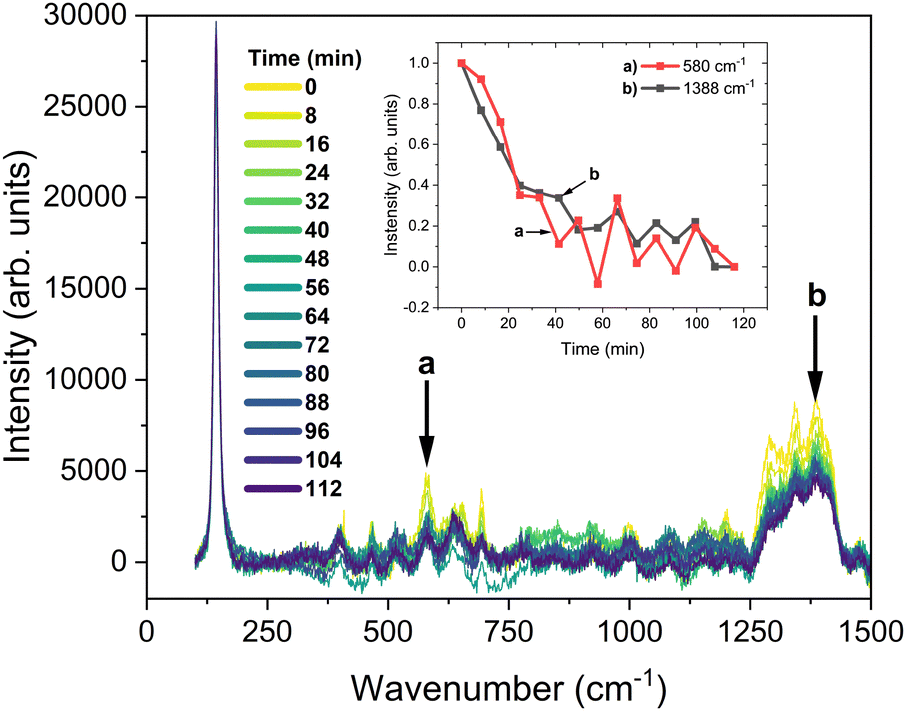 | ||
| Fig. 2 Time-dependent Raman spectra at probed temperature and corresponding vibrations of acetonitrile. Spectra have been baseline-subtracted and normalized by the main peak of TiO2. | ||
Time-dependent in situ Raman measurements provided insights into the solid-state formation process. For the data shown in Fig. 2 and Fig. S13 (ESI†), an assembled solar cell was subjected to a controlled heating profile: the temperature was ramped from ambient to 70 °C at a rate of 30 °C min−1, and then maintained at 70 °C for 70 minutes. The spectra in Fig. 2 were acquired sequentially during this 70 minutes isothermal period from a cell that had previously undergone one identical full heat treatment cycle. This allowed observation of the later stages of solvent evaporation and HTM consolidation. The process can be tracked via characteristic acetonitrile peaks, notably the δ(C–CN) mode at 580 cm−1, which diminished by over 95% within the first 60 minutes of this hold (Fig. S14, ESI† and inset of Fig. 2), and δ(C–H) modes between 1250–1450 cm−1, indicating effective solvent removal under these conditions.
The choice of Lewis base additive, such as 4-tert-butylpyridine (tBP) or N-methylbenzimidazole (NMBI), significantly influences the properties of the liquid electrolyte and the subsequent solid-state formation process, thereby impacting device performance.22,27 While NMBI-containing liquid electrolytes yielded comparable or slightly higher initial efficiencies compared to tBP-containing devices, once solidified they often exhibited a more pronounced decrease in performance and higher variability post-solidification (see Tables S4 and S5, ESI† for 2-week data). This behavior is often attributed in literature to the higher propensity of NMBI to crystallize within the HTM upon solvent removal, which can disrupt the HTM morphology and compromise interfacial contacts.28 In contrast, tBP appeared to promote a more stable and morphologically favorable HTM layer under our accelerated solidification conditions, as suggested by the SEM image in Fig. 3 (showing a compact, amorphous-like HTM with tBP) and the generally better performance and reproducibility observed in the solid state. To further probe the interfacial electronic differences resulting from the choice of base, photoinduced absorption (PIA) spectra were compared for devices solidified (70 °C for 20 minutes) using either NMBI or tBP as additives. The PIA spectra (ESI,† Fig. S11) for tBP-containing devices exhibit features more consistent with efficient dye regeneration and favorable interfacial charge transfer kinetics (e.g., deeper ground-state bleach (GSB, vide infra), better quenching of oxidized dye peak) compared to NMBI-containing cells processed under identical conditions. This photophysical evidence, while indirect regarding crystallinity, supports the observed superior performance of tBP in solid-state devices formed via our rapid thermal protocol and underscores its role in facilitating a well-functioning TiO2/dye/HTM interface, likely by mitigating detrimental morphological changes such as extensive crystallization during solidification.
 | ||
| Fig. 3 Cross-sectional SEM image at 2500× magnification of a solid-state DSC after the solid-state formation process at 70 °C. | ||
SEM was used to gain further insight into the morphology of the interface between the photoactive layer and the HTM (Fig. 3). A clear aggregation of the over-standing HTM layer (6 μm) on top of the mTiO2 layer (4 + 4 μm) could be observed. An amorphous HTM supports fast dye regeneration, high efficiency, and optimal contact with the PEDOT counter electrode and absorbed dye molecules from the DSCs fabricated with this method.1 The amorphous bulk structure of the HTM reduces electron recombination at grain boundaries and results in fast regeneration kinetics as it will be discussed later (Fig. 4 and 5). Improved photocurrent densities under low-light conditions (from 71 to 79 μA cm−2 under 1000 lux illumination, Table 1) are a result of the increased charge transfer mobility of the solid HTM, whereas limitations of the photocurrent at higher light intensities are due to the larger electron density that is trapped in the oxidized dye.29,30
 | ||
| Fig. 4 Electron lifetime (left) and charge transport time (right) before (solid line) and after (dotted line) the solid-state formation process at 70 °C. | ||
| # | 1 sun 70 °C | V OC (mV) | J SC (mA cm−1) | FFc (%) | PCEd (%) |
|---|---|---|---|---|---|
| a Open-circuit voltage. b Short-circuit current density. c Fill factor. d Power conversion efficiency. e 5% discarded samples. f 40% discarded samples. g 60% discarded samples. | |||||
| I | Liquid EL | 1040 | 12.27 | 75.8 | 9.68 |
| II | 2 min | 1028 | 11.87 | 75.3 | 9.20 |
| III | 10 min | 1025 | 10.45 | 74.0 | 8.02e |
| IV | 20 min | 1000 | 9.03 | 71.9 | 6.79e |
| V | 30 min | 1006 | 10.38 | 73.8 | 7.77f |
| VI | 60 min | 995 | 5.96 | 76.6 | 4.44g |
Additionally, SEM images of photovoltaic devices implementing only the mTiO2 layer, the mTiO2 and the copper complex in solution, and the mTiO2 and a drop-casted HTM were recorded (Fig. S2–S5, ESI†). These samples were characterized using energy-dispersive X-ray spectroscopy (EDX, Fig. S6, ESI†) to monitor impurities and changes in the elemental composition of the interface after electrolyte interaction, especially after formation of the solid-state HTM. The EDX analysis of the solidified copper electrolyte with solid-state formation condition IV showed copper contents of over 0.3%, being consistent with the literature and liquid-junction DSCs.1 Thus, EDX not only supports sufficient pore infiltration and regeneration of the oxidized dye molecules (Fig. 5(b)) but also provides a method to monitor any residual elements left after electrolyte evaporation and cell operation.23,31 Studies utilizing drop casting of the electrolyte with a subsequent temperature-induced solid-state formation process showed improvements in the performance of DSCs in combination with polyiodides.2 In contrast, in combination with copper coordination complexes, as the investigated Cu(I/II)(tmby)2, led to crystallization on the mTiO2 surface (Fig. S7, ESI†). This highlights the need for alternative solid-state formation processes.
 | ||
| Fig. 5 (a) Transient absorption spectroscopy. (b) Baseline-corrected photoinduced absorption spectra for devices with liquid electrolyte and solid HTMs formed at 70 °C for different durations. Features include the dye's ground-state bleach (∼630 nm) and oxidation (650–850 nm). Raw spectra are provided in Fig. S10 (ESI†). | ||
Electron lifetime and charge transfer measurements before and after the solid-state formation process at 70 °C are displayed in Fig. 4. In agreement with performance measures (Table 1), similar electron lifetimes can be observed for liquid-junction cells and devices with a solid-state formation process at 70 °C up to 20 minutes, while reduced lifetimes occur for heat treatments above 30 minutes. A similar trend is found for transport times. The increase in photocurrent under indoor illumination stems from increasing effects of electronic conduction of the hole hopping mechanism,1,32 compared to the slower charge transfer via ionic diffusion and migration in the liquid electrolyte,33,34 and it supports the aforementioned successful solid-state formation of the liquid electrolyte.
Charge collection properties were characterized with incident-photon-to-electron conversion efficiency measurements, which followed the overall trend (Fig. S8, ESI†). Even a brief heat treatment at 70 °C for 20 minutes led to a 5% reduction in conversion efficiency, supporting the aforementioned decrease in electron lifetime and photocurrent density under solar irradiation in Table 1, but showing opposite trends to the increase in current density for this set of experiments under ambient conditions. The elevated current densities under low-light conditions can be explained via the improved charge transfer kinetics (Fig. 4) and a reduced space charge formation.30,35 Longer heat exposures are reported to reduce electron diffusion lengths,36 which is indicated by the narrowing of the IPCE spectra at elevated temperatures (Fig. S8, ESI†). Therefore, improvements in the photovoltaic performance are due to improved photocurrent densities observed for short solid-state formation times, while excessive heat exposure negatively affects the performance. PCEs increase to a maximum value of 15.59% (+1.45%, condition III) for only partly-dried devices after 10 minutes (Table 1), and retain a gain compared to the liquid state also for fully-dried HTM after 20 minutes (+0.57%, condition IV).
Characterization of the transient oxidized dye species provided pivotal information about the dye regeneration effectivity of the HTM. TAS measurements on cells comprising an inert electrolyte, a liquid electrolyte, or a solid HTM are displayed in Fig. 5(a) and Fig. S12 (ESI†). Lifetimes of the transient species in the nanosecond region can be observed for the liquid electrolyte as well as for a short temperature treatment of 20 minutes (70 °C), with lifetimes of 575 ± 140 ns and 487 ± 150 ns, respectively. Considerably longer lifetimes of 26.8 μs and 62.0 μs are observed, respectively, for solid-state formation over 60 minutes at 70 °C and the inert electrolyte (in the absence of the redox couple). Electron lifetimes and transport times in Fig. 4 are in the order of ms, considerably longer than the lifetimes of the transient species of the oxidized dye (ns) in DSCs with the HTMs after short solid-state formation times. Slower regeneration of the oxidized dye (μs) in longer solid-state formation processes of 60 minutes in Fig. 5 resulted in increased charge recombination, leading to low photovoltages and photocurrents (Table 1).
The regeneration efficiency of the oxidized dye can be calculated according to eqn (1),15,37 resulting in near-unity regeneration (99.2%) for short solid-state formation times and lower regeneration efficiencies (56.8%) at elevated temperatures of 70 °C for 60 minutes.
 | (1) |
Photoinduced absorption spectroscopy (PIA) offered further insights into dye regeneration and interfacial electrostatics. Representative PIA spectra, baseline-corrected for clarity (see Fig. S10, ESI† for raw data), are shown in Fig. 5(b). A distinct negative feature around 630 nm, corresponding to the GSB of the Y123 sensitizer (confirming its efficient photoexcitation), was attributed to the Stark effect. This electrochromic shift of the dye's ground-state absorption spectrum is induced by the local electric field generated by photoinjected electrons in the TiO2 and oxidized HTM species.38 The magnitude and shape of these Stark features are sensitive to the local electric field strength and charge distribution. Efficient dye regeneration by the Cu(I) species in the HTM resulted in the quenching of the photo-oxidized dye (Y123+) absorption, which typically appears as a positive signal at longer wavelengths (>650 nm). In the liquid electrolyte and for HTMs after short heat treatments (0 °C for up to 20 minutes), the pronounced GSB signals, along with effective Y123+ quenching (inferred from the overall spectral evolution and comparison with inert electrolyte TAS, Fig. 5(a)), indicated efficient primary charge separation and subsequent dye regeneration. Conversely, changes in PIA spectral shape upon prolonged heat treatment, such as diminished GSB signals or less effective Y123+ quenching, would suggest impaired regeneration or increased recombination.
Electrochemical impedance spectroscopy (EIS) was employed to investigate interfacial charge transfer kinetics. All measurements on assembled cells were conducted under 1 sun illumination (100 mW cm−2, AM1.5G simulated) or in the dark at the open circuit potential (VOC). Representative Nyquist plots for different conditions are shown in Fig. S16 and S19 (ESI†). The impedance spectra were fitted using the equivalent circuit model depicted in Fig. S15 (ESI†), which typically comprises a series resistance (Rs), a high-frequency element corresponding to the TiO2/dye/HTM interface of the mesoporous electrode (DX11, Bisquert #2 element (transmission line model) in ZView), and a medium/low-frequency R-CPE element associated with the counter electrode/HTM interface (RCT,CE, CPECE). For liquid electrolytes, a Warburg diffusion element (Ws) is also included. Under illumination, for the fresh liquid electrolyte, RCT,TiO2 was determined to be approximately 5 Ω. Following solid-state formation (after 20 minutes of heat treatment at 70 °C), RCT,TiO2 remained low at approximately 4 Ω, indicating that efficient charge transfer pathways at the TiO2/dye/HTM interface are maintained. The charge transfer resistance at the counter electrode interface (RCT,CE) also remained similar for the two cases, with approximate values of 20 Ω and 10 Ω, respectively, for the liquid and solid-state (20 min, 70 °C) cases. For longer heating process times (60 min, 70 °C), however, the RCT, TiO2 became very large (approximately 310 kΩ), dominating the spectrum and shadowing all other parameters. This is consistent with increased charge recombination and the observed decrease in overall device performance (Table 1).
The results of the current/voltage scans under 100 mW cm−2 solar radiation and 1000 lux, 4000 K LED lamp conditions are summarized in Table 1. The performance metrics of each temperature are tracked for the initial copper coordination complex in solution, and subsequently for solid-state formation times of 2, 10, 20, 30 and 60 minutes at 70 °C. All tests were following repeatable conditions. Primary results under 100 mW cm−2 solar radiation showed an overall decrease in the performance of the ssDSCs, mainly attributed to a decrease in the photocurrent density of the dried cells.
In addition to the optimal 70 °C thermal process, other processing temperatures were tested. The solid-state formation process at 50 °C led to a decrease to 95% of the initial efficiency after 60 minutes exposure (Table S1, ESI†), however devices were visually not fully dried. Moving to temperatures higher than the boiling point of acetonitrile (82 °C), a process temperature of 90 °C led to an almost instantaneous decrease in the photovoltaic performance, with performances below 8% after 2 minutes and fully failing devices after 10 minutes (Table S2, ESI†). The crystallization of the HTM is the main reason for the performance-related decreases, owing to reduced contact with the absorbed dye and counter electrode, and the formation of grain boundaries (Fig. 1 and Fig. S7, ESI†). An even higher processing temperature of 110 °C led to a too quick evaporation of acetonitrile, which disrupted the formation of the HTM layer, leading to fully failing devices already after 2 minutes (Table S3, ESI†). Electron lifetime and transport time, PIA, and EIS measurements for these processing temperatures can be found in Fig. S9, S10 and S16–S18 (ESI†), respectively. Efforts to further accelerate the solid-state formation of the HTM involved processing under reduced pressure at 50 °C, which resulted in an increased defect rate of the devices and overall decreased efficiencies (Table S6, ESI†) compared to the optimal processing conditions.
Promising results were achieved under ambient light conditions. A stable cell photovoltage over 830 mV, and an increase in photocurrent density up to 74 μA cm−2 under 1000 lux illumination were achieved after the initial solid-state formation process at 70 °C for 20 minutes. This resulted in a stable ssDSC performance of 14.7% for the Cu(tmby)2 coordination complexes in conjunction with the organic Y123 sensitizer.
4 Conclusions
In conclusion, this study provided useful insights and characterization for the transitioning of liquid electrolytes to solid HTMs. The accelerated solid-state formation was tracked via time-dependent Raman spectra at elevated temperatures and showed near-unity solid-state formation of the HTM. Increased, stable photocurrent density (+3.03 μA cm−2) and photovoltaic performance (+0.57%) under low-light conditions for a short heat exposure were attributed to improved charge transfer kinetics and reduced space charge formation. Fast regeneration kinetics of the solid HTM were quantified through transient species measurements and impedance spectroscopy. The accelerated solid-state formation process at 70 °C for 20 minutes showed the best photovoltaic performance while ensuring the formation of the HTM. The data highlighted the importance of controlling the morphology in the bulk material through solid-state formation conditions to achieve high-performance ssDSCs. In addition, this study provides a guideline towards the assessment of reproducible solid-state HTM formation in metal complex-based DSCs and highlights the challenges and difficulties in the successful transition from liquid electrolytes into solid HTMs.The development of a rapid and reproducible solidification protocol also holds considerable promise for enhancing the scalability of ssDSC fabrication. While the present study focused on small area lab-scale devices, the principles of controlled thermal processing are fundamentally adaptable to larger areas. Previous work utilizing solvent evaporation for HTM formation in DSCs, including studies from our group with Cu complexes (albeit with slower drying for larger devices intended for IoT applications)18 and by others for different HTM systems on device areas up to 15.7 cm2,2 indicates the general feasibility of such approaches for fabricating mini-modules. Our accelerated solidification method offers a distinct advantage by drastically reducing the overall processing time, a critical factor for achieving higher throughput. For potential translation to continuous manufacturing techniques, such as roll-to-roll processing on flexible substrates, this rapid thermal step is significantly more compatible with typical industrial line speeds than multi-day drying cycles. Key engineering challenges would involve ensuring highly uniform heat distribution across the substrate width, designing efficient solvent vapor extraction systems to maintain consistent solidification kinetics, and optimizing large-area electrolyte deposition techniques (e.g., slot-die coating or printing) to manage solvent egress from potentially porous electrode structures prior to final device sealing. Further optimization of electrode architecture, perhaps incorporating features to facilitate uniform solvent removal from larger areas, may also be beneficial. Regarding the practical implications and long-term stability of devices fabricated using this accelerated solidification protocol, it is pertinent to note the robust durability previously demonstrated for Cu complex-based “Zombie” ssDSCs. Seminal studies by Freitag, Cao et al.1,5,18 and Zhang et al.4 have shown that well-encapsulated devices can retain high performance for over 1000 hours under ambient storage or continuous light soaking. Furthermore, our group has previously demonstrated the operational stability of such ssDSCs when powering IoT devices under intermittent ambient light over extended periods, showcasing their suitability for real-world applications.18 Recent work by Santos et al. also highlights the stability of solid-state Cu complex HTM devices in a monolithic architecture.39 The achievement of a rapid and reproducible method that promotes a favorable amorphous HTM morphology is expected to be conducive to good long-term stability. This work provides a critical step towards standardized fabrication, which is essential for future systematic investigations into the operational and shelf-life stability crucial for bridging the gap towards commercial viability.
Future research should focus on the molecular engineering of asymmetric and heteroleptic copper coordination complexes, where fundamental physical chemistry principles offer compelling advantages beyond the already-optimized dye regeneration efficiency (99%). While symmetric Cu(tmby)2 complexes demonstrate excellent regeneration kinetics, their tendency to crystallize at elevated temperatures (>90 °C) creates grain boundaries that impede charge transport and increase interfacial resistance. Asymmetric complexes, through their inherent structural irregularity, could disrupt molecular packing and maintain an amorphous state during solid-state formation, thereby minimizing grain boundary formation and enhancing charge carrier mobility.40 The introduction of different coordination environments in heteroleptic complexes could also enable precise control over the Cu(I/II) reorganization energy – a critical parameter that influences charge transfer rates at interfaces beyond the initial dye regeneration step.41,42 These molecular design strategies,21 combined with our optimized thermal processing protocol (70 °C, 20–70 min), provide a clear pathway toward next-generation solid-state hole transport materials where interface engineering and morphological control, rather than regeneration kinetics, become the key determinants of device performance.
Conflicts of interest
There are no conflicts to declare.Data availability
The experimental data supporting the findings of this study are available in the ESI,† including detailed photovoltaic performance metrics, SEM and microscopy images, EDX analysis, spectroscopic measurements (IPCE, PIA, TAS, time-resolved Raman), and electrochemical impedance spectroscopy data. Raw data files for all characterization measurements are available from the corresponding author upon reasonable request. The femtosecond TAS measurements data used in this work is stored in Newcastle University's data repository. Additional experimental details and characterization data are included in the ESI.†Acknowledgements
The authors wish to thank Michael Grätzel and Felix Eickemeyer (EPFL – Swiss Federal Institute of Lausanne) for their insightful discussions and valuable inputs during this project. We also extend our thanks to Dr Owen Woodford (Newcastle University) for acquiring the femtosecond transient absorption spectroscopy measurements used in this work, and to Isabel Arce-Garcia (Newcastle University) for her technical support. MF acknowledges financial support from UK Research and Innovation through the Engineering and Physical Sciences Research Council (EPSRC) under grants EP/W006340/1 (North East Ultrafast Transient Absorption Spectroscopy Facility) and EP/V035819/1 (Photocapacitors for Ambient Energy Applications). Additionally, we gratefully acknowledge The Royal Society for supporting this work via University Research Fellowships, under grants IES/R3/213090, RF/ERE/210025, and URF/R1/191286. This work was further supported by EPSRC (grant number EP/S023836/1). IB acknowledges support from Project CH4.0 under the MUR program “Dipartimenti di Eccellenza 2023–2027” (CUP: D13C22003520001), and from the PNA4Energy project, funded under the MUR program “PNNR M4C2 Initiative 1.2: Young Researcher – Seal of Excellence” (CUP: D18H22001950007).Notes and references
- Y. Cao, Y. Saygili, A. Ummadisingu, J. Teuscher, J. Luo, N. Pellet, F. Giordano, S. M. Zakeeruddin, J. E. Moser, M. Freitag, A. Hagfeldt and M. Grätzel, Nat. Commun., 2017, 8, 15390 CrossRef PubMed.
- M. Sutton, B. Lei, H. Michaels, M. Freitag and N. Robertson, ACS Appl. Mater. Interfaces, 2022, 14, 43456–43462 CrossRef CAS.
- Y. Saygili, M. Stojanovic, H. S. Kim, J. Teuscher, R. Scopelliti, M. Freitag, S. M. Zakeeruddin, J. E. Moser, M. Grätzel and A. Hagfeldt, J. Phys. Chem. C, 2020, 124, 7071–7081 CrossRef CAS.
- W. Zhang, Y. Wu, H. W. Bahng, Y. Cao, C. Yi, Y. Saygili, J. Luo, Y. Liu, L. Kavan, J.-E. Moser, A. Hagfeldt, H. Tian, S. M. Zakeeruddin, W.-H. Zhu and M. Grätzel, Energy Environ. Sci., 2018, 11, 1779–1787 RSC.
- M. Freitag, Q. Daniel, M. Pazoki, K. Sveinbjörnsson, J. Zhang, L. Sun, A. Hagfeldt and G. Boschloo, Energy Environ. Sci., 2015, 8, 2634–2637 RSC.
- E. Tanaka and N. Robertson, J. Mater. Chem. A, 2020, 8, 19991–19999 RSC.
- C. T. Weisspfennig, D. J. Hollman, C. Menelaou, S. D. Stranks, H. J. Joyce, M. B. Johnston, H. J. Snaith and L. M. Herz, Adv. Funct. Mater., 2014, 24, 668–677 CrossRef CAS.
- W. Cho, J. Lim, T.-Y. Kim, Y. R. Kim, D. Song, T. Park, F. Fabregat-Santiago, J. Bisquert and Y. S. Kang, J. Phys. Chem. C, 2016, 120, 2494–2500 CrossRef CAS.
- J. Lu, Y.-C. Chang, H.-Y. Cheng, H.-P. Wu, Y. Cheng, M. Wang and E. W.-G. Diau, ChemSusChem, 2015, 8, 2529–2536 CrossRef CAS PubMed.
- C. T. Weisspfennig, M. M. Lee, J. Teuscher, P. Docampo, S. D. Stranks, H. J. Joyce, H. Bergmann, I. Bruder, D. V. Kondratuk, M. B. Johnston, H. J. Snaith and L. M. Herz, J. Phys. Chem. C, 2013, 117, 19850–19858 CrossRef CAS.
- S. K. Yadav, S. Ravishankar, S. Pescetelli, A. Agresti, F. Fabregat-Santiago and A. Di Carlo, Phys. Chem. Chem. Phys., 2017, 19, 22546–22554 RSC.
- K. Zeng, Y. Chen, W. H. Zhu, H. Tian and Y. Xie, J. Am. Chem. Soc., 2020, 142, 5154–5161 CrossRef CAS PubMed.
- Y. Saygili, M. Söderberg, N. Pellet, F. Giordano, Y. Cao, A. B. Munoz-García, S. M. Zakeeruddin, N. Vlachopoulos, M. Pavone, G. Boschloo, L. Kavan, J. E. Moser, M. Grätzel, A. Hagfeldt and M. Freitag, J. Am. Chem. Soc., 2016, 138, 15087–15096 CrossRef CAS PubMed.
- M. Freitag, F. Giordano, W. Yang, M. Pazoki, Y. Hao, B. Zietz, M. Grätzel, A. Hagfeldt and G. Boschloo, J. Phys. Chem. C, 2016, 120, 9595–9603 CrossRef CAS.
- E. Tanaka, H. Michaels, M. Freitag and N. Robertson, J. Mater. Chem. A, 2020, 8, 1279–1287 RSC.
- B. O'Regan and M. Grätzel, Nature, 1991, 353, 737–740 CrossRef.
- Y. Ren, D. Zhang, J. Suo, Y. Cao, F. T. Eickemeyer, N. Vlachopoulos, S. M. Zakeeruddin, A. Hagfeldt and M. Grätzel, Nature, 2023, 613, 60–65 CrossRef CAS.
- H. Michaels, M. Rinderle, R. Freitag, I. Benesperi, T. Edvinsson, R. Socher, A. Gagliardi and M. Freitag, Chem. Sci., 2020, 11, 2895–2906 RSC.
- D. Zhang, M. Stojanovic, Y. Ren, Y. Cao, F. T. Eickemeyer, E. Socie, N. Vlachopoulos, J. E. Moser, S. M. Zakeeruddin, A. Hagfeldt and M. Grätzel, Nat. Commun., 2021, 12, 1777 CrossRef CAS PubMed.
- H. Michaels, M. Rinderle, I. Benesperi, R. Freitag, A. Gagliardi and M. Freitag, Chem. Sci., 2023, 14, 5350–5360 RSC.
- S. M. Meethal, S. C. Pradhan, J. Velore, S. Varughese, R. S. Pillai, F. Sauvage, A. Hagfeldt and S. Soman, J. Mater. Chem. A, 2024, 12, 1081–1093 RSC.
- Y. Saygili, M. Stojanovic, H. Michaels, J. Tiepelt, J. Teuscher, A. Massaro, M. Pavone, F. Giordano, S. M. Zakeeruddin, G. Boschloo, J. E. Moser, M. Grätzel, A. B. Muñoz-García, A. Hagfeldt and M. Freitag, ACS Appl. Energy Mater., 2018, 4950–4962 CrossRef CAS.
- Y. Cao, Y. Liu, S. M. Zakeeruddin, A. Hagfeldt and M. Grätzel, Joule, 2018, 2, 1108–1117 CrossRef CAS.
- V. Majer, V. Svoboda and H. V. H. V. Kehiaian, Enthalpies of vaporization of organic compounds: a critical review and data compilation, Blackwell Scientific Publications, Oxford [Oxfordshire]; Boston, England, United Kingdom, 1985 Search PubMed.
- K. B. Ørnsø, E. O. Jónsson, K. W. Jacobsen and K. S. Thygesen, J. Phys. Chem. C, 2015, 119, 12792–12800 CrossRef.
- V. Vaissier, P. Barnes, J. Kirkpatrick and J. Nelson, Phys. Chem. Chem. Phys., 2013, 15, 4804–4814 RSC.
- S. O. Fürer, R. A. Milhuisen, M. K. Kashif, S. R. Raga, S. S. Acharya, C. Forsyth, M. Liu, L. Frazer, N. W. Duffy, C. A. Ohlin, A. M. Funston, Y. Tachibana and U. Bach, Adv. Energy Mater., 2020, 10, 2002067 CrossRef.
- F. Lamberti, T. Gatti, E. Cescon, R. Sorrentino, A. Rizzo, E. Menna, G. Meneghesso, M. Meneghetti, A. Petrozza and L. Franco, Chem, 2019, 5, 1806–1817 CAS.
- H. J. Snaith, A. Petrozza, S. Ito, H. Miura and M. Grätzel, Adv. Funct. Mater., 2009, 19, 1810–1818 CrossRef CAS.
- S. Beuel, P. Hartnagel and T. Kirchartz, Adv. Theory Simul., 2021, 4, 2000319 CrossRef CAS.
- K. Zouhri, M. Spencer, K. Nulph, P. Appiah-Kubi and K. A. Shiral Fernando, Sol. Energy, 2022, 241, 343–360 CrossRef CAS.
- U. Bach, D. Lupo, P. Comte, J. E. Moser, F. Weissörtel, J. Salbeck, H. Spreitzer and M. Grätzel, Nature, 1998, 395, 583–585 CrossRef CAS.
- M. Wang, C. Grätzel, S. M. Zakeeruddin and M. Grätzel, Energy Environ. Sci., 2012, 5, 9394–9405 RSC.
- J. Wu, Z. Lan, J. Lin, M. Huang, Y. Huang, L. Fan and G. Luo, Chem. Rev., 2015, 115, 2136–2173 CrossRef CAS PubMed.
- K. Schwarzburg and F. Willig, J. Phys. Chem. B, 2003, 107, 3552–3555 CrossRef CAS.
- P. Wang, L. Yang, H. Wu, Y. Cao, J. Zhang, N. Xu, S. Chen, J.-D. Decoppet, S. M. Zakeeruddin and M. Grätzel, Joule, 2018, 2, 2145–2153 CrossRef CAS.
- H. Michaels, I. Benesperi, T. Edvinsson, A. B. Muñoz-Garcia, M. Pavone, G. Boschloo and M. Freitag, Inorganics, 2018, 6, 53 CrossRef.
- U. B. Cappel, S. M. Feldt, J. Schöneboom, A. Hagfeldt and G. Boschloo, J. Am. Chem. Soc., 2010, 132, 9096–9101 CrossRef CAS.
- F. Santos, D. Ivanou and A. Mendes, Sol. RRL, 2024, 8, 2300574 CrossRef CAS.
- C. E. Housecroft and E. C. Constable, Chem. Sci., 2022, 13, 1225–1262 RSC.
- A. Lennert and D. M. Guldi, ChemPhotoChem, 2019, 3, 636–644 CrossRef CAS.
- H. Rui, J. Shen, Z. Yu, L. Li, H. Han and L. Sun, Angew. Chem., Int. Ed., 2021, 60, 16156–16163 CrossRef CAS PubMed.
Footnote |
| † Electronic supplementary information (ESI) available. See DOI: https://doi.org/10.1039/d5cp01292a |
| This journal is © the Owner Societies 2025 |