
 Open Access Article
 This Open Access Article is licensed under a Creative Commons Attribution-Non Commercial 3.0 Unported Licence
Ionic conductivity of vanadium-doped tin disulfide for photovoltaic applications†
Shafi
Ullah
a,
Hanif
Ullah
b,
Abel
García-Bernabé
c,
Andreu
Andrio
 d,
Bernabe Mari
Soucase
a and
Vicente
Compañ
*c
d,
Bernabe Mari
Soucase
a and
Vicente
Compañ
*c
aInstituto de diseño y Fabricación (IDF)-Universitat Politècnica de València (UPV), Camino de Vera, s/n, 46022 Valencia, Spain
bDepartment of Electrical Engineering, Federal Urdu University (FUUAST) Islamabad, Pakistan
cDepartamento de Termodinámica Aplicada (ETSII), Universitat Politècnica de València, Camino de Vera s/n, 46022 Valencia, Spain. E-mail: vicommo@ter.upv.es
dDepartamento de Física, Universitat Jaume I, 12071. Castellón de la Plana, Spain
First published on 13th June 2025
Abstract
Tin disulfide (SnS2) is an environmentally friendly and widely available material with a band gap ranging from approximately 2.20 to 2.45 eV, making it a strong candidate for use as a buffer layer in photovoltaic technologies. In this study, SnS2 was synthesized using the hydrothermal method. To enhance its interaction with visible light, vanadium (V) atoms—also earth-abundant and characterized by a low band gap—were incorporated into the SnS2 matrix. The atomic percentage of vanadium was varied from 0% to 10% in increments of 2%. A previous study conducted on similar mixed Sn1−xVxS2 samples, though with different vanadium concentrations, suggested that V-doped SnS2 thin films could be suitable as buffer layers for solar cell fabrication. However, the electrical conductivity of these samples had not been quantified, and therefore, such a conclusion cannot be definitively confirmed. In this work, electrochemical impedance spectroscopy was used to determine the conductivity and diffusivity of vanadium-doped samples as a function of temperature. Our results revealed a percolation threshold at approximately 6% vanadium content, with notable changes in conductivity observed around 120 °C. The sample doped with 6% vanadium exhibited a significantly enhanced photocurrent response (3.0 × 10⁻⁶ A cm−2) compared to the undoped SnS2 thin films (4.0 × 10⁻⁷ A cm−2). These findings indicate that vanadium incorporation significantly alters the crystallinity of SnS2, leading to changes in the melting temperature of the mixed Sn1−xVxS2 samples. Such changes may induce structural relaxation, lattice dilation, or enhanced atomic interactions. Together with previous studies, these results highlight that V-doped SnS2 is a promising candidate for optoelectronic applications, including photoelectrochemical catalysis, photodetectors, and photovoltaic devices.
1. Introduction
In recent years, binary, ternary, and quaternary compound semiconductors have demonstrated significant potential for optoelectronic applications.1 Among these, materials such as ternary chalcogenides (e.g., CuGaS2), quaternary chalcogenides (e.g., CuInGaSe2 or CIGSe2), and binary chalcogenides (e.g., CdTe) have shown considerable promise for large-scale photovoltaic applications. However, their commercial deployment faces several challenges, including high production costs, the toxicity of selenium (Se), and the limited availability of critical elements such as indium (In), tellurium (Te), and gallium (Ga). Additional concerns include difficulties in achieving precise stoichiometry and high purity, mechanical instability, and overall high material and processing expenses. These limitations have significantly hindered the widespread commercialization of these materials.2 Despite these challenges, binary CdS-based thin-film solar cells—such as CdTe/CdS—have successfully addressed some of these limitations due to their relatively simple stoichiometric control and improved photoconversion efficiency. Moreover, cadmium sulfide (CdS), an n-type semiconductor with a band gap of approximately 2.45 eV, has been extensively studied and widely used as a window layer in various optoelectronic devices.3 To overcome the limitations associated with CdS, we propose the use of SnS2 as an alternative. SnS2 offers superior optical and structural properties, making it a promising substitute for CdS in photovoltaic and other optoelectronic applications.4SnS and SnS2 are simple binary compounds that are abundant, non-toxic, and widely available on Earth. These materials offer easily controllable stoichiometry and are environmentally friendly. They exhibit favorable optoelectronic and electrical properties, making them suitable for use in thin-film solar cells. Specifically, SnS is a promising absorber material, known for its high carrier mobility and p-type electrical conductivity. According to the literature, SnS thin films exhibit a direct optical band gap ranging from 1.2 to 1.5 eV, with an indirect optical transition between 1.0 and 1.2 eV.5 Nevertheless, the reported conversion efficiency of SnS-based devices is around 4.4%, which is significantly lower than its theoretical efficiency of approximately 33%. This discrepancy is likely attributed to band gap misalignment between the absorber and buffer layer interface.6 To address this issue, the use of SnS2 as a buffer layer is proposed. The polycrystalline quality, non-toxicity, abundance of SnS2, and high absorption coefficient (>104 cm−1) make it a promising candidate. Furthermore, its energy band gap, ranging from 0.8 to 2.88 eV, along with its n-type conductivity, enhances its suitability as a buffer layer for photovoltaic applications.7
Numerous studies have explored various techniques for preparing SnS2 buffer layers, including vacuum evaporation, solvothermal methods, reactive evaporation, chemical vapor deposition (CVD), physical vapor deposition (PVD), and molecular beam epitaxy (MBE).8 Additionally, chemical spray pyrolysis, along with methods such as vacuum evaporation and solvothermal techniques, has been employed.9–11 However, these methods are primarily based on high-cost vacuum processes, which significantly increase production expenses. Despite this, there are relatively few studies focusing on the synthesis of SnS2 thin films using the more cost-effective hydrothermal method for photovoltaic applications. In our previous studies, we observed improvements in the optical and conductivity properties of SnS2 doped with chromium (Sn1−xCrxS2). Samples prepared using the low-cost hydrothermal technique demonstrated that Sn1−xCrxS2 powders with x = 6% exhibited a lower optical bandgap energy compared to pure SnS2 samples.12 Additionally, the conductivity measured along the plane between 80 °C and 100 °C was approximately 5 × 10⁻⁴ S cm−1. We observed that doping SnS2 thin films with chromium resulted in the effective substitution of Sn atoms with Cr atoms within the SnS2 framework. This substitution not only reduced the lattice size and allowed for tunable interlayer spacing but also modified the electrical properties, primarily due to the smaller atomic radius of Cr compared to Sn.
In this study, we investigated the effect of vanadium (V) doping on the formation of SnS2 using an inexpensive, simple, and vacuum-free hydrothermal technique. This method has the potential to significantly reduce the fabrication costs of photovoltaic devices by minimizing the mismatch between the absorber and window layers, which is typically caused by the formation of CdS. To achieve this, SnS2 doped with varying amounts of vanadium (Sn1−xVxS2), with molar ratios of x = 0, 2, 4, 6, 8, and 10%, were synthesized and characterized. Previous studies, including X-ray diffraction (XRD), scanning electron microscopy (SEM), optical absorption and transmission, and elemental electrochemical analysis, were carried out to assess the material properties.13 The results revealed that the incorporation of vanadium (V) affects the morphology, with V content being uniformly dispersed over the surface. Furthermore, optical analysis demonstrated that after the incorporation of V, the film's transmission decreased, while absorption increased. This led to a gradual reduction in the band gap, shifting to lower energy wavelengths. The photoelectrochemical analysis showed that the vanadium-doped SnS2 exhibited a photocurrent of 2.89 μA cm−2, compared to the undoped SnS2. Our results demonstrate that vanadium content plays a significant role when incorporated into the SnS2 compound, making it a promising candidate for optoelectronic applications such as photoelectrochemical catalysts, photodetectors, and particularly for photovoltaic applications. However, to gain a deeper understanding of these effects, it is essential to quantify the conductivity and diffusivity of charge carriers in the Sn1−xVxS2 samples as a function of vanadium concentration. Therefore, in this paper, we conducted a study to determine the electrical conductivity and ionic diffusivity using electrochemical impedance spectroscopy (EIS) measurements. These characteristics are crucial for assessing the commercial potential of this simple and cost-effective synthesis method. By examining the conductivity and durability of Sn1−xVxS2 powders, we aim to evaluate their suitability and reliability for various practical applications. To achieve this, we measured the through-plane conductivity of the doped SnS2 powders using electrochemical impedance spectroscopy (EIS) to quantify their transverse conductivity. This approach builds upon the research methodology we previously employed for polyelectrolytes.14,15 In this study, we applied the Coelho model and incorporated the electrode polarization (EP) method, represented by a Debye relaxation, for the characterization of the complex dielectric permittivity ε*,15–17 where the imaginary part of the permittivity was fitted (ε′′). The experimental data obtained for each of the samples studied allow us to determine the diffusivity, mobility, and charge carrier density of the different samples. These parameters provide insights into the cumulative processes occurring within the system, including the interactions between charge carriers and the mobile ion concentration of vanadium in the doped SnS2. Conductivity measurements will offer valuable information on the behavior of the samples and their potential suitability as a buffer layer for photovoltaic applications.
2. Experimental detail
All starting materials were used as received without further purification. A 0.005 M solution of SnCl4·5H2O was prepared in 20 mL of water, with tartaric acid (C4H6O6) dissolved in the same solution to serve as the tin source. For the sulfur source, a 0.02 M solution of thioacetamide (CH3–CS–NH2) was prepared using the same procedure as for the tin solution. Both solutions were combined and stirred for 30 minutes. The resulting mixture was then transferred to a 50 mL Teflon-lined stainless-steel autoclave, which was placed in an electric oven and heated at 200 °C for 12 hours, as described in our previous work.18 After the reaction, the product was cleaned with water and ethanol by centrifugation at 4000 rpm, and the final product was dried at 100 °C for 5 hours. Samples of SnS2 and vanadium-doped SnS2 with varying V concentrations (0%, 2%, 4%, 6%, 8%, and 10%) were obtained. The samples prepared for conductivity studies by electrochemical impedance spectroscopy (EIS) were previously characterized by X-ray diffraction (XRD), scanning electron microscopy (SEM), energy dispersive spectroscopy (EDS), UV-Vis spectroscopy, and electrochemical measurements.13The conductivity of SnS2 samples doped with vanadium (x = 0%, 2%, 4%, 6%, 8%, and 10%) was measured through the sample thickness over a temperature range of 20 °C to 200 °C using electrochemical impedance spectroscopy (EIS). The measurements were conducted using a Novocontrol broadband dielectric spectrometer (BDS) (Hundsangen, Germany), equipped with an SR 830 lock-in amplifier and an Alpha dielectric interface. The frequency range for the measurements spanned from 0.1 Hz to 107 Hz, with a signal amplitude of 0.1 V.
To study the transversal conductivity, the samples were sandwiched between two circular gold electrodes, which acted as blocking electrodes and were connected to the impedance spectrometer. The membrane–electrode assembly was annealed in the Novocontrol setup under an inert, dry nitrogen atmosphere prior to the measurements. Impedance sweeps were conducted in isothermal steps of 20 °C, with five measurements taken per frequency decade. This procedure was repeated to ensure reproducibility across the entire temperature range (20 °C to 200 °C), following the same protocol previously used for other types of samples.19,20 To eliminate potential interference from moisture retained in the powders, due to their hygroscopic nature, a specific experimental protocol was followed. Prior to dielectric measurements, the powders were compressed into tablet form. The thickness of each tablet was measured using a micrometer before being placed between the electrodes. Five measurements were taken at different locations on each tablet surface, and the average value was used in the conductivity calculations.
For the isothermal experiments and stepwise temperature changes, a nitrogen jet system (QUATRO, Novocontrol) was used to control the temperature from 20 °C to 200 °C and back down to 20 °C. The system maintained a temperature accuracy of ±0.1 °C during each frequency sweep.12–14 In each case, three measurements were taken per frequency decade to ensure reproducibility across the entire temperature range, following procedures previously established in studies by other researchers.17–19
3. Results and discussion
Previous XRD analysis confirmed the presence of dominant peaks corresponding to SnS2 and vanadium-doped SnS2, with no detectable impurities. Analysis of the main diffraction peaks revealed a slight decrease in peak intensity upon the incorporation of vanadium. This can be attributed to the substitution of larger Sn ions (225 pm) by smaller V ions (205 pm), as shown in (Fig. S1, ESI†). SEM and elemental composition analysis further indicated that vanadium incorporation affects the surface morphology, with V atoms homogeneously dispersed across the surface. The grain size was observed to decrease with increasing vanadium content, ranging from 45 nm to 28 nm depending on the vanadium concentration, as shown in (Fig. S2, ESI†). Optical analysis demonstrated that the incorporation of vanadium leads to a decrease in film transmission and an increase in absorption, with a gradual shift of the band gap toward lower energy wavelengths. Photoelectrochemical measurements further confirmed that the band gap decreases progressively with increasing vanadium content in the SnS2 matrix (see Fig. S3, ESI†). Specifically, the band gap energy decreased from 2.40 eV for pure SnS2 to 2.28 eV for the sample doped with 6% vanadium. These values are slightly higher than those observed for SnS2 doped with chromium, where the band gap ranged from 2.13 eV for pure SnS2 to 2.00 eV for the SnS2–Cr6% sample.12 Finally, the samples doped with vanadium exhibited a higher photocurrent response compared to pure SnS2. In particular, the SnS2–V6% sample showed a photocurrent response of approximately 3.0 × 10⁻⁶ A cm−2, which is significantly higher than the 4.0 × 10⁻⁷ A cm−2 observed for the pure SnS2 thin films (see Fig. S4, ESI†).3.1. Conductivity
Impedance spectroscopy measurements were conducted for all SnS2–Vx powders within a temperature range of 20 °C to 200 °C to determine the conductivity. The experimental data, obtained using Novocontrol, were analysed through Bode diagrams, which plot conductivity (in S cm−1) against frequency (in Hz) across the temperature ranges studied.Fig. 1 presents the Bode diagram for vanadium-doped SnS2 samples measured from 20 °C to 200 °C in 20 °C increments. The top panel shows the real part of the conductivity, while the bottom panel illustrates the phase angle (ϕ) versus frequency at the same temperatures. A closer examination of both panels reveals that conductivity tends to reach a constant value (plateau) as the phase angle (ϕ) approaches zero or a maximum. A transition zone is observed in the frequency range of 102 to 107 Hz, varying with vanadium loading and temperature. Additionally, at low vanadium concentrations (2% and 6%) and higher temperatures, a decrease in conductivity with decreasing frequency is noted in the high-frequency region. This variation can be described by Jonscher's power law, which models conductivity as a frequency-dependent power law function: σ(ω) = σ0 + Aωn, where σ(ω) is the conductivity at a given frequency ω, σ0 represents the DC conductivity, A is a constant, and n is the exponent that characterizes the frequency dependence of the conductivity Joncher's law is commonly observed in disordered materials where the presence of dispersion phenomena due to different relaxation mechanisms or different types of charges carriers in the material is given.12 In the case of the samples SnS2–Vx we observe two processes. The first process is directly related with the resistance/stability of the sample and the second process is related with the diffusion (charge transfer) due to the mobility of the V− anions.
 | ||
| Fig. 1 Bode diagram of SnS2–Vx samples (x = 0, 2, 4, and 6%) across the temperature range from 20 °C to 200 °C in 20 °C increments. (top) real part of the conductivity and (bottom) phase angle over the same temperature range. | ||
The reported values of the conductivity were obtained from the plateau at the frequency where the phase angle was practically zero. From these values we appreciate a change in σdc of the different powders at different temperatures. Furthermore, the frequency value where the plateau is reached is shifted to higher frequencies by increasing the temperature because of the thermal activation of V-transport.
For the SnS2–Vx samples, two distinct processes are observed. The first process is associated with the resistance and stability of the sample, while the second process pertains to charge transfer due to the mobility of the V− anions. The reported conductivity values are derived from the plateau observed at frequencies where the phase angle approaches zero. These values reveal variations in σdc for different powders at different temperatures. Additionally, the frequency at which the plateau occurs shifts to higher frequencies with increasing temperature, indicating thermal activation of V− transport. Table S1 from ESI,† presents the conductivity values obtained for various temperatures ranging from 20 °C to 200 °C. From the values obtained we can see, for example, at 40 °C, the conductivity values followed the trend: σv10 (1.3 × 10⁻⁶ S cm−1) ≅ σv8 (1.3 × 10⁻⁶ S cm−1 (ref. 4)) < σV2 (4.0 × 10⁻⁴ S cm−1) < σv4 (5.3 × 10⁻⁴ S cm−1) < σv6 (5.9 × 10⁻⁴ S cm−1). Similar behaviour was observed until 100 °C for all the concentrations of vanadium. However, at 120 °C the values obtained, follow the trend, σv6 (3.6 × 10⁻⁵ S cm−1) > σV4 (2.1 × 10⁻⁵ S cm−1) > σV2 (9.1 × 10⁻⁶ S cm−1) > σV10 (2.7 × 10⁻⁸ S cm−1) > σV8 (1.2 × 10⁻⁸ S cm−1), respectively.
From the temperature dependence of the conductivity determined by Bode diagrams showed in Fig. 1 for all the range of temperatures studied we have plotted the Fig. 2. In this figure, we can see the variation of the conductivity with the reciprocal of temperature and its depending on the amount of Vanadium incorporated into the SnS2 powders. Notice that at high temperatures the values of the conductivity are quite similar for the samples doped with the 2%, 4% and 6% being these values, at low temperatures around of 2 orders of magnitude higher than the values of the conductivity of the samples SnS2 doped at 8% and 10% of vanadium. On the other hand, we observe the existence of a percolation percentage of vanadium compress between 6% and 8%. On the other hand, we can see that the conductivity decreases with temperature increase for all the samples of SnS2 doped with vanadium until the temperature reach around 60 °C for the samples SnS2–Vx (x = 0, 2, 4 and 6%), and until 80 °C for higher concentrations of vanadium (x = 8% and 10%). For temperatures between 160 and 200 °C, an Arrhenius behaviour is observed for the samples which concentration is below the threshold percolation, and from 140 °C to 200 °C for the samples which concentration is up threshold percolation. The unusual behaviour observed in conductivity of the samples SnS2 doped with vanadium (V) can be explained by considering the concentration and mobility of the V− anions can produce significant changes in the crystallinity of Sn together with alterations in the melting temperature of the different mixtures due to the composition of tin and vanadium in the samples. These factors are influenced by the strength of the intermolecular interactions between the species present in the SnS2 samples.
 | ||
| Fig. 2 Reciprocal temperature dependence of conductivity of different doped SnS2 samples doped with vanadium at different concentrations. | ||
From Fig. 2 a great jump in conductivity was observed between the samples doped with low concentrations of vanadium respect the samples doped higher than 6%-V. A percolation point around of 6% of vanadium can be observed, being the difference in conductivity more focused around of 120 °C.
On the other hand, the conductivity variations with the reciprocal of temperature are very different of a typical Arrhenius behaviour, where three different regions can be observed. At higher temperatures in the range between 140 °C and 200 °C for the samples doped with vanadium at concentration around of 10% of V, the Arrhenius behaviour is linear with an activation energy practically identical independent of the percentage of vanadium. This interval of temperatures is compress between 200 °C and 160 °C in case of the samples doped at low vanadium concentrations (below the percolation point in % V). A second region were observed for the samples with the percentage of vanadium is >8%, where an increasing of the conductivity was observed with a diminution of the temperature, from 120 °C until 40 °C, where the conductivity tends to be constant or decreasing with temperature. The same can be observed with samples with %V less than 8%, but with a wider temperature range, from 160 °C to 60 °C. From this temperature, the conductivity tends to decrease with temperature decrease.
The unusual behavior observed in the Sn1−xVxS2 samples (x = 0, 2, 4, and 6%) is similar to that reported for Sn1−xCrxS2 powders (x = 0, 2, 4, and 6%) where SnS2 was doped with chromium.12 However, notable differences in conductivity were observed between the two sets of samples. Table 1 presents a comparison of the conductivity values obtained for Sn1−xCrxS2 and Sn1−xVxS2, highlighting the impact of different dopants on the electrical properties of the material.
| T (°C) | SnS2–Cr2% | SnS2–V2% | SnS2–Cr4% | SnS2–V4% | SnS2–Cr6% | SnS2–V6% | SnS2–Cr10% | SnS2–V10% |
|---|---|---|---|---|---|---|---|---|
| 20 | 4.0 × 10⁻⁶ | 3.3 × 10⁻⁴ | 3.4 × 10⁻⁴ | 4.8 × 10⁻⁴ | 2.75 | 6.0 × 10⁻⁴ | 8.8 × 10⁻⁵ | 5.9 × 10⁻⁷ |
| 40 | 1.8 × 10⁻⁶ | 4.0 × 10⁻⁴ | 3.7 × 10⁻⁴ | 5.3 × 10⁻⁴ | 2.82 | 5.9 × 10⁻⁴ | 1.5 × 10⁻⁴ | 1.3 × 10⁻⁷ |
| 60 | 7.0 × 10⁻⁸ | 2.7 × 10⁻⁴ | 2.4 × 10⁻⁴ | 3.5 × 10⁻⁴ | 3.04 | 4.2 × 10⁻⁴ | 1.6 × 10⁻⁴ | 1.3 × 10⁻⁶ |
| 80 | 5.5 × 10⁻⁹ | 1.3 × 10⁻⁴ | 3.9 × 10⁻⁵ | 1.6 × 10⁻⁴ | 2.10 | 2.6 × 10⁻⁴ | 2.4 × 10⁻⁴ | 4.9 × 10⁻⁷ |
| 100 | 3.4 × 10⁻⁹ | 4.4 × 10⁻⁵ | 7.0 × 10⁻⁶ | 6.0 × 10⁻⁵ | 1.28 | 9.2 × 10⁻⁵ | 1.9 × 10⁻⁴ | 4.0 × 10⁻⁸ |
| 120 | 6.4 × 10⁻⁹ | 9.10 × 10⁻⁶ | 4.7 × 10⁻⁶ | 2.1 × 10⁻⁵ | 0.50 | 3.6 × 10⁻⁵ | 4.4 × 10⁻⁵ | 2.7 × 10⁻⁸ |
| 140 | 8.0 × 10⁻⁹ | 1.8 × 10⁻⁶ | 2.7 × 10⁻⁶ | 6.8 × 10⁻⁶ | 0.081 | 8.6 × 10⁻⁶ | 1.9 × 10⁻⁶ | 2.7 × 10⁻⁸ |
| 160 | 1.0 × 10⁻⁸ | 1.1 × 10⁻⁶ | 3.7 × 10⁻⁶ | 1.7 × 10⁻⁶ | 0.028 | 1.9 × 10⁻⁶ | 5.7 × 10⁻⁷ | 5.6 × 10⁻⁸ |
| 180 | 2.5 × 10⁻⁸ | 1.4 × 10⁻⁶ | 4.5 × 10⁻⁶ | 1.7 × 10⁻⁶ | 0.023 | 2.0 × 10⁻⁶ | 8.9 × 10⁻⁷ | 1.7 × 10⁻⁷ |
| 200 | 4.6 × 10⁻⁸ | 2.3 × 10⁻⁶ | 5.3 × 10⁻⁶ | 2.4 × 10⁻⁶ | 0.025 | 3.7 × 10⁻⁶ | 1.7 × 10⁻⁶ | 5.1 × 10⁻⁷ |
From the values presented in Table 1, it is evident that at low vanadium doping percentages (2% and 4%) and low temperatures (below 100 °C), the conductivity of the Sn1−xVxS2 samples is higher than that of the Sn1−xCrxS2 samples. However, when the vanadium content exceeds 6%, the conductivity of the Sn1−xCrxS2 samples becomes greater than that of the Sn1−xVxS2 samples. For example, at 60 °C, the conductivity of the Sn1−xCrxS2 sample with 6% Cr was 3.0 S cm−1, which is approximately 104 times higher than that of the Sn1−xVxS2 sample with 6% V, which exhibited a conductivity of 4.1 × 10⁻⁴ S cm−1. At higher temperatures, the difference in conductivity between the two samples becomes even more pronounced. Based on both studies, we suggest that the observed changes in conductivity could be attributed to potential alterations in the crystallinity of Sn or changes in the melting temperature of the mixed samples. These changes appear to have a more detrimental effect in the case of vanadium than chromium, at least from the perspective of conductivity alterations in the mixtures. The comparison between the conductivity of Sn1−xCrxS2 and Sn1−xVxS2 samples reveals that in both cases, a percolation threshold is observed around 6% doping of either vanadium or chromium. This behavior can be attributed to several factors, including structural changes, phase transitions, and significant alterations in crystallinity, all of which can affect mobility, diffusivity, and charge carrier concentration. Notably, the doping levels in this study are lower than the 20% chromium doping percentage typically used in CIGS samples.20
3.2. Diffusivity and mobile ion charge density
From electrochemical impedance spectroscopy (EIS) measurements and making use of the electrode polarization model, different treatments have been established to determine the diffusion coefficient of the moving charges and the density of carriers involved in the process.15–17,21–25 As is well known, electrode polarization is a phenomenon that occurs whenever a conductive sample, of thickness L and permittivity ε, is sandwiched between two electrodes of equal area. As a result of the application of an electric field, a charge distribution is produced in the sample and two interfaces are generated between the two sides of the sample and the metallic phase of the electrodes. Because the free cations tend to be positioned close to the negative electrode while the anions on the opposite electrode, a redistribution of the charge occurs that results in a double electrical layer called Debye length LD. Following the Coelho model, the EP can be represented by a Debye relaxation for the characterization of the complex dielectric permittivity ε*.15 Following the application of Cole–Cole relaxation we can obtain for the complex permittivity the equation17 | (1) |
Fitting eqn (1) to experimental data obtained for each one of the samples studied permit us determine the values for ε∞, ΔεEP, τEP and α when the imaginary part of the permittivity shows a peak or shoulder with a maximum at fEP = 1/(2πτEP). In Fig. 3, we present the dielectric spectra for the dielectric permittivity (ε′) and loss permittivity (ε′′) at 60 °C as a function of frequency for the different SnS2–Vx% samples, where vanadium (V) atoms were incorporated into the SnS2 matrix at varying atomic percentages of vanadium (0%, 2%, 4%, 6%, 8%, and 10%). In the figure, the solid line in the spectrum represents the fitted curve for the loss permittivity, while the vertical dashed lines indicate the frequency range over which the fitting was performed. For the SnS2–V-2% sample, the fitting range was from 16 Hz to 3 × 10⁶ Hz, for SnS2–V-4% it was from 4 Hz to 4 × 10³ Hz, and for SnS2–V-6%, the range extended from 4 Hz to 4 × 10³ Hz. In the case of SnS2–V-8%, the frequency range was from 0.1 Hz to 3 × 10³ Hz, and for SnS2–V-10%, it spanned from 0.1 Hz to 1.5 × 10⁴ Hz. From the dielectric permittivity plot shown at the top of Fig. 3, different regions can be observed for all the samples studied at 60 °C. The low-frequency region corresponds to electrode polarization (EP), which results from charge accumulation due to the blocking electrodes.23–29 At high frequencies, the real part of the permittivity levels off, following an α-dielectric relaxation, where the permittivity approaches a constant value (ε∞). Between the high and moderate frequencies (approximately from 103 or 104 Hz to 106 Hz, depending on the vanadium concentration in the sample), the dc-conductivity dominates and determines the σdc, as shown in the Bode diagrams in Fig. 4. For temperatures above 80 °C, at high frequencies, a sub diffusive conductivity may be present, possibly due to the reorientational motion of dipoles or specifically the movement of localized charges, which dominates over the dc-conductivity. This phenomenon has also been observed in ionic liquids,18,21,28 ion-gels,30 and polyethylene oxide (PEO) with Pr4N+I−.31,32 Similar variations for the same samples at 40 °C and 80 °C, are plotted in Fig. S4 and S5 (ESI†).
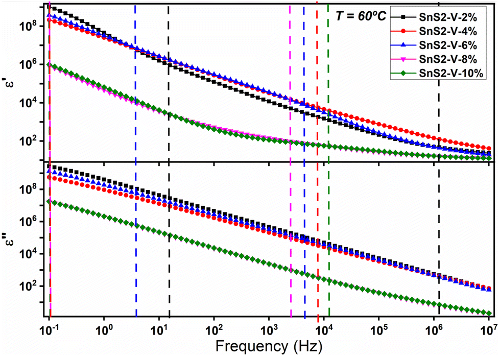 | ||
| Fig. 3 Dielectric spectra for SnS2–V-2% (black), SnS2–V-4% (red), SnS2–V-6% (blue), SnS2–V-8% (magenta) and SnS2–V-10% (olive) at 80 °C. The solid line in the spectrum indicates the value of the fitted curve of the loss permittivity, and the vertical dashed lines indicate the frequency range where the fitting has been made: SnS2–V-2% from 16 to 3 × 10⁶ Hz, SnS2–V-4% from 0.1 to 8 × 10³ Hz, SnS2–V-6% from 4 to 4 × 10³ Hz, SnS2–V-8% from 0.1 to 3 × 10³ Hz and SnS2–V-10% from 0.1 to 1.5 × 10⁴ Hz. | ||
 | ||
Fig. 4 Temperature dependence of free ion diffusion (left) and ionic charge density (right). (■) SnS2–V2%, ( ) SnS2–V4%, ( ) SnS2–V4%, ( ) SnS2–V6%, ( ) SnS2–V6%, ( ) SnS2–V8%, ( ) SnS2–V8%, ( ) SnS2–V10%. ) SnS2–V10%. | ||
Table S2 (ESI†) summarizes the parameters ΔεEP, α and τEP obtained from the fit of Fig. 3. A close inspection of the values tabulated shows that the relaxation time of electrode polarization presents an opposite behavior in case of the samples SnS2–V-2%, SnS2–V-4% and SnS2–V-6%, to SnS2–V-8% and SnS2–V-10% samples. For low vanadium concentration (2, 4 and 6%) the relaxation time increases with increasing temperature, but for high vanadium concentration (8% and 10%) the relaxation time decrease with temperature.
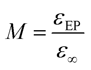
On the other hand, given that the strength of the relaxation given by ΔεEP = εEP −ε∞ is very higher for all the samples and considering that α ≤ 1, which values are compress between 0.9 and 1 in all the samples for all range of temperatures studied. Notice from Table S2 (ESI†) that the jump between the sample permittivity (ε∞) and the electrode polarization εEP is higher, then the interactions do not dominate the transport process, then we can consider that the parameter M can be expressed as
 | (2) |
Taking into account all the above comments and considering that cation and anion have approximately the same mobility together with the Einstein relation for charge diffusivity we can determine the diffusivity as28
 | (3) |
Finally, neglecting ion–ion interactions, the ionic conductivity, σ, containing two types of ions can be expressed as31
| σ = n−e|Z−|μ− + n+e|Z+|μ+ | (4) |
In our system we can consider a mean mobility from the equation μ = (n+μ+ + n−μ−)/n where (n = n+ + n) is the total charge carrier density. Notice that eqn (4) is still valid in the cases where we have a single conductor where only exist one type of ion mobile.
Taking into account the Nernst–Einstein relation between the mobility and diffusion coefficient can be given as
 | (5) |
Then, from eqn (3) and (4) together with Nernst–Einstein relation, given by eqn (6), the free–ion density was obtained as
 | (6) |
Finally, the permittivity values at f → ∞ also named static dielectric permittivity, εr,∞, can be easily obtained as
 | (7) |
Fig. 4 (right) and (left) shows the temperature variation of the diffusivity and mobile charge concentration calculated using the eqn (3) and (6), respectively.
From Fig. 4, panel left, we can see that diffusivity decrease with temperature increase and an abrupt change in the behaviour appears around 80 °C for the samples SnS2–V2% and at 100 °C the sample SnS2–V4%, respectively, where for both samples for these temperatures its diffusivities increasing with temperature increase being the diffusivity of the sample doped with 4% of vanadium around one order of magnitude higher than the other. However, the opposite is observed for the samples of high concentration of vanadium where the samples SnS2–V8% and SnS2–V10% increase the diffusivities with the temperature increase, being its diffusivities between two and three orders of magnitude higher than SnS2–V2% and SnS2–V4%. Notice that such increasing tends to a constant value at higher temperatures above 120 °C. These behaviors are related to the variation of the free ionic charge density. A close inspection of Fig. 4 (panel right), the free ion carrier density varies inversely to the behavior of diffusivity for all the samples studied. For the samples where the amount of vanadium is lower than 6%, the charge carrier density increases until the temperature reach the value of 80 °C, being the value of n (in cm−3) one order of magnitude higher for the sample SnS2–V2% than SnS2–V4% decreasing its values from this temperature. On the other hand, for the samples where the vanadium concentration was 8% and 10% the charge carrier density decreases with temperature increase, being for both samples its values until 5 o six orders of magnitude lower, depending of temperature. These results show that diffusivities are linked to the densities of ion carriers as described in eqn (5).
Finally, we can observe a concentration of vanadium (≅6% V) for which there is a jump, where the behavior of both diffusivity and the charge carriers density does not follow a homogeneous trend. We think that this change is possibly due to large changes in the crystallinity of the Sn or the temperature at which the mixture of vanadium with the SnS2 produces a transition that also generates some type of relaxation, dilation or interaction between the different atoms. That is possible because higher concentrations than 5% of vanadium, a percolation occurs in this type of mixtures.
4. Conclusions
The SnS2 doped with vanadium (V) powders and thin films were magnificently prepared on ITO substrates using a simple and cost-effective hydrothermal technique, making it suitable for large-scale manufacture. Combining previous studies of X-ray diffraction (XRD), scanning electron microscopy (SEM), optical absorbance spectra and electrochemical measurements together with conductivity, diffusivity and charge carriers density, we can conclude that vanadium-doped SnS2 thin films are promising candidates for use as buffer layers in solar cell fabrication. Electrochemical exploration demonstrated that 6% V-doped SnS2 exhibited a meaningful photocurrent comeback (3.0 × 10⁻⁶ A cm−2) associated to pure SnS2 (4.0 × 10⁻⁷ A cm−2). Thus, V-doped SnS2 is a promising material for photovoltaic applications. Additionally, conductivity measurements using electrochemical impedance spectroscopy (EIS) revealed a notable increase in conductivity in samples doped with lower concentrations of vanadium, with a percolation threshold observed around 6% V. This behaviour is quite similar to that observed in Sn1−xCrxS2 samples, where a percolation concentration was noted around 6% Cr. These changes may be attributed to alterations in the crystallinity of SnS2 or changes in the melting temperature of the mixed Sn1−xVxS2 samples, potentially causing relaxation, dilation, or interaction between the different atoms. Our results demonstrate that the vanadium content plays a significant role when mixed with SnS2, suggesting that this material could be a promising candidate, similar to Sn1−xCrxS2, for optoelectronic applications such as photoelectrochemical catalysts, photodetectors, and particularly photovoltaic devices.Data availability
The data that support the findings of this study are available from the corresponding author upon reasonable request.Conflicts of interest
There are no conflicts to declare.Acknowledgements
This work was funded by Generalitat Valenciana through program PROMETEUS, grant CIPROM/2022/03. AG-B thanks the Vicerrectorado de Investigación de la Universitat Politècnica de València, Spain for the financing of the Project (PAID-11-23).References
- K. V. Khot, V. B. Ghanwat, C. S. Bagade, S. S. Mali, R. R. Bhosale, A. S. Bagali, T. D. Dongale and P. N. Bhosale, Synthesis of SnS2 thin film via non vacuum arrested precipitation technique for solar cell application, Mater. Lett., 2016, 180, 23–26 CrossRef CAS.
- P. Jackson, D. Hariskos, E. Lotter, S. Paetel, R. Wuerz, R. Menner, W. Wischmann and M. Powalla, New world record efficiency for Cu (In, Ga) Se2 thin-film solar cells beyond 20%, Prog. Photovoltaics Res. Appl., 2011, 19(7), 894–897 CrossRef CAS.
- K. V. Khot, S. S. Mali, R. R. Kharade, R. M. Mane, P. S. Patil, C. K. Hong, J. H. Kim, J. Heo and P. N. Bhosale, Novel-approach for fabrication of CdS thin films for photoelectrochemical solar cell application, J. Mater. Sci.: Mater. Electron., 2014, 25, 5606–5617 CrossRef CAS.
- C. Shi, P. Yang, M. Yao, X. Dai and Z. Chen, Preparation of SnS2 thin films by close-spaced sublimation at different source temperatures, Thin Solid Films, 2013, 534, 28–31 CrossRef CAS.
- V. R. Reddy, S. Gedi, C. Park, R. W. Miles and K. T. Ramakrishna Reddy, Development of sulphurized SnS thin film solar cells, Curr. Appl. Phys., 2015, 15(5), 588–598 CrossRef.
- F. Jiang, H. Shen, W. Wang and L. Zhang, Preparation of SnS film by sulfurization and SnS/a-Si heterojunction solar cells, J. Electrochem. Soc., 2011, 159(3), H235 CrossRef.
- J. George and C. K. Valsala Kumari, Growth and characterization of tin disulphide crystals grown by physical vapour transport method, J. Cryst. Growth, 1983, 63(2), 233–238 CrossRef CAS.
- K. Kawano, R. Nakata and M. Sumita, Effects of substrate temperature on absorption edge and photocurrent in evaporated amorphous SnS2 films, J. Phys. D: Appl. Phys., 1989, 22(1), 136 CrossRef CAS.
- B. Thangaraju and P. Kaliannan, Spray pyrolytic deposition and characterization of SnS and SnS2 thin films, J. Phys. D: Appl. Phys., 2000, 33(9), 1054 CrossRef CAS.
- W. Du, D. Deng, Z. Han, W. Xiao, C. Bian and X. Qian, Hexagonal tin disulfide nanoplatelets: A new photocatalyst driven by solar light, CrystEngComm, 2011, 13(6), 2071–2076 RSC.
- L. S. Price, I. P. Parkin, A. M. Hardy, R. J. Clark, T. G. Hibbert and K. C. Molloy, Atmospheric pressure chemical vapor deposition of tin sulfides (SnS, Sn2S3, and SnS2) on glass, Chem. Mater., 1999, 11(7), 1792–1799 CrossRef CAS.
- S. Ullah, H. Ullah, S. G. Parra, A. Andrio, B. Mari and V. Compañ, Improvement of optical and conductivity properties of SnS2 via Cr doping for photovoltaic applications, J. Alloys Compd., 2023, 960, 171047 CrossRef CAS.
- S. Ullah, H. Ullah, V. Compañ and B. M. Soucase, Study the Effects of Vanadium (V) Concentration Doped with Tin Disulfide (SnS2), eNergetics, 2022, 127–131 Search PubMed.
- V. Compañ, T. Smith So/rensen, R. Diaz-Calleja and E. Riande, Diffusion coefficients of conductive ions in a copolymer of vinylidene cyanide and vinyl acetate obtained from dielectric measurements using the model of Trukhan, J. Appl. Phys., 1996, 79(1), 403–411 CrossRef.
- (a) J. Vega, A. Andrio, A. A. Lemus, L. F. Del Castillo and V. Compañ, Conductivity study of Zeolitic Imidazolate Frameworks, Tetrabutylammonium hydroxide doped with Zeolitic Imidazolate Frameworks, and mixed matrix membranes of Polyetherimide/Tetrabutylammonium hydroxide doped with Zeolitic Imidazolate Frameworks for proton conducting applications, Electrochim. Acta, 2017, 258, 153–166 CrossRef CAS; (b) R. Coelho, Sur la relaxation d'une charge d'espace, Rev. Phys Appl., 1983, 18, 137–146 CrossRef.
- R. J. Klein, S. Zhang, S. Dou, B. H. Jones, R. H. Colby and J. Runt, Modeling electrode polarization in dielectric spectroscopy: Ion mobility and mobile ion concentration of single-ion polymer electrolytes, J. Chem. Phys., 2006, 124, 144903 CrossRef.
- D. Valverde, A. Garcia-Bernabé, A. Andrio, E. García-Verdugo, S. V. Luis and V. Compañ, Free ion diffusivity and charge concentration on cross-linked polymeric ionic liquid iongel films based on sulfonated zwitterionic salts and lithium ions, Phys. Chem. Chem. Phys., 2019, 21, 17923–17932 RSC.
- S. Ullah, A. Bouich, H. Ullah, B. Mari and M. Mollar, Enhanced optical and structural properties of V-doped binary SnS2 buffer layer, Sol. Energy, 2020, 204, 654–659 CrossRef CAS.
- D. Nuevo, M. Cuesta, R. Porcar, A. Andrio, E. Garcia-Verdugo and V. Compañ, Novel electrolytes based on mixtures of dimethyl sulfoxide task specific zwitterionic ionic liquid and lithium salts: Synthesis and conductivity studies, Chem. Phys., 2023, 575, 112043 CrossRef CAS.
- G. Zhu, M. Hojamberdiev, W. Zhang, S. T. U. Din, Y. J. Kim, J. Lee and W. Yang, Enhanced photocatalytic activity of Fe-doped Bi4O5Br2 nanosheets decorated with Au nanoparticles for pollutants removal, Appl. Surf. Sci., 2020, 526, 146760 CrossRef CAS.
- V. Compañ, J. Escorihuela, J. Olvera, A. García-Bernabé and A. Andrio, Influence of the anion on diffusivity and mobility of ionic liquids composite polybenzimidazol membranes, Electrochim. Acta, 2020, 354, 136666 CrossRef.
- F. Plasser, S. Gómez, M. F. S. J. Menger, S. Mai and L. González, Highly efficient surface hopping dynamics using a linear vibronic coupling model, Phys. Chem. Chem. Phys., 2019, 21(1), 57–69 RSC.
- T. S. Sorensen and V. Compañ, Complex permittivity of a conducting, dielectric layer containing arbitrary binary Nernst–Planck electrolytes with applications to polymer films and cellulose acetate membranes, J. Chem Soc., Faraday Trans., 1995, 91, 4235–43250 RSC.
- T. S. Sorensen, V. Compañ and R. Diaz-Calleja, Complex permittivity of a film of poly[4-(acryloxy)phenyl-(4-chlorophenyl)methanone] containing free ion impurities and the separation of the contributions from interfacial polarization, Maxwell–Wagner–Sillars effects and dielectric relaxations of the polymer chains, J. Chem. Soc., Faraday Trans., 1996, 92, 1947–1957 RSC.
- J. R. Macdonald, Theory of ac Space-Charge Polarization Effects in Photoconductors, Semiconductors, and Electrolytes, Phys. Rev., 1953, 92, 4 CrossRef CAS.
- C. Krause, J. R. Sangoro, C. Iacob and F. J. Kremer, Charge transport and dipolar relaxations in imidazolium-based ionic liquids, J. Phys. Chem. B, 2010, 114, 382 CrossRef CAS PubMed.
- D. Fragiadakis, S. Dou, R. H. Colby and J. Runt, Molecular mobility and Li+ conduction in polyester copolymer ionomers based on poly(ethylene oxide), J. Chem. Phys., 2009, 130, 064907 CrossRef.
- A. Serguei, M. Tress, J. R. Sangoro and F. Kremer, Electrode polarization and charge transport at solid interface, Phys. Rev. B: Condens. Matter Mater. Phys., 2009, 80, 184301 CrossRef.
- A. Andrio, S. I. Hernández, C. García-Alcántara, L. F. Del Castillo, V. Compañ and I. Santamaría-Holek, Temperature dependence of anomalous protonic and superprotonic transport properties in mixed salts based on CsH2PO4, Phys. Chem. Chem. Phys., 2019, 21, 12948 RSC.
- A. S. Saplov, R. Marcilla and D. Mecerreyes, Recent advances in innovative polymer electrolytes based on poly(ionic liquid)s, Electrochim. Acta, 2015, 175, 18 CrossRef.
- T. M. W. J. Bandara, M. A. K. L. Dissanayake, O. A. Ileperuma, K. Varaprathan, K. Vignarooban and B.-E. Mellander, Polyethyleneoxide (PEO)-based, anion conducting solid polymer electrolyte for PEC solar cells, J. Solid State Electrochem., 2008, 12, 913–917 CrossRef CAS.
- T. M. W. J. Bandara, M. A. K. L. Dissanayake, I. Albinsson and B.-E. Mellander, Evaluation of mobility, diffusion coefficient and density of charge carriers in ionic liquids and novel electrolytes based on a new model for dielectric response, Solid State Ionics, 2011, 189, 63 CrossRef CAS.
Footnote |
| † Electronic supplementary information (ESI) available. See DOI: https://doi.org/10.1039/d5cp01255d |
| This journal is © the Owner Societies 2025 |