Unlocking the sensing and scavenging potential of Sc2CO2 and Sc2CO2/TMD heterostructures for phosgene detection†
Received
14th February 2025
, Accepted 31st March 2025
First published on 1st April 2025
Abstract
The detection of phosgene is critically important owing to its extreme toxicity and potential use as a chemical warfare agent to ensure public safety and security. Two-dimensional (2D) scandium carbide MXenes (Sc2CTx; T = O−, x = 2) stand out as promising materials for gas sensing applications owing to their unique electronic and adsorption properties. In this study, first-principles calculations based on the GGA-PBE functional were employed to investigate the structural, electronic, and mechanical characteristics of Sc2CO2 with different surface termination positions. The adsorption behavior of Sc2CO2 was systematically explored for various gas molecules, including N2, O2, CO, NO, CH4, H2S, and, notably, phosgene (COCl2). Specifically, phosgene exhibited a high adsorption energy, highlighting the selectivity of Sc2CO2 towards this toxic gas. Furthermore, the impact of gas adsorption on the electronic structure of Sc2CO2 was investigated. Strategies such as increasing the operating temperatures and forming heterostructures with transition metal di-chalcogenides (MoSe2 and WSe2) proved to be highly effective to mitigate the challenges related to slow recovery time. Thus, this work underscores the potential of Sc2CO2 MXenes as highly sensitive and selective gas sensors, particularly for phosgene sensing.
1. Introduction
Phosgene (COCl2) is a highly toxic volatile irritant used in pharmaceuticals and agricultural applications such as in pesticides.1 It is a volatile liquid, which is gaseous at room temperature.2 According to the National Institute for Occupational Safety and Health (NIOSH), its safe exposure limit is 0.1 ppm.3 Furthermore, no antidotes for this toxic chemical have been invented yet.4 Therefore, its immediate detection is crucial in order to avoid any severe trauma or accident. To date, the fluorimetric detection method is the pronounced detection method for phosgene.5–8 However, it suffers from fluorescence bleaching and signal crosstalk.9 Chang et al. conducted a theoretical study to analyse the chemiresistive detection of phosgene using arsenene as the sensing material.10 However, not many nanomaterials have been explored in the detection of phosgene, which may be because of its inertness toward receptor surfaces. Therefore, there is a quest for new nanomaterials for developing phosgene sensors.
MXene is an artificially developed two-dimensional material that has gained significant importance in sensing.11 It has the chemical formula of Mn+1XnTx, where M is the transition metal, X is either C or N or S, and Tx is the functional group (–OH, –F, and –O). It has been used in sensing different analytes and has applications in wearable and flexible electronics for health monitoring.12 Most of the MXenes exhibit a metallic nature, which limits their applications in chemiresistive sensing. However, the metallic nature can also be channelized to improve the sensing. Kim et al. have reported metallic Ti3C2Tx for the detection of volatile organic compounds with a limit of detection of less than 100 ppb at room temperature.13 The functional group present on the MXene surface leads to an improvement in the signal-to-noise ratio. Hence, it has also found its application in self-powered electronic devices.14–16 Thomas et al., through density functional theory (DFT) studies, have found that an –OH-functionalized Ti2C MXene has decent sensitivity towards phosgene detection.17 Similarly, a molybdenum-based MXene (Mo2C) studied using DFT had shown good response towards chemical warfare agents.18 Sulfur- and fluorine-functionalised molybdenum-based MXenes exhibited higher binding than oxygen-functionalised Mo2C. Other 2D materials such as metal-decorated phthalocyanine monolayers also showed sensitivity towards phosgene.19 Similarly, Yang et al. have reported sensing of reducing gases using pristine and Mn-doped Sc2CO2.20 Motivated by the studies reported in the literature, we chose to explore Sc2CO2 MXenes for phosgene detection. Through both theoretical and experimental studies, it is claimed that the Sc2C MXene shows a semiconducting nature.21 Even its band gap was modulated from indirect to direct through material engineering. Chen et al. reported the first experimentally synthesized 2D Sc2COx MXene using magnetron sputtering to study its optical properties.22 It was found that the bandgap of the material increased with the increase in annealing temperature. Further, it becomes scandium oxide at higher annealing temperatures.
MXene-based sensors with structural modulation, intercalation, and formation of heterostructures have been used in order to improve sensitivity, selectivity, and stability.23,24 Transition metal dichalcogenides (TMDs) are a class of vdW materials that have the potential in gas sensing as well as the formation of heterojunctions with other materials.25,26 They have the chemical formula MX2, where M is a transition metal (W, Mo, etc.) and X is a chalcogen (S, Se, and Te). Recently, Janus transition metal dichalcogenides have been tried for sensing phosgene gas.27 Several reports in both theoretical and experimental research support the heterostructures of MXenes and TMDs for sensing VOCs and other gas molecules.28–30 MXenes have been tried with different other materials such as oxides and perovskites for various applications including sensing.31 Two-dimensional vertical heterostructures, created by stacking various 2D materials, demonstrate diverse vertical properties in material engineering.32 van der Waals (vdW) heterostructures help to overcome difficulties faced by materials as well as improve the sensing ability.33 Reportedly, the formation of Ti3C2Tx/SnS2 heterostructures has shown improved sensitivity as well as long-term stability of the MXene. As the MXene has a tendency to get oxidised, the formation of the heterostructure inhibited oxidation for a long time.34
It is a fact that the experimental analysis of this kind of gas is risky and it needs proper arrangement in order to perform testing under laboratory conditions. Therefore, theoretical modelling is a rational choice to analyse the sensing mechanism of such gas. The density functional theory (DFT) plays a pivotal role in gas sensing research, providing valuable insights into surface–adsorbate interactions,35,36 including the analysis of material stability. For instance, Yorulmaz et al. confirmed the stability of different MXene structures including Sc2CO2 through phonon dispersion calculations.37 Opoku et al. reported the kinetic and thermal stability of g-GaN/Sc2CO2 heterostructures using phonon dispersion and molecular dynamics calculations.38 This article presents the pristine Sc2CO2 monolayer-based phosgene detection using density functional theory. The structural, electronic, and elastic properties of unit cell structures are analysed in detail to apply the material for sensing. This work demonstrates that the COCl2 molecule on the Sc2CO2 MXene has a suitable adsorption strength and explicit charge transfer compared to other targeted molecules. Moreover, the influences of vertically stacked WSe2/Sc2CO2 and MoSe2/Sc2CO2 2D-heterostructures on phosgene sensing are explored. In the subsequent sections, the details of computational methods followed by results obtained from the study are discussed explicitly. To the best of our knowledge, this is the first study on the detection of phosgene using a Sc2CO2 monolayer and its heterostructures with TMDs such as WSe2 and MoSe2. Hence, the novel findings from this study are likely to provide a reference for phosgene sensor devices.
2. Computational methods
Density functional theory calculations were conducted using the Vienna ab initio simulation package (VASP).39 Structural models were generated using the Vesta software.40 The generalised gradient approximation of Perdew–Burke–Ernzerhof (GGA-PBE) was adopted for the exchange–correlation potential to estimate the interaction of different elements such as atoms and ions to carry out calculations for evaluating all the properties.41 It is well known that GGA-PBE is the widely used functional for evaluating the electronic properties, as it provides adequate balance between computation cost and accuracy. Several works have been reported in modelling 2D material-based monolayers and heterostructures using this functional.42–45 Therefore, we chose this functional to describe the exchange–correlation interaction. The Monkhorst–Pack scheme with a 3 × 3 × 1 grid sampled the Brillouin zone. A plane wave cut-off of 520 eV was applied throughout the calculations. Structural optimization was fully achieved with convergence criteria set at 10−5 eV for total energy and 0.01 eV Å−1 for residual force. A 21 Å vacuum space along the c-axis of the MXene monolayer structure was used to prevent interlayer interactions during periodic DFT calculations. We used DFT-D3 dispersion correction to account for van der Waals interactions in monolayers and heterostructures.42,46 However, it is known that vdW interaction is more effective in multilayer structures, while in monolayer structures, its effect is insignificant.47 The charge transfer between MXenes and interacting molecules was evaluated using the Vesta software. The electronic properties such as density of states spectra and band structure were calculated using the PBE functional. No significant effect due to dipole was observed in the structures with a 21 Å vacuum gap. The results were verified with reported ref. 48 and 49, where the 20 Å vacuum gap was applied to optimize the structures, and the influence of dipole corrections was evaluated.49 For the molecular dynamics study, we used the BURAI software to perform the simulation.50
3. Results and discussion
3.1 Sc2CO2 bulk
3.1.1 Structural and electronic properties of Sc2CO2 bulk.
As the crystallographic database for the unit cell of oxygen (–O)-functionalised Sc2C– is not available, we optimized the structure by placing oxygen atoms at different positions. Here, we tried four different models named struct_1, struct_2, struct_3, and struct_4. The optimized bulk structures of Sc2CO2 are presented in Fig. 1.
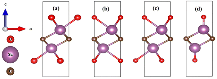 |
| | Fig. 1 Side view of the bulk structures of different models of Sc2CO2: (a) struct_1, (b) struct_2, (c) struct_3, and (d) struct_4. The direction arrows at the left represent the lattice direction of the structures. | |
The 3D representation of these bulk structures is presented in the ESI† (Fig. S1). The circles in red, violet, and dark brown colors represent oxygen (O), scandium (Sc), and carbon (C) atoms, respectively. The supercell structures of each model are presented in Fig. S2 of the ESI.† The unit cells for each model were selected through an energy convergence test, and their stability was found to be in the order of struct_3 > struct_2 > struct_4 > struct_1. The lattice parameters of the unit cell are a = b = 3.44393 Å, c = 10.07122 Å, α = β = 90°, and γ = 120°, and these parameters have great resemblance with the reported results.51 The atomic position of each atom in the respective unit cell is provided in the ESI† (Table S1). It is a trigonal structure with the space group P3.
The formation energy (Ef) of the structures, which explains their stability, was estimated, based on the following formula:52
| |  | (1) |
where
E0(MCO) is the total energy of the MXene surface,
E0(M) is the total energy of the metal atom,
E0(C) is the total energy of the carbon atom, and
E0(O) is the total energy of the oxygen atom,
nM is the number of metal atoms,
nC is the number of carbon atoms,
nO is the number of oxygen atoms, and
N is the number of MXene atoms.
The calculated values of Ef for struct_1, struct_2, struct_3, and struct_4 are, −1.322, −2.645, −2.688, and −1.118 (in eV) respectively. In order to use these structures for gas sensing, the electronic properties such as band gap and nature of the material need to be known. Therefore, the band structure and density of states were calculated using DFT. The projected total density of states with the band structure of each molecule is presented in Fig. 2.
 |
| | Fig. 2 Band structure and projected DOS spectra of the Sc2CO2 unit cell: struct_1, struct_2, struct_3 and struct_4. | |
The Fermi level was set to 0 eV for all calculations. Moreover, the range of the energy band in DOS and band structures is kept between −5 and +5 eV throughout the article, as bands far away from the Fermi level do not contribute to the physical and chemical properties of any material.53 The k-path for band structure calculation in the first Brillouin zone was Γ–M–K–Γ, as obtained using VASPKIT.54 In the case of struct_1, it can be observed from both the band structure and density of states spectra that continuous bands are present in both the valence and conduction bands. This signifies the metallic nature of the material.55 The structures struct_2 and struct_3 both exhibited semiconducting nature with indirect band gaps of 1.996 eV and 1.778 eV respectively. The calculated Fermi energy level for struct_2 and struct_3 are 0.23 eV and 0.227 eV away from the valence band maximum, and 1.766 eV and 1.551 eV away from the conductance band minimum, respectively. From this, it can be observed that they exhibit p-type semiconducting nature.56 The band gap for oxygen-functionalised MXenes was verified from the reported results.31,57 In addition, it was found that both spin-up and spin-down states are symmetric. This confirms the non-magnetic nature of the materials.58 The struct_4 model has shown completely different dynamics. It can be seen that spin up bands shows semiconducting nature with a band gap of 1.64 eV, while, the spin-down states exhibit metallic nature as bands near the Fermi level are present in both valence and conduction bands. Therefore, this structure demonstrates a half-metallic nature and holds significant promise for applications in spintronics.53,59,60 Another important parameter in gas sensing materials is the effective mass (m*) of the carriers present in the material. Here, we also estimated the value of m* from the band structure of struct_2 and struct_3 using the following equation:61
| |  | (2) |
where ‘
E’ is the electron energy along the wave vector ‘
k’ and ‘
ħ’ is the reduced Planck constant. The observed effective mass of electrons for struct_2 and struct_3 was found to be 2.5
m0 and 7.92
m0 respectively, where
m0 is the rest mass of an electron. Similarly, the hole effective mass of struct_2 and struct_3 was ascertained to be 7.92
m0 and 10.29
m0, respectively. Since the mobility of carriers and their effective mass are inversely proportional,
62,63 therefore, it can be estimated that both electron and hole mobilities are larger in struct_2, which makes it comparatively efficient in charge transport, and hence, makes it suitable for gas sensing.
64 As a part of this work, we considered only the structures with a semiconducting nature. The semiconducting materials are preferred because they allow the control flow of carriers through the device and sensing can be done depending on the observed variation in parameters such as resistance and work function.
65 Based on the carrier's effective mass and the semiconducting nature, the model struct_2 was considered for further study. However, struct_3 can also be a great choice for various applications including sensing.
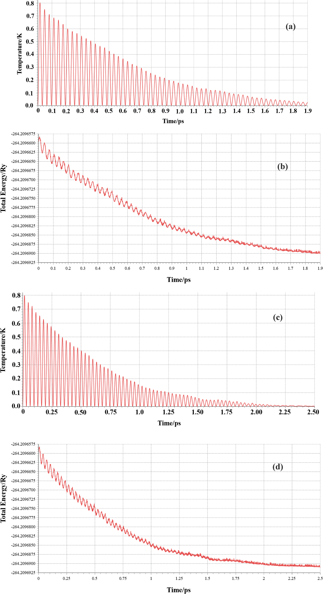
To check the thermodynamic stability, we performed the molecular dynamics calculations of struct_2 and struct_3. We used the Born–Oppenheimer molecular dynamics (BOMD) method with a velocity rescaling thermostat scheme at a temperature of 300 K for ∼2.5 ps and 1.2 fs time step. The temperature variation with time between 0 and 2.5 picoseconds, as shown in Fig. 3(a) and (c), illustrates their thermal stability. Similarly, the total energy was found to fluctuate around a constant energy value (Fig. 3(b) and (d)). This explains that the systems are stable. Even, the energy variation and temperature fluctuation are correlated, which suggest the correct response of the systems with thermal changes. Even from the MD movie analysis no breaking of bonds was observed, which confirms its stability.
 |
| | Fig. 3 Molecular dynamics calculation: (a) temperature variation of struct_2, (b) total energy variation of struct_2, (c) temperature variation of struct_3, and (d) total energy variation of struct_3. | |
3.1.2 Elastic properties.
Although mechanical properties such as bulk modulus (K), shear modulus (G), and Young's modulus (E) are not the foremost factors in selecting sensing materials, they remain pertinent in specific contexts, particularly concerning long-term durability and reliability. In cases where the sensing mechanism involves a change in mechanical strain affecting resistance, these moduli become significant.57 The behavior of a material under external influences such as pressure and strain is dictated by its elastic characteristics, encompassing factors like bonding between atoms, stability under mechanical stress, phonon modes, and other solid-state phenomena.66 These attributes are critical for diverse applications, including novel areas such as gas detection, where changes in elasticity are exploited.67,68 Elastic properties are mathematically described by second-order partial derivatives of total energy with respect to strain, as outlined in the reference provided.69 As these materials are theoretically modelled and their experimental parameters are yet to be validated, it is important to check the mechanical stability of the material. Here, we calculated the elastic properties of struct_2 and struct_3 models. The details of the calculated parameters are given in Table 1. Further, their mechanical stability was tested by calculating the elastic properties of the materials. Both structures are found to be mechanically stable as per the conditions for stability as mentioned below (inequality (i)–(iv)).70 It can be seen that the struct_2 model is less prone to mechanical deformation.| | | C132 < 0.5 × C33(C11 + C12) | (ii) |
| | | C142 < 0.5 × C44 × (C11 − C12) | (iii) |
Table 1 Calculated elastic coefficients (Cij), and other derived parameters such as bulk modulus (K), shear modulus (G), and Young's modulus (E) in giga pascal (GPa)
|
|
C
11
|
C
12
|
C
13
|
C
14
|
C
33
|
C
44
|
C
66
|
K
|
G
|
E
|
| Struct_2 |
69.57 |
33.74 |
1.47 |
0.074 |
2.21 |
2.82 |
17.91 |
23.86 |
11.69 |
30.14 |
| Struct_3 |
64.65 |
33.39 |
2.08 |
0.475 |
2.38 |
0.88 |
15.63 |
22.98 |
9.75 |
25.63 |
3.2 Sc2CO2 monolayer
3.2.1 Structural and electronic properties of Sc2CO2 monolayers.
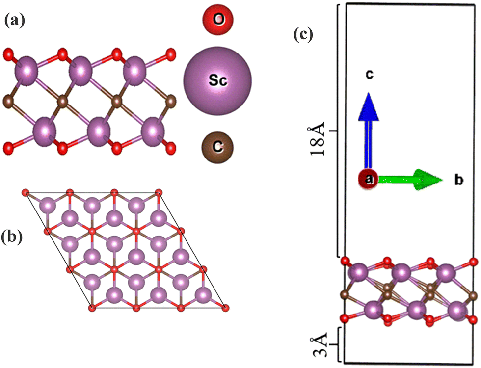
One of the most important features that attracts researchers in delving deep into MXene-based materials for gas sensing and other applications is their two-dimensional sheet-like structures.20,21 An excessive number of layers could potentially trap interacting gas molecules, leading to diminished sensor performance due to reduced surface exposure and slower gas molecule diffusion. So to begin with the analysis of material properties, the Sc2CO2 monolayer was formed using struct_2 by adding a vacuum layer of 21 Å and the structure was optimized by relaxing the ions in order to get the most stable structure. The optimized 3 × 3 × 1 monolayer of Sc2CO2 is shown in Fig. 4. Struct_2 model was used for making the monolayer and further study was continued.
 |
| | Fig. 4 Sc2CO2 monolayer structure: (a) side view, (b) top view, and (c) side view with 21 Å vacuum. | |
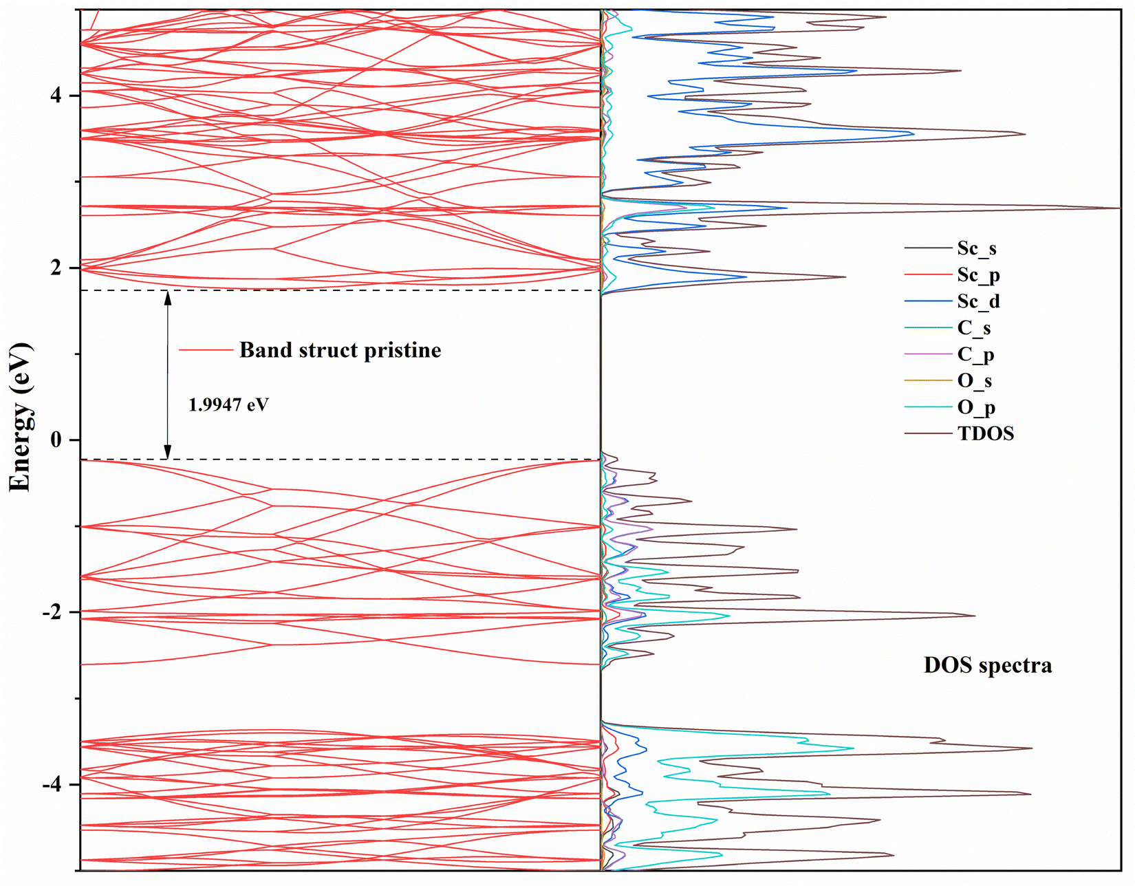
Then, the electronic properties of the materials were observed using density of states spectra and band structure, as shown in Fig. 5. It was found that the bandgap of the Sc2CO2 monolayer is 1.9947 eV, which is slightly smaller than that of its bulk counterpart. Typically, monolayer structures exhibit a higher bandgap than that of their bulk counterparts. However, there are also reports where monolayer materials display a lower bandgap.71 The insignificant variation in bandgap (1.2 meV) may be due to strong decoupling of the Sc2CO2 monolayer with other layers. Moreover, the decrease in the energy gap may be due to the dominant effect of lattice relaxation over the quantum confinement effect on the monolayer as compared to the bulk. From Fig. S3 of the ESI,† it can be seen that there is a left shift of Sc_d orbitals in the monolayer and new peaks appear near the conduction band minimum. It confirms the electron transfer between Sc_d orbitals and O_p orbitals near the conduction band minimum, which leads to a decrease in bandgap in the monolayer structure.72
 |
| | Fig. 5 Band structure and projected density of states (eV per atoms) of the Sc2CO2 monolayer. | |
The valence band is mainly formed due to the strong hybridisation of C_p and Sc_d orbitals. A significant contribution from O_p orbitals can also be seen, whereas the conduction band is largely formed by Sc_d and O_p orbitals. The band structure (Fig. 5) displays an indirect bandgap with electron and hole effective masses of 8.68m0 and 25.33m0, respectively. It can be observed that there is an almost more than three times increase in effective mass in the monolayer.
3.2.2 Adsorption of CO, NO, CH4, H2S, COCl2, O2, and N2 Gas molecules on the Sc2CO2 monolayer.
The interaction of gas molecules with any sensing material was estimated from parameters such as adsorption energy, variation in conductivity, and charge transfer between the adsorbate and the adsorbent. In order to evaluate the adsorption energy, it is mandatory to measure the total energy as per the formula mentioned in eqn (3). The adsorption energy (Ead) of the molecule was calculated using the following formula:| | | Ead = Eadsorbate+adsorbent − Eadsorbate − Eadsorbent | (3) |
where Eadsorbate+adsorbent is the total energy of the complex of sensing material and target gas, Eadsorbate is the total energy of the target gas, and Eadsorbent is the total energy of the sensing material. All the energy values were calculated by keeping the size of the monolayer fixed.
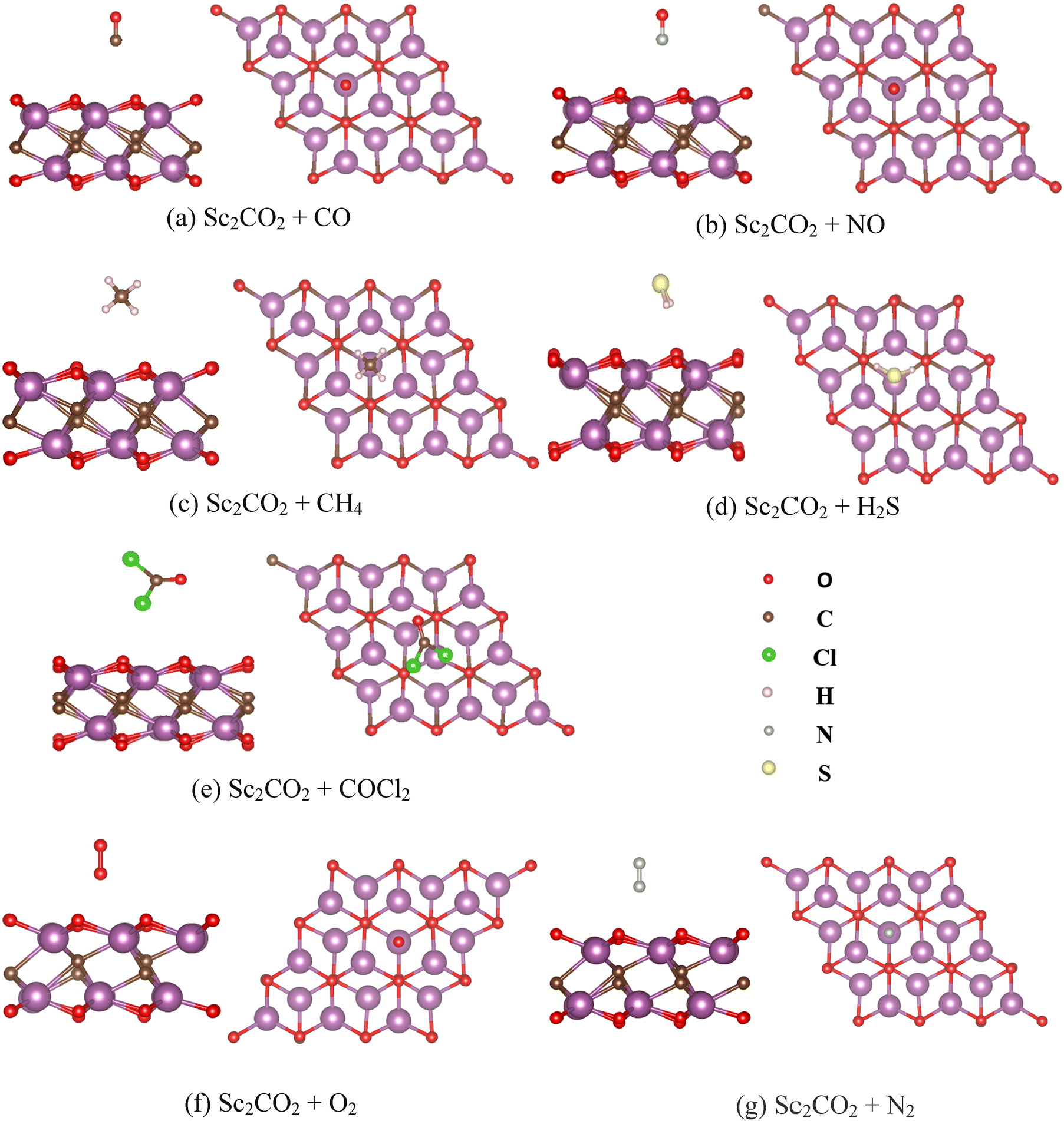
The side view and top view of the optimised Sc2CO2 monolayer structures after interacting with CO, NO, CH4, H2S, COCl2, O2, and N2 are shown in Fig. 6. The calculated adsorption energy (without van der Waals correction) of CO, NO, CH4, H2S, COCl2, O2, and N2 on the surface of the Sc2CO2 monolayer is tabulated in Table S2 (ESI†). It can be observed that all the molecules exhibited negative adsorption energy and the phosgene molecule has the largest adsorption energy (1.97 eV) among them. This signifies the selective detection and strong interaction of COCl2 on the Sc2CO2 surface. However, the distance between the gas molecule and the sensing material did not show any common trend with respect to the adsorption energy. In order to observe the influence of van der Waals interaction, we also optimised the monolayer with the DFT-D3 correction and calculated the adsorption energy and charge transfer upon interaction with target gas molecules. The calculated results are mentioned in Table 2. Although there is a change in magnitude of Ead due to van der Waals correction, the trend is the same as the non-van der Waals corrected data. The adsorption energy values with vdW correction were found to be reasonable. We added the adsorption energy without vdW in the ESI† (Table S2) to show the significance of vdW correction in such structures, which will be beneficial for readers in structural property analysis.
 |
| | Fig. 6 Side and top views, respectively, of (a) Sc2CO2 + CO, (b) Sc2CO2 + NO, (c) Sc2CO2 + CH4, (d) Sc2CO2 + H2S, (e) Sc2CO2 + COCl2, (f) Sc2CO2 + O2, and (g) Sc2CO2 + N2. | |
Table 2 Calculated distance (d) of the gas from the MXene surface, adsorption energy (Ead) with vdW correction, charge transfer (Δq), recovery time (τ) at 298 K and 373 K, and bandgap (Eg), of CO, NO, CH4, H2S, COCl2, O2, and N2 after interaction with Sc2CO2, and conductivity (σ)
| Model |
d (Å) |
E
ad (eV) |
Δq (e) |
τ (s)/298 K |
τ (s)/373 K |
E
g (eV) |
σ
|
| Sc2CO2 |
— |
— |
— |
— |
— |
1.995 |
X |
| Sc2CO2 + O2 |
1.6 |
−0.128 |
0.099 |
1.455 × 10⁻¹⁰ |
5.35 × 10⁻¹¹ |
— |
— |
| Sc2CO2 + CO |
2.98 |
−0.146 |
−0.006 |
2.93 × 10⁻¹⁰ |
9.35 × 10⁻¹¹ |
1.37 |
1.98X |
| Sc2CO2 + N2 |
1.5 |
−0.152 |
0.016 |
3.69 × 10⁻¹⁰ |
1.13 × 10⁻¹⁰ |
1.41 |
2.02X |
| Sc2CO2 + NO |
2.49 |
−0.164 |
0.049 |
5.90 × 10⁻¹⁰ |
1.635 × 10⁻¹⁰ |
— |
— |
| Sc2CO2 + CH4 |
2.53 |
−0.424 |
0.05 |
1.46 × 10⁻⁵ |
5.3 × 10⁻⁷ |
1.29 |
1.91X |
| Sc2CO2 + H2S |
2.14 |
−0.941 |
0.107 |
7.93 × 10³ |
5.04 |
1.25 |
1.87X |
| Sc2CO2 + COCl2 |
3.00 |
−1.130 |
−0.005 |
1.23 × 10⁷ |
1.78 × 10³ |
1.24 |
1.86X |
| WSe2_Sc2CO2 |
— |
|
|
— |
— |
0.88 |
1.55X |
| WSe2_Sc2CO2 + COCl2 |
1.6 |
−0.458 |
1.867 |
5.4 × 10⁻⁵ |
1.5 × 10⁻⁶ |
0.6 |
1.35X |
| MoSe2_Sc2CO2 |
— |
|
|
— |
— |
0.65 |
1.38X |
| MoSe2_Sc2CO2 + COCl2 |
1.8 |
−0.653 |
1.789 |
1.07 × 10⁻¹ |
6.5 × 10⁻⁴ |
0.5 |
1.28X |
Another important parameter crucial in designing a gas sensor is the recovery time (τ). The recovery time of the sensor is related to the amount of adsorption energy (Ead) of the gas on the sensing surface. The mathematical expression of recovery time (τ) is given below:19
| |  | (4) |
where
ν0 is the attempt frequency (10
12 s
−1),
kB is the Boltzmann constant, and
T is the operating temperature.
46 Based on the above equation (
eqn (4)), the recovery time for each gas at room temperature (298 K) and 373 K was calculated, and the results are presented in
Table 2. It can be observed that due to the strong interaction, the material tends to hold the gas on the MXene surface for a longer period of time, if operated at room temperature. However, at 373 K, the recovery of the CO sensor becomes 244 s, and shows the possibility of using this as the reusable sensor. For NO, COCl
2, H
2S, and CH
4, the recovery time is quite large at both 298 K and 373 K temperatures. Therefore, this may not be suitable for reusable gas sensors, but it can used for the removal of these gas molecules, especially COCl
2.
19
Further, the interaction of each of these gas molecules on the Sc2CO2 monolayer was analysed using density of states spectra. It is to be noted that the orbitals near the conduction band minimum and valence band maximum are the major factors in the band gap variation.21 The conduction bands of the total density of states (TDOS) for CO-interacted MXenes are mainly contributed by the Sc_d partial density of states, as shown in Fig. 7(a). Moreover, a strong hybridisation of C_p and O_p states is visible. Since elements present in both the adsorbate and the adsorbent are common, their distinct contribution in DOS is not possible. However, it can be observed that the estimated bandgap reduced to 1.37 eV and the contribution of carbon p orbitals in the conduction band is more pronounced. Unlike all other gas molecules, the DOS profile of NO-interacted Sc2CO2 (Fig. 7(b)) exhibited an asymmetric profile for spin-up and spin-down electrons. This confirms the introduction of magnetic nature in NO-adsorbed Sc2CO2.73 The variation in magnetic moment (m) upon interaction of NO gas suggests that Sc2CO2 could serve as a magnetic gas sensor.74 The change (Δm) arising from NO gas adsorption can also be used to measure the sensitivity of the gas sensor. This potential is based on the analysis of individual molecules, but further investigation is required to understand how magnetization varies with the NO concentration. The contribution of each element present in NO in magnetisation was calculated, and is reported in Table 3. It can be seen that after interacting with NO, the material starts to behave like metal. The TDOS around the Fermi level was contributed by N_p and O_p orbitals, as can be seen from Fig. 7(b).
 |
| | Fig. 7 (a) Total and partial density of states of Sc2CO2 + CO. (b) Total and partial density of states of Sc2CO2 + NO. (c) Total and partial density of states of Sc2CO2 + CH4. (d) Total and partial density of states of Sc2CO2 + H2S. (e) Total and partial density of states of Sc2CO2 + COCl2. (f) Total and partial density of states of Sc2CO2 + O2. (g) Total and partial density of states of Sc2CO2 + N2. | |
Table 3 Calculated magnetic moment (m) expressed in Bohr magnetron (μB) of NO gas after interaction with Sc2CO2 and contribution of each orbital
| NO |
s (μB) |
p (μB) |
d (μB) |
Total (μB) |
| O |
0.003 |
0.257 |
0.0 |
0.260 |
| N |
0.012 |
0.457 |
0.0 |
0.469 |
| Total |
0.015 |
0.714 |
0.0 |
0.729 |
From the DOS spectra of CH4 (Fig. 7(c)), the bandgap of the material was found to 1.29 eV. The valence and conduction bands are similar to those of pristine Sc2CO2. The interaction of CH4 can be observed from the change in the bond length of Sc–C and Sc–O. Similarly, the interaction of H2S led to a reduction in bandgap to 1.25 eV (Fig. 7(d)). Here, the S_s orbitals of H2S contributed significantly to the valence band. In the case of COCl2 (Fig. 7(e)), there was the largest shift in the bandgap. The interaction of COCl2 near the band extremum was found to be contributed by C_p and O_p states. However, Cl_p states can be seen contributing ∼2 eV. The DOS spectra of the O2 interacted structure (Fig. 7(f)) reveal the metallic nature of the overall structure. The bands near the zero energy level are contributed by the C_p and O_ p orbitals. The N2-interacted structure shows (Fig. 7(g)) semiconducting nature with a band gap of 1.4 eV. The details of structural parameters such as bond-length of Sc2CO2 and interacting gas molecules are presented in Table 4. It can be observed that there is a change in the bond length due to the interaction of gas molecules.
Table 4 Calculated bond lengths of different bonds after interaction with CO, NO, CH4, H2S, COCl2, O2, and N2
| Structure |
Bond |
Bond length (Å) |
| Pristine Sc2CO2 |
Sc–C |
2.384 |
| Sc–O |
2.12 |
| COCl2 |
C–O |
1.197 |
| C–Cl |
1.735–1.751 |
| Sc2CO2–CO |
Sc–C |
2.28–2.49 |
| Sc–O |
2.05–2.16 |
| C–O |
1.145 |
| Sc2CO2–NO |
Sc–C |
2.28–2.5 |
| Sc–O |
2.05–2.14 |
| N–O |
1.175 |
| Sc2CO2–CH4 |
Sc–C |
2.27–2.5 |
| Sc–O |
2.05–2.2 |
| C–H |
1.1 |
| Sc2CO2–H2S |
Sc–C |
2.275–2.49 |
| Sc–O |
2.1–2.25 |
| H–S |
1.355, 1.3565 |
| Sc2CO2–COCl2 |
Sc–C |
2.31–2.42′ |
| Sc–O |
2.06–2.18 |
| C–O |
1.2 |
| C–Cl |
1.75 |
| Sc2CO2–O2 |
Sc–C |
2.27–2.42 |
| Sc–O |
2.05–2.2 |
| O–O |
1.23959 |
| Sc2CO2–N2 |
Sc–C |
2.05–2.2 |
| Sc–O |
2.05–2.16 |
| N–N |
1.11315 |
| MoSe2–Sc2CO2 |
Sc–C |
2.249–2.465 |
| Sc–O |
2.04–2.14 |
| Mo–Se |
2.555–2.559 |
| MoSe2–Sc2CO2–COCl2 |
Sc–C |
2.25–2.5 |
| Sc–O |
2.06–2.14 |
| C–Cl |
1.74 |
| C–O |
1.205 |
| Mo–Se |
2.557 |
| WSe2–Sc2CO2 |
Sc–C |
2.245–2.5 |
| Sc–O |
2.05–2.155 |
| W–Se |
2.561–2.564 |
| WSe2–Sc2CO2–COCl2 |
Sc–C |
2.25–2.5 |
| Sc–O |
2.05–2.158 |
| C–Cl |
1.731, 1.732 |
| C–O |
1.202 |
| W–Se |
2.562–2.563 |
We can also estimate the sensing by observing the variation in electrical conductivity (σ) of the material after interaction using eqn (5):19
| |  | (5) |
where the symbols have their usual meaning. Considering “X” to be the conductivity of the Sc
2CO
2 monolayer before interaction, we estimated the conductivity after the interaction of each gas and presented in
Table 2, provided that the variation in bandgap (
Eg) due to temperature (
T) change is not considered. It can be inferred from the data obtained in
Table 2 that the interaction of all gas molecules (N
2, O
2, CO, NO, CH
4, H
2S, and COCl
2) has influence on the resistivity of the Sc
2CO
2 monolayer and, hence, shows good sensitivity.
Upon adsorption onto the surface, the electronic structures of the entire system undergo modifications, resulting in a redistribution of charges between the gas molecule and the sensing material. To do further analyses, Bader charge calculations were employed to quantify the electron distribution across individual atoms, revealing the amount of charge transfer induced by the adsorption of gas molecules. The transfer of charges from the Sc2CO2 monolayer to gas molecules was quantified by comparing the total charges before and after interaction using first-principles calculations. In Table 2, the charge transfer (Δq), indicating either a gain (indicated by a minus sign) or a loss (indicated by a plus sign) of charge for Sc2CO2 upon interaction with various components, is presented. Notably, the most significant charge transfer occurs with H2S. Specifically, gas molecules such as CO (−0.006) and COCl2 (−0.005) exhibit electron loss (donor behaviour) upon interaction, resulting in an increased electron concentration on the Sc2CO2 film, and consequently a decrease in resistance. Conversely, gases such as NO (0.034), CH4 (0.049), and H2S (0.175) gain electrons (acting as acceptors). This leads to a decrease in electron concentration on the Sc2CO2 film, resulting in an increase in resistance. The charge density (ρ) of each compound was calculated to visualize the redistribution of charges between MXenes and gas molecules. The charge density difference (CDD, symbolically represented as Δρ) between the adsorbed and isolated gases further elucidates this redistribution, which can be given as follows:
| | | Δρ = ρadsorbate+adsorbent − ρadsorbate − ρadsorbent | (6) |
where
ρ is the charge density.
61
Based on eqn (6), the charge density difference observed for CO, NO, CH4, H2S, COCl2, O2, and N2 molecules after interacting with the Sc2CO2 monolayer surface is shown in Fig. 8. The yellow charge distribution represents the charge accumulation, while the cyan color represents the charge loss.75 These regions visually represent how electrons are transferred or redistributed due to molecular interaction.
 |
| | Fig. 8 Charge density difference of (a) Sc2CO2 + CO, (b) Sc2CO2 + NO, (c) Sc2CO2 + CH4, (d) Sc2CO2 + H2S, (e) Sc2CO2 + COCl2, (f) Sc2CO2 + O2, and (g) Sc2CO2 + N2. The isosurface value is set at 0.0001 e bohr−3. | |
It was found that, among all the molecules, only COCl2 showed chemisorption as the accumulated charge from the chlorine atom of COCl2 can be seen forming direct overlap with the accumulated charges on the oxygen atom on the Sc2CO2 surface. For all other molecules, although there are charge accumulation and depletion in the adsorbate and adsorbent, a small gap was observed between the adsorbate and the adsorbent. This implies physisorption or weak chemisorption of CO, NO, CH4, H2S, O2, and N2. This also suggests the strong affinity of the COCl2 molecule on the Sc2CO2 MXene surface and proves its selective detection.
3.3 Sc2CO2 and TMD heterostructures
3.3.1 Structural and electronic properties.
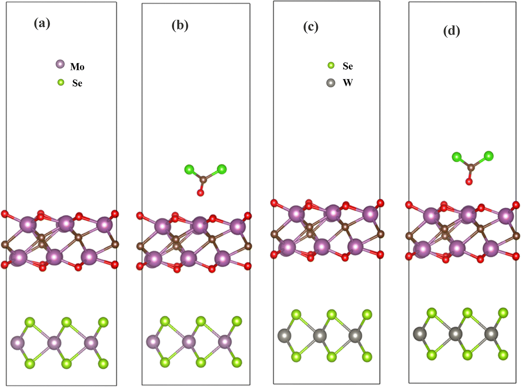
On perusal of improving the phosgene detection, we tried sensing based on heterostructures of Sc2CO2 and transition metal dichalcogenides (TMDs).76 When two semiconducting materials with different band gaps and distinct Fermi potentials are electrically connected, electrons flow from a higher energy state to a lower one until equilibrium is reached. This results in charge depletion near the interface region, creating a barrier potential due to band bending caused by the disparity in Fermi potentials between the respective materials. The critical requirement for enabling the sensing phenomenon involves the modulation of the barrier potential formed at the heterojunction interface.77,78 Among several TMDs, MoSe2 and WSe2 were chosen based on their lattice parameters and small lattice mismatch. The unit cells with lattice parameters 3.322 Å and 3.3199 Å were chosen for MoSe2 and WSe2, respectively. Moreover, the observed lattice mismatch of MoSe2/Sc2CO2 and WSe2/Sc2CO2 heterostructures was found to be 3.59% and 3.66%, respectively. The bandgaps of MoSe2 and WSe2 monolayers were reported to be close to 1.6 eV and 1.73 eV, respectively.79,80 MoSe2 is an inherent n-type semiconductor and WSe2 is a p-type semiconductor.81 A vacuum layer height of 21 Å was set in order to avoid interaction of other layers. The optimized heterostructures of MoSe2/Sc2CO2 and WSe2/Sc2CO are presented in Fig. 9(a) and (c).
 |
| | Fig. 9 (a) Sc2CO2_MoSe2 hetero-structure, (b) Sc2CO2_MoSe2 hetero-structure after phosgene interaction. (c) Sc2CO2_WSe2 hetero-structure. (d) Sc2CO2_WSe2 hetero-structure after phosgene interaction. | |
The distance between MoSe2 and Sc2CO2 in the heterojunction structure after optimization was found to be 3.8 Å, while the distance between the two layers was set at 4.46 Å initially. The distance between WSe2 and Sc2CO2 in the heterojunction structure after optimization was found to be 3.55 Å, while the distance between the two layers was set at 4 Å initially. The observed bond lengths of W–Se, Mo–Se, Sc–C, and Sc–O after the formation of heterostructures are presented in Table 4. No magnetic behaviour was observed in the heterostructures before and after the gas interaction. Moreover, the binding energy (Ebind) of the heterostructures was calculated to check the thermodynamic stability.43 The equation of binding energy is as follows:
| | | Ebind = ESc2CO2+TMD − ESc2CO2 − ETMD | (7) |
where
ESc2CO2+TMD,
ESc2CO2, and
ETMD are the total energies of the heterostructure, Sc
2CO, and TMD monolayers respectively. The obtained binding energies of MoSe
2/Sc
2CO
2 and WSe
2/Sc
2CO
2 are −0.666 eV and −0.603 eV, respectively.
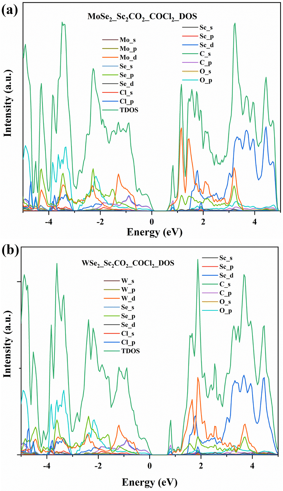
In order to understand the electronic properties, the density of states spectra of MoSe2/Sc2CO2 and WSe2/Sc2CO2 were calculated, and are shown in Fig. 10(a) and (b). It can be observed that the bandgaps of MoSe2/Sc2CO2 and WSe2/Sc2CO2 heterostructures are 0.65 eV and 0.88 eV, respectively. Moreover, it can be observed that the conduction band minimum is mainly composed of Mo-d orbitals and W-d orbitals for MoSe2- and WSe2-based heterostructures, respectively. Even, the electrical conductivity of both the heterostructures appears to be higher than that of the pristine Sc2CO2 monolayer.
 |
| | Fig. 10 (a) PDOS and TDOS of MoSe2 and Sc2CO2 heterostructures. (b) PDOS and TDOS of WSe2 and Sc2CO2 heterostructures. | |
3.3.2 Adsorption of COCl2 gas molecules.
The sensing mechanism of COCl2 on heterostructures was also examined based on the parameters mentioned in the previous section. The adsorption energies of COCl2 on MoSe2/Sc2CO2 and WSe2/Sc2CO2 were found to be −1.905 eV and −1.915 eV, respectively. Similar to pristine Sc2CO2, these structures succeeded in exhibiting strong adsorption. The adsorption energies of the van der Waals corrected structures were also calculated, and are reported in Table 2. The recovery time has shown ten times improvement, as shown in Table 2. The band gaps observed from the density of states spectra on MoSe2/Sc2CO2 and Wse2/Sc2CO2 are 0.5 eV and 0.6 eV, respectively. The significant change in the bandgap (Fig. 11(a)) is contributed by Mo-d, C-p, and Cl-p states near the conduction band minimum, whereas, in Wse2/Sc2CO2 (Fig. 11(b)), a slight deviation is observed. The bands near conduction band minimum are formed by Cl-p, O-p, and C-p states. This shows a great interaction of COCl2 on the Wse2/Sc2CO2 heterostructure as compared to the pristine Sc2CO2 monolayer and MoSe2/Sc2CO2 heterostructure. Additionally, the electrical conductivity in heterostructures was found to be more than four times that of the Sc2CO2 monolayer.
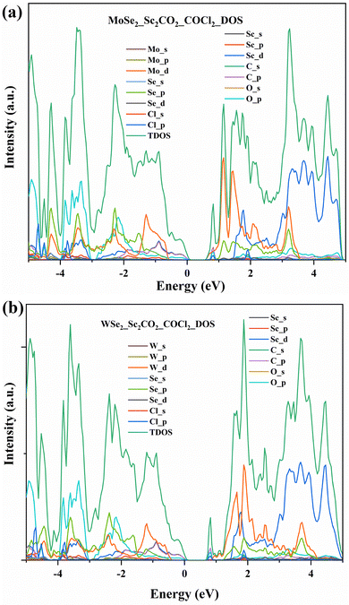 |
| | Fig. 11 (a) PDOS and TDOS of MoSe2 and Sc2CO2 heterostructures after interaction with COCl2. (b) PDOS and TDOS of WSe2 and Sc2CO2 heterostructures after interaction with COCl2. | |
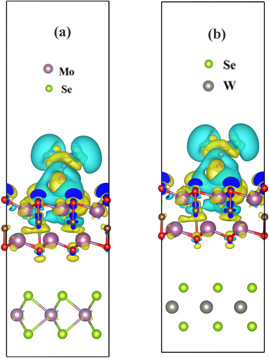
With the aim to verify the interaction further, we also calculated the charge transfer from the Bader charge analysis. The charge transfer in MoSe2/Sc2CO2 and WSe2/Sc2CO2 from COCl2 was found to be 1.867e− and 1.880e−, respectively. Moreover, the charge density difference on heterostructures after interaction with COCl2 is visualised in Fig. 12. It can be observed that there is a significant charge redistribution upon the formation of TMD/MXene heterostructures (Fig. 12), as compared to the pristine Sc2CO2 monolayer (Fig. 8e). This shows a clear improvement in the interaction of COCl2 on the receptor layer due to the formation of heterostructures. From the CDD plot of MoSe2/Sc2CO2 (Fig. 12(a)), a small amount of charge accumulation and depletion can be seen in the Mo atom of the MoSe2 layer. On the contrary, no interaction can be seen in the WSe2 layer of the WSe2/Sc2CO2 heterostructure. This suggests the higher interaction of MoSe2 over WSe2.
 |
| | Fig. 12 Charge density difference of (a) Sc2CO2_MoSe2 hetero-structure and (b) Sc2CO2_WSe2 hetero-structure, after interaction with COCl2. The isosurface value is set at 0.0001 e bohr−3. | |
4. Conclusions
In conclusion, Sc2CO2 MXenes demonstrate considerable promise for phosgene gas sensing based on density functional theory calculations. This analysis reveals that pristine Sc2CO2 exhibits semiconducting behavior, indicating its potential as a semiconductor gas sensor. The analysis based on adsorption energies reveals a notably strong affinity of Sc2CO2 MXenes towards phosgene. As the MXene surface is likely to become predominantly covered by O2 and N2 when exposed to air, potentially impacting the sensor function, their effects were analysed. The very low adsorption of O2 and N2 molecules suggests the selective detection of COCl2. Notably, the formation of MoSe2 and WSe2 heterostructures exhibited improvement in sensing parameters. To address the challenges associated with crucial factors in gas sensing such as recovery time between adsorption and desorption, this study proposes strategies involving high operational temperatures and the formation of heterostructures with transition metal dichalcogenides. Thus, these approaches are anticipated to enhance both recovery times and electrical conductivity, thereby improving the overall sensor performance. Future investigations could explore the estimation of sensing capabilities through current–voltage (I–V) characteristic calculations both theoretically and experimentally. Such analyses would offer deeper insights into the electrical response of Sc2CO2 MXenes to gas molecules, facilitating optimization and advancement towards robust gas sensing applications.
Author contributions
Julaiba T. Mazumder: conceptualization, software, formal analysis, writing – original draft. Mohammed M. Hasan: software, formal analysis, writing – review & editing. Fahim Parvez: software, data collection, Tushar Shivam: drawing and plotting, Dobbidi Pamu: writing – review & editing. Alamgir Kabir: resources, writing – review & editing. Mainul Hossain: supervision, writing – review & editing. Ravindra K. Jha: conceptualization, resources, writing – review & editing, supervision.
Data availability
Complete data will be made available upon request. However, ESI,† is included along with the manuscript.
Conflicts of interest
There are no conflicts to declare.
Acknowledgements
The authors express gratitude to the members of the Nano Sensors and Devices lab. JTM acknowledges the institute post-doctoral fellowship from the R&D Section at IIT Guwahati. RKJ acknowledges funding support from the Department of Science and Technology (DST) under grant no.: DST/TDT/TDP-46/2022 and from the IIT Guwahati Technology Innovation and Development Foundation (TIDF) under grant no.: TIH/TD/0115. All authors appreciate the support from the Department of Electronics and Electrical Engineering (EEE), the Centre for Intelligent Cyber-Physical Systems (CICPS) at IIT Guwahati, and the Computational Material Science Lab at the University of Dhaka, Bangladesh. The authors also acknowledge the technical support received from Rishikanta Mayengbam, Nanyang Technological University Singapore.
References
-
M. A. Von Zimmerman and T. C. Arnold, Phosgene toxicity, StatPearls, Dec. 2022, StatPearls Publishing, Treasure Island (FL), 2024, https://www.ncbi.nlm.nih.gov/books/NBK589660/ Search PubMed.
- K. Ganesan, S. K. Raza and R. Vijayaraghavan, Chemical warfare agents, J. Pharm. BioAllied Sci., 2010, 2(3), 166, DOI:10.4103/0975-7406.68498.
- S. A. Cucinell, E. Arsenal and S. A. Cucinell, Review of the toxicity of long-term phosgene exposure, Arch. Environ. Health, 1974, 28(5), 272–275, DOI:10.1080/00039896.1974.10666485.
- A. K. Vaish,
et al., Accidental phosgene gas exposure: a review with background study of 10 cases, J. Emerg. Trauma. Shock, 2013, 6(4), 271, DOI:10.4103/0974-2700.120372.
- D. Feng, Y. Zhang, W. Shi, X. Li and H. Ma, A simple and sensitive method for visual detection of phosgene based on the aggregation of gold nanoparticles, Chem. Commun., 2010, 46(48), 9203–9205, 10.1039/C0CC02703K.
- K. Cheng, N. Yang, Q. Y. Li, X. W. Gao and X. J. Wang, Selectively light-up detection of phosgene with an aggregation-induced emission-based fluorescent sensor, ACS Omega, 2019, 4(27), 22557–22561, DOI:10.1021/ACSOMEGA.9B03286.
- Y. Zhang,
et al., An effective fluorescent probe for detection of phosgene based on naphthalimide dyes in liquid and gaseous phases, Spectrochim. Acta, Part A, 2023, 289, 122189, DOI:10.1016/J.SAA.2022.122189.
- A. B. Solea, C. Curty, K. M. Fromm, C. Allemann and O. Mamula Steiner, A Rapid, Highly sensitive and selective phosgene sensor based on 5,6-pinenepyridine, Chem. – Eur. J., 2022, 28(55), e202201772, DOI:10.1002/CHEM.202201772.
- F. Zeng, G. Bao, B. Zhou and Y. Han, A new fluorescent probe for ultrasensitive detection of phosgene in solution and the gas phase, New J. Chem., 2021, 45(12), 5631–5636, 10.1039/D1NJ00037C.
- Z. Chang,
et al., Adsorption, sensing, electronic and magnetic properties of phosgene (COCl2) molecule adsorbed on Nb-doped arsenene: first-principles study, Solid State Commun., 2022, 357, 114975, DOI:10.1016/J.SSC.2022.114975.
- Y. Gogotsi and Q. Huang, MXenes: two-dimensional building blocks for future materials and devices, ACS Nano, 2021, 15(4), 5775–5780, DOI:10.1021/acsnano.1c03161.
- Y. Wang, Y. Wang, Y. Kuai and M. Jian, “Visualization” gas–gas sensors based on high performance novel MXenes materials, Small, 2024, 20(2), 2305250, DOI:10.1002/SMLL.202305250.
- S. J. Kim,
et al., Metallic Ti3C2Tx MXene gas sensors with ultrahigh signal-to-noise ratio, ACS Nano, 2018, 12(2), 986–993, DOI:10.1021/ACSNANO.7B07460.
- H. F. Zhang,
et al., Strategies and challenges for enhancing performance of MXene-based gas sensors: a review, Rare Met., 2022, 41(12), 3976–3999, DOI:10.1007/S12598-022-02087-X.
- J. Lee, E. Yang and S. J. Kim, Gas-sensing properties and applications of MXenes, MRS Bull., 2023, 48(3), 261–270, DOI:10.1557/S43577-023-00495-7/METRICS.
- S. Atkare, C. S. Rout and S. Jagtap, Perspectives of 2D MXene-based materials for self-powered smart gas sensors, Mater. Adv., 2024, 5(4), 1440–1453, 10.1039/D3MA00890H.
- S. Thomas and M. Asle Zaeem, Phosgene gas sensing of Ti2CT2 (T = F−, O−, OH−) MXenes, Adv. Theory Simul., 2021, 4(3), 2000250, DOI:10.1002/ADTS.202000250.
- P. Panigrahi, Y. Pal, T. Kaewmaraya, H. Bae, N. Nasiri and T. Hussain, Molybdenum carbide MXenes as efficient nanosensors toward selected chemical warfare agents, ACS Appl. Nano Mater., 2023, 6(10), 8404–8415, DOI:10.1021/ACSANM.3C00686/.
- H. Xiong, B. Liu, H. Zhang and J. Qin, Theoretical insight into two-dimensional M-Pc monolayer as an excellent material for formaldehyde and phosgene sensing, Appl. Surf. Sci., 2021, 543, 148805, DOI:10.1016/J.APSUSC.2020.148805.
- D. Yang, X. Fan, D. Zhao, Y. An, Y. Hu and Z. Luo, Sc2CO2 and Mn-doped Sc2CO2 as gas sensor materials to NO and CO: a first-principles study, Phys. E, 2019, 111, 84–90, DOI:10.1016/J.PHYSE.2019.02.019.
- Y. Lee, Y. Hwang, S. B. Cho and Y. C. Chung, Achieving a direct band gap in oxygen functionalized-monolayer scandium carbide by applying an electric field, Phys. Chem. Chem. Phys., 2014, 16(47), 26273–26278, 10.1039/C4CP03811H.
- Q. Chen, D. Zhang, J. Pan and W. Fan, Optical properties of two-dimensional semi-conductive MXene Sc2COx produced by sputtering, Optik, 2020, 219, 165046, DOI:10.1016/J.IJLEO.2020.165046.
- Y. Wang, Y. Wang, M. Jian, Q. Jiang and X. Li, MXene key composites: a new arena for gas sensors, Nanomicro Lett., 2024, 16(1), 1–42, DOI:10.1007/S40820-024-01430-4.
- M. J. Szary, Computational study of the intercalation of NO2 between bilayer MoTe2, Appl. Surf. Sci., 2023, 611, 155514, DOI:10.1016/j.apsusc.2022.155514.
- A. Bag and N. E. Lee, Gas sensing with heterostructures based on two-dimensional nanostructured materials: a review, J. Mater. Chem. C, 2019, 7(43), 13367–13383, 10.1039/C9TC04132J.
- R. K. Jha, J. V. D’Costa, N. Sakhuja and N. Bhat, MoSe2 nanoflakes based chemiresistive sensors for ppb-level hydrogen sulfide gas detection, Sens. Actuators, B, 2019, 297, 126687, DOI:10.1016/J.SNB.2019.126687.
- D. Kumar, R. Kumar and R. Chaurasiya, Janus HfSSe monolayer: a promising candidate for SO2 and COCl2 gas sensing, Nanotechnology, 2024, 35(19), 195501, DOI:10.1088/1361-6528/AD2383.
- W. Y. Chen, X. Jiang, S. N. Lai, D. Peroulis and L. Stanciu, Nanohybrids of a MXene and transition metal dichalcogenide for selective detection of volatile organic compounds, Nat. Commun., 2020, 11(1), 1–10, DOI:10.1038/s41467-020-15092-4.
- S. Aftab,
et al., New developments in gas sensing using various two-dimensional architectural designs, Chem. Eng. J., 2023, 469, 144039, DOI:10.1016/J.CEJ.2023.144039.
- H. Yan, L. Chu, Z. Li, C. Sun, Y. Shi and J. Ma, 2H-MoS2/Ti3C2Tx MXene composites for enhanced NO2 gas sensing properties at room temperature, Sens. Actuators, Rep., 2022, 4, 100103, DOI:10.1016/J.SNR.2022.100103.
- L. Wu, C. Dong, C. Chen, L. Zhao, P. Lu and K. Yang, Interface engineering at Sc2C MXene and germanium iodine perovskite interface: first-principles insights, J. Phys. Chem. Lett., 2022, 13(50), 11801–11810, DOI:10.1021/ACS.JPCLETT.2C03478.
- L. Li and W. Shi, Tuning electronic structures of Sc2CO2/MoS2 polar–nonpolar van der Waals heterojunctions: interplay of internal and external electric fields, J. Mater. Chem. C, 2017, 5(32), 8128–8134, 10.1039/C7TC02384G.
- H. L. Hou, C. Anichini, P. Samorì, A. Criado and M. Prato, 2D van der Waals heterostructures for chemical sensing, Adv. Funct. Mater., 2022, 32(49), 2207065, DOI:10.1002/ADFM.202207065.
- T. He, S. Sun, B. Huang and X. Li, MXene/SnS2 heterojunction for detecting sub-ppm NH3 at room temperature, ACS Appl. Mater. Interfaces, 2023, 15(3), 4194–4207 CrossRef CAS PubMed.
- R. K. Jha, A. Nanda, A. Yadav, R. Sai and N. Bhat, 2D-MoSe2/0D-ZnO nanocomposite for improved H2S gas sensing in dry air ambience, J. Alloys Compd., 2022, 926, 166825, DOI:10.1016/J.JALLCOM.2022.166825.
- D. Raval, S. K. Gupta and P. N. Gajjar, Detection of H2S, HF and H2 pollutant gases on the surface of penta-PdAs2 monolayer using DFT approach, Sci. Rep., 2023, 13(1), 1–10, DOI:10.1038/s41598-023-27563-x.
- U. Yorulmaz, A. Özden, N. K. Perkgöz, F. Ay and C. Sevik, Vibrational and mechanical properties of single layer MXene structures: a first-principles investigation, Nanotechnology, 2016, 27(33), 335702, DOI:10.1088/0957-4484/27/33/335702.
- F. Opoku, S. O. B. Oppong, A. Aniagyei, O. Akoto and A. A. Adimado, Boosting the photocatalytic H2 evolution activity of type-II g-GaN/Sc2 CO2 van der Waals heterostructure using applied biaxial strain and external electric field, RSC Adv., 2022, 12(12), 7391–7402, 10.1039/D2RA00419D.
- G. Kresse and J. Hafner, Ab initio molecular-dynamics simulation of the liquid–metal–amorphous–semiconductor transition in germanium., Phys. Rev. B: Condens. Matter Mater. Phys., 1994, 49, 14251, DOI:10.1103/PhysRevB.49.14251.
- K. Momma and F. Izumi, VESTA: a three-dimensional visualization system for electronic and structural analysis, J. Appl. Crystallogr., 2008, 41(3), 653–658, DOI:10.1107/S0021889808012016.
- L. S. Pedroza, A. J. R. Da Silva and K. Capelle, Gradient-dependent density functionals of the Perdew–Burke–Ernzerhof type for atoms, molecules, and solids, Phys. Rev. B: Condens. Matter Mater. Phys., 2009, 79(20), 201106, DOI:10.1103/PhysRevB.79.201106.
- J. T. Mazumder and R. K. Jha, Theoretical insights into gas sensing properties of MXene, Sens. Actuators, Rep., 2023, 100174, DOI:10.1016/j.snr.2023.100174.
- S. Bae, Y. G. Kang, M. Khazaei, K. Ohno, Y. H. Kim, M. J. Han, K. J. Chang and H. Raebiger, Electronic and magnetic properties of carbide MXenes—the role of electron correlations, Mater. Today Adv., 2021, 9, 100118, DOI:10.1016/j.mtadv.2020.100118.
- T. He, S. Sun, B. Huang and X. Li, MXene/SnS2 heterojunction for detecting sub-ppm NH3 at room temperature, ACS Appl. Mater. Interfaces, 2023, 15(3), 4194–4207, DOI:10.1021/acsami.2c18097.
- F. Assareh Pour, G. Darvish and R. Faez, Interfacial and electrical properties of Si/APS/MAPbI3 heterostructure: an ab initio study, J. Phys. Chem. C, 2025, 129(8), 4172–4182, DOI:10.1021/acs.jpcc.4c07083.
- M. J. Szary, Toward high selectivity of sensor arrays: enhanced adsorption interaction and selectivity of gas detection (N2, O2, NO, CO, CO2, NO2, SO2, AlH3, NH3, and PH3) on transition metal dichalcogenides (MoS2, MoSe2, and MoTe2), Acta Mater., 2024, 274, 120016, DOI:10.1016/j.actamat.2024.120016.
- M. Birowska, K. Milowska and J. A. Majewski, Van der Waals density functionals for graphene layers and graphite, Acta Phys. Pol., A, 2011, 120(5), 845–848, DOI:10.12693/APhysPolA.120.845.
- H. Guo, B. Zhu, F. Zhang, H. Li, K. Zheng, J. Qiu, L. Wu, J. Yu and X. Chen, Type-II AsP/Sc2CO2 van der Waals heterostructure: an excellent photocatalyst for overall water splitting, Int. J. Hydrogen Energy, 2021, 46(65), 32882–32892, DOI:10.1016/j.ijhydene.2021.07.125.
- T. Tian, X. Zhou, J. Yu, J. Bai, L. Chen, N. He, X. Li, H. Zhang and H. Cui, First-principles predictions of MoS2-WS2 in-plane heterostructures for sensing dissolved gas species in oil-immersed transformers, ACS Omega, 2024, 9(18), 20253–20262, DOI:10.1021/acsomega.4c00681.
- P. Giannozzi,
et al., Quantum espresso: a modular and open-source software project for quantum simulations of materials, J. Phys.: Condens. Matter, 2009, 21, 395502, DOI:10.1088/0953-8984/21/39/395502.
- Z. Wang,
et al., First-principles study of electronic and optical properties of NH3-adsorbed Sc2CO2 monolayer and its application in gas sensors, J. Mater. Res. Technol., 2023, 24, 173–184, DOI:10.1016/J.JMRT.2023.02.211.
- A. A. Banu, S. Sinthika, S. Premkumar, J. Vigneshwaran, S. Z. Karazhanov and S. P. Jose, DFT study of NH3 adsorption on 2D monolayer MXenes (M2C, M = Cr, Fe) via oxygen functionalization: suitable materials for gas sensors, FlatChem, 2022, 31, 100329, DOI:10.1016/j.flatc.2021.100329.
- F. Nejadsattari and Z. M. Stadnik, Spin polarized density functional theory calculations of the electronic structure and magnetism of the 112 type iron pnictide compound EuFeAs2, Sci. Rep., 2021, 11(1), 1–15, DOI:10.1038/s41598-021-91301-4.
- V. Wang, N. Xu, J. C. Liu, G. Tang and W. T. Geng, VASPKIT: a user-friendly interface facilitating high-throughput computing and analysis using VASP code, Comput. Phys. Commun., 2021, 267, 108033, DOI:10.1016/J.CPC.2021.108033.
- M. N. Gjerding, M. Pandey and K. S. Thygesen, Band structure engineered layered metals for low-loss plasmonics, Nat. Commun., 2017, 8(1), 1–8, DOI:10.1038/ncomms15133.
- J. Bekaert, R. Saniz, B. Partoens and D. Lamoen, Native point defects in CuIn1−xGaxSe2: hybrid density functional calculations predict the origin of p- and n-type conductivity, Phys. Chem. Chem. Phys., 2014, 16(40), 22299–22308, 10.1039/C4CP02870H.
- J. Guo, Y. Sun, B. Liu, Q. Zhang and Q. Peng, Two-dimensional scandium-based carbides (MXene): band gap modulation and optical properties, J. Alloys Compd., 2017, 712, 752–759, DOI:10.1016/J.JALLCOM.2017.04.149.
- K. H. Habura, M. A. Afrassa and F. G. Hone, Density functional theory study of Zn(1−x)FexSe: electronic structure, phonon, and magnetic properties, AIP Adv., 2023, 13, 035102, DOI:10.1063/5.0133408/2880644.
- A. H. Ati,
et al., Computational study of half-metallic behavior, optoelectronic and thermoelectric properties of new XAlN3 (X = K, Rb, Cs) perovskite materials, J. Phys. Chem. Solids, 2024, 188, 111899, DOI:10.1016/J.JPCS.2024.111899.
- G. M. Mustafa, Z. Ullah, M. A. Ameer, N. A. Noor, S. Mumtaz and M. K. Al-Sadoon, Exploring half-metallic ferromagnetism and thermoelectric properties of Tl2WX6 (X = Cl and Br) double perovskites, RSC Adv., 2024, 14(26), 18385–18394, 10.1039/D4RA02465F.
- K. Cheng,
et al., Monolayer Sc2CF2 as a potential selective and sensitive NO2 sensor: insight from first-principles calculations, ACS Omega, 2022, 7(11), 9267–9275, DOI:10.1021/ACSOMEGA.1C06027.
- S. Xu, H. Zhao, Y. Xu, R. Xu and Y. Lei, Carrier mobility-dominated gas sensing: a room-temperature gas-sensing mode for SnO2 nanorod array sensors, ACS Appl. Mater. Interfaces, 2018, 10(16), 13895–13902, DOI:10.1021/ACSAMI.8B03953.
- M. Ziati, N. Bekkioui and H. Ez-Zahraouy, Correlation between carrier mobility and effective mass in Sr2RuO4−xFx (x = 2) under uniaxial strain using the Yukawa screened PBE0 hybrid functional, J. Phys. Chem. Solids, 2022, 161, 110409, DOI:10.1016/j.jpcs.2021.110409.
- M. A. Franco, P. P. Conti, R. S. Andre and D. S. Correa, A review on chemiresistive ZnO gas sensors, Sens. Actuators, Rep., 2022, 4, 100100, DOI:10.1016/J.SNR.2022.100100.
- N. Goel, K. Kunal, A. Kushwaha and M. Kumar, Metal oxide semiconductors for gas sensing, Eng. Rep., 2023, 5(6), e12604, DOI:10.1002/ENG2.12604.
- J. Gagné, J. K. Faherty, K. L. Cruz, Y. O. Ciftci and B. Çatıkkaş, Pressure effects on the structural, electronic, elastic, optical, and vibrational properties of YMg intermetallic compounds: a first-principles study, Phys. Scr., 2024, 99(6), 065981, DOI:10.1088/1402-4896/AD48E6.
- C. Rong,
et al., Elastic properties and tensile strength of 2D Ti3C2Tx MXene monolayers, Nat. Commun., 2024, 15(1), 1–8, DOI:10.1038/s41467-024-45657-6.
- J. R. Fragoso-Mora,
et al., Gas sensors based on elasticity changes of nanoparticle layers, Sens. Actuators, B, 2018, 268, 93–99, DOI:10.1016/J.SNB.2018.04.045.
- J. T. Mazumder, R. Mayengbam and S. K. Tripathy, Theoretical investigation on structural, electronic, optical and elastic properties of TiO2, SnO2, ZrO2 and
HfO2 using SCAN meta-GGA functional: a DFT study, Mater. Chem. Phys., 2020, 254, 123474, DOI:10.1016/J.MATCHEMPHYS.2020.123474.
- F. Mouhat and F. X. Coudert, Necessary and sufficient elastic stability conditions in various crystal systems, Phys. Rev. B: Condens. Matter Mater. Phys., 2014, 90, 224104, DOI:10.1103/PhysRevB.90.224104.
- A. Chaves,
et al., Bandgap engineering of two-dimensional semiconductor materials, npj 2D Mater. Appl., 2020, 4(1), 1–21, DOI:10.1038/s41699-020-00162-4.
- S. Wu, W. P. C. Lee and P. Wu, Origin of observed narrow bandgap of mica nanosheets, Sci. Rep., 2022, 12(1), 1–11, DOI:10.1038/s41598-022-06820-5.
- D. Bahamon, M. Khalil, A. Belabbes, Y. Alwahedi, L. F. Vega and K. Polychronopoulou, A DFT study of the adsorption energy and electronic interactions of the SO2 molecule on a CoP hydrotreating catalyst, RSC Adv., 2021, 11(5), 2947–2957, 10.1039/C9RA10634K.
- A. Bano, J. Krishna, T. Maitra and N. K. Gaur, CrI3-WTe2: a Novel two-dimensional heterostructure as multisensor for BrF3 and COCl2 toxic gases, Sci. Rep., 2019, 9(1), 1–8, DOI:10.1038/s41598-019-47685-5.
- M. Yuan,
et al., Electrochemical C–N coupling with perovskite hybrids toward efficient urea synthesis, Chem. Sci., 2021, 12(17), 6048, 10.1039/D1SC01467F.
- S. Yang, C. Jiang and S. Huai Wei, Gas sensing in 2D materials, Appl. Phys. Rev., 2017, 4, 021304, DOI:10.1063/1.4983310/279723.
- F. Ashraf Ali, D. Kumar Mishra, R. Nayak and B. Nanda, Solid-state gas sensors: sensing mechanisms and materials, Bull. Mater. Sci., 2022, 45(15) DOI:10.1007/s12034-021-02581-5.
- B. Cho,
et al., Chemical Sensing of 2D Graphene/MoS2 Heterostructure device, ACS Appl. Mater. Interfaces, 2015, 7(30), 16775–16780, DOI:10.1021/ACSAMI.5B04541.
- S. Deng, L. Li and M. Li, Stability of direct band gap under mechanical strains for monolayer MoS2, MoSe2, WS2 and WSe2, Phys. E, 2018, 101, 44–49, DOI:10.1016/J.PHYSE.2018.03.016.
- C. Xia Yang, X. Zhao and S. Yi Wei, Manipulation of electronic structure in WSe2 monolayer by strain, Solid State Commun., 2016, 245, 70–74, DOI:10.1016/J.SSC.2016.07.003.
- X. Li,
et al., Isoelectronic Tungsten Doping in Monolayer MoSe2 for Carrier Type Modulation, Adv. Mater., 2016, 28(37) DOI:10.1002/adma.201601991.
|
| This journal is © the Owner Societies 2025 |
Click here to see how this site uses Cookies. View our privacy policy here. 
 Open Access Article
 This Open Access Article is licensed under a Creative Commons Attribution-Non Commercial 3.0 Unported Licence
 e,
Tushar
Shivam
a,
Dobbidi
Pamu
f,
Alamgir
Kabir
e,
Tushar
Shivam
a,
Dobbidi
Pamu
f,
Alamgir
Kabir