
 Open Access Article
 This Open Access Article is licensed under a Creative Commons Attribution-Non Commercial 3.0 Unported Licence
Quantitative modeling of point defects in β-Ga2O3 combining hybrid functional energetics with semiconductor and processes thermodynamics†
K. A.
Arnab
 a,
M.
Stephens
a,
I.
Maxfield
a,
C.
Lee
bc,
E.
Ertekin
bcd,
Y. K.
Frodason
e,
J. B.
Varley
f and
M. A.
Scarpulla
*ag
a,
M.
Stephens
a,
I.
Maxfield
a,
C.
Lee
bc,
E.
Ertekin
bcd,
Y. K.
Frodason
e,
J. B.
Varley
f and
M. A.
Scarpulla
*ag
aDepartment of Materials Science and Engineering, University of Utah, Salt Lake City, Utah 84112, USA. E-mail: mike.scarpulla@utah.edu
bDepartment of Mechanical Science and Engineering, University of Illinois at Urbana-Champaign, Urbana, Illinois 61801, USA
cThe Grainger College of Engineering, University of Illinois Urbana-Champaign, Urbana, Illinois 61801, USA
dMaterials Research Laboratory, University of Illinois at Urbana-Champaign, Urbana, Illinois 61801, USA
eCentre for Materials Science and Nanotechnology Physics, University of Oslo, Oslo, Norway
fLawrence Livermore National Laboratory, Livermore, California 93106, USA
gDepartment of Electrical and Computer Engineering, University of Utah, Salt Lake City, Utah 84112, USA
First published on 16th May 2025
Abstract
β-Gallium oxide (β-Ga2O3) is of high interest for power electronics because of its unique combination of melt growth, epitaxial growth, n-type dopability, ultrawide bandgap, and high critical field. Optimization of crystal growth processes to promote beneficial defects and suppress harmful ones requires accurate quantitative modelling of both native and impurity defects. Herein we quantitatively model defect concentrations as a function of bulk crystal growth conditions and demonstrate the necessity of including effects such as bandgap temperature dependence, chemical potentials from thermochemistry, and defect vibrational entropy in modelling based on defect formation energies computed by density functional theory (DFT) with hybrid functionals. Without these contributions, grossly-erroneous and misleading predictions arise, e.g. that n-type doping attempts would be fully compensated by Ga vacancies. Including these effects reproduces the experimental facts that melt-grown Sn-doped β-Ga2O3 crystals are conductive with small compensation while annealing the same crystals in O2 at intermediate temperatures renders them insulating. To accomplish this modeling, we developed a comprehensive modelling framework (KROGER) based on calculated defect formation energies and flexible thermodynamic conditions. These capabilities allow KROGER to capture full and partial defect equilibria amongst native defects and impurities occurring during specific semiconductor growth or fabrication processes. We use KROGER to model 873 charge-states of 259 defects involving 19 elements in conditions representing bulk crystal growth by edge-fed growth (EFG) and annealing in oxygen. Our methodology is transferrable to a wide range of materials beyond β-Ga2O3. The integration of thermodynamic and first-principles modelling of point defects provides insight into optimization of point defect populations in growth and processing.
Introduction
β-Gallium oxide (β-Ga2O3) is of intense current interest for power electronics because of its ultra-wide bandgap, high critical field, controllable n-type doping, and the availability of native melt-grown substrates.1–3 The properties of bulk single crystals and epitaxial layers are intimately tied to point defects and complexes, necessitating predictive models for defect concentrations resulting from varying impurities and processing histories. While density functional theory (DFT) calculations have offered critical qualitative insights into prevalent defects based on calculated formation energies4–11 translating these findings to actual concentrations of defects present for specific real-world crystal growth and processing requires incorporation of multiple temperature, atmosphere and pressure dependent factors. For example and as we will detail below, a typical calculation holding DFT-calculated formation energies of native and Sn-related defects constant versus temperature predicts that Sn-doped crystals grown at Tmelt = 2068 °C by edge-fed growth (EFG) with pO2 = 0.02 atm should yield crystals fully-compensated by gallium vacancies (VGa) and related complexes (SnGa–VGa, VGa–VO, etc.). Yet Sn-doped wafers can be purchased commercially and in actuality display (nearly) degenerate n-type doping with <1% compensation.12,13 The accuracy of DFT-based defect modelling of charge transition levels compared to experiments brought by large supercells with finite-size correction schemes, hybrid functionals and self-interaction corrections usher in a new era in defect modelling in which it is worth the effort to incorporate the aforementioned thermodynamic effects.14,15 The case study of systematically incorporating a suite of thermodynamic contributions for β-Ga2O3 herein sets a benchmark for achieving quantitative agreement with experiments by combining all of these factors.16,17Here we utilize a comprehensive, transferrable, quantitative framework dubbed KROGER18 for modelling full, partial, and constrained defect equilibria to emulate defects resulting from real-world growth and processing.19 KROGER,18 named after F. A. Kroger who gave exhaustive treatments of point defect concentrations,20,21 allows us to take a set of DFT-computed formation energies for the charge states of defects and complexes and compute their numbers given specified thermodynamic conditions representing real-world processing.14 β-Ga2O3 is used as an exemplar and through this modelling we elucidate new insights specific to this material's defect chemistry, but of course the methodology is transferrable to other materials. We account for the temperature dependencies of the bandgap and densities of states, temperature- and pressure-dependent chemical potentials from the Ga–O binary system, degenerate statistics, self-trapped holes (STHs), and a minimal quantum harmonic oscillator model for vibrational entropy change for defects which can exceed 1.5 eV per defect near Tmelt. We model EFG-grown unintentionally-doped (UID), Sn-, Fe- and Mg-doped crystals by calculating defect equilibrium based on their reported total dopant and impurity concentrations rather than assuming fixed chemical potentials. We illustrate how assuming kinetic trapping of dopants in combination with the aforementioned temperature dependencies yields agreement with experiments. The ability to model various constrained equilibria gives KROGER added capabilities for modelling semiconductor processing beyond the state of the art.22–29
We illustrate the scalability of our modelling framework and ability to explicitly handle trace impurities by including a total of 19 elements distributed across 259 defects having 873 charge states, as well as self-trapped holes localized on OI and OII atoms;30,31 limited only by the availability of a self-consistent set of DFT-calculated formation energies for all these defects’ charge states. Such calculations at dozens of temperatures run within minutes on a personal computer, allowing rapid exploration of various effects. We accurately model defects in Sn, Fe, and Mg-doped edge-fed growth (EFG) crystals, Bridgeman crystals grown under different pO2, and annealing experiments in pure O2 at 1 atm. We compare our results with the well-established parameters of Sn-doped Ga2O3, such as the electron and donor concentration ratio and DLOS data on VGa-related defect densities.32 This work provides novel insights into defects and complexes in β-Ga2O3 while also illustrating the capabilities of KROGER which was built for generality and transferability to defect systems in other materials. This comprehensive approach yields insights beyond those typically possible from DFT defect formation energetics evaluated in certain rich and poor chemical potential conditions.
Results & discussion
Establishing a baseline model for defects in donor-doped EFG β-Ga2O3
In this paper, we primarily focus on the EFG method,33 as the properties of commercial wafers grown by this method are consistent and well-characterized. We also provide some results in the ESI† for Bridgman34 processes which utilize different noble metal crucibles. Both EFG and Bridgman growth of β-Ga2O3 utilize 1 atm total pressure, with EFG using 2% oxygen pO2 and Bridgman 20% pO2.35,36 All of the melt-growth techniques occur at Tm = 2068 K, and despite the different pO2 values converge on very close predictions because for gasses, chemical potential depends logarithmically on pressure. Additionally, we have carried out annealing experiments on 500–700 µm thick Sn-doped wafers in 1 atm pO2 at 1300–1400 K for durations up to 2 weeks, which was the time required for elimination of free carrier absorption.Fig. 1 illustrates three different models of temperature-dependent defect concentrations for EFG-grown Sn-doped β-Ga2O3 resulting from different assumptions about chemical potentials and impurity concentrations. To simplify plots, we have grouped similar defects and complexes, as discussed in the ESI.†Fig. 1(a) corresponds to kinetic trapping of [Sn] = 4.5 × 1018 cm−3, [Si] = 2 × 1017 cm−3 and [Fe] = 7 × 1016 cm−3 and O and Ga chemical potentials fixed by eqn (2) and (7) (see in Computational Methods) with pO2 = 0.02 atm. Subfigure (b) presents results assuming the O and Ga chemical potentials do not vary with temperature for O-rich conditions, in other words for the “O-rich” conditions presented in Varley et al.8–10 and Frodason et al.4–6 Part (c) is the same as (a) but with ΔμSn set by equilibrium with SnO2 using measured thermochemical data. The different temperature dependencies of ΔμGa, ΔμO, and ΔμSn for these cases are plotted in Fig. 2. In Fig. 1(a) and (c), the total concentrations of other impurities are fixed at representative values from Kuramata et al.33 In (a) and (c) the temperature dependence of bandgap is taken from Lee et al.37 with a representative assumption of 40% of ΔEg(T) occurring in the conduction band, as discussed in depth below in the context of Fig. 4. While not shown here, it is rather a simple task to combine models like (a) and (c) to make models accounting for dopant equilibration with 2nd phases at high temperatures but freezing in at some intermediate temperature.
 | ||
| Fig. 1 Defect concentrations calculated for Sn-doped β-Ga2O3 in different scenarios. (a) Fixed concentrations of Sn and other impurities and incorporating the full set of temperature-dependent effects for pO2 = 0.02 atm used in EFG growth.33 Both equilibrium and quenching scenarios are consistent with Sn-doped wafers being n-type with <1% compensation as long as the native defect system freezes-in by ∼1950 K. Overlap of equilibrium and quenched results predicts insensitivity to cooling rate. (b) “O-rich, Sn-doped” conditions38 without any temperature dependencies predicting that Sn-doped wafers should be insulating with >99% compensation (n in the 1015 range) for all temperatures, which disagrees with reality. (c) Similar to (a) in terms of other impurities but with μSn(T) set by equilibrium with SnO2. In this scenario, agreement with real EFG Sn-doped crystals could occur only if the native defect system and [Sn] simultaneously freeze-in at ∼1850 K, which would be more likely for larger crystals. This would be expected to depend sensitively on cooling rate, which is improbable given the widely-reported ease of reliable, low compensation bulk doping with Sn. Note that (c) represents the temperature-dependent solubility limit for Sn in β-Ga2O3 from thermochemistry; the fact that [Sn] > 1018 cm−3 is achievable without SnO2 precipitation is direct evidence for kinetic trapping of Sn. Note, [Si] was omitted in (c) to allow Sn to be the dominant donor for all temperatures and that the equilibrium solubility becomes dependent on the residual [MgGa] + [CaGa] − [ZrGa] at low temperatures. | ||
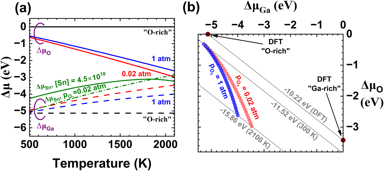 | ||
| Fig. 2 (a) Temperature dependent chemical potentials for Ga, O and Sn under different thermodynamic scenarios with ΔμO solid and ΔμGa dashed: typical O- or Ga-rich (black), based on thermochemical functions from the Ga–O system for pO2 = 0.02 and 1 atm (red, blue). For Sn (green), solid denotes the case where the total [Sn] is fixed while dash-dot is derived from the SnO2 phase boundary for pO2 = 0.02 atm. (b) Plot of ΔμGa and ΔμO in Ga–O chemical potential space. At 0 or 300 K, the experimental ΔHF = ΔG° (grey diagonal lines) is within 15% of the DFT-calculated value, but as Tm is approached this error increases to 50% and the locus of conditions for which pO2 is held constant moves quite far from either O-rich or Ga-rich conditions (blue or red circles). This illustrates why using chemical potentials from thermochemistry gives a more realistic prediction for defects present. | ||
We conclude that the model in (a) is the most likely to represent real-world crystals because it agrees with the physical expectation that the diffusion of Sn will freeze in somewhere near Tm when we consider large crystals having appreciable dimensions (multiple centimeters) and that three important experimental observations are satisfied. These are (1) that real-world EFG-grown Sn-doped crystals are nearly degenerately doped with negligible compensation such that [Sn] = n within experimental limits of a few %; (2) that annealing in pO2 = 1 atm at 1300–1400 K will change such samples towards insulating as shown in Fig. 3 is widely observed;39 and (3) that the concentration of compensating VGa-related defects and complexes responsible for the Ec-2 eV signal measured using deep level optical spectroscopy (DLOS) is in the low 1016 cm−3 range. We note that points (3) and (1) are related since VGa and their complexes are the dominant compensating native defects. The suppression of VGa and related complexes at intermediate to high temperature is driven primarily by the strong temperature dependence of Eg, as shown in Fig. 4 and the surrounding discussion. As shown further herein and in the ESI,† a limited range of models can yield such agreement with the 3 constraints mentioned. Model (b), which represents the O-rich point in Fig. 2(b), clearly disagrees with as-grown real-world Sn-doped wafers since it predicts that >99% of the SnGa donors in Sn-doped wafers grown by EFG should be compensated with VGa and thus Sn-doped wafers should be insulating regardless of the temperature at which defects freeze in. Model (c) represents the extension of typical phase boundary mapping of allowed chemical potential ranges but using measured thermochemical data and for experiments carried out at constant pO2 vs temperature (as opposed to constant ΔμO). Note that the electron concentration follows [Sn] closely down to the temperature where [Sn] ≈ [Mg] then it starts to decrease again following ViGa–SnGa, since Ir offers a deep donor transition and Cr offers no transitions in the upper part of the bandgap. We consider it possible but improbable that the scenario of part (c) represents actual samples. This is because (1) the [Sn] in the melt is intentionally kept below the solid solubility limit and (2) no evidence of precipitation of SnO2 or macroscopic fluctuations in [Sn] and n depending on position or cooling rate have been reported for bulk crystals of β-Ga2O3:Sn.
 | ||
| Fig. 3 Calculated concentrations of defects and holding [Sn] = 4.5 × 1018 cm−3 constant for (a) O-rich conditions holding ΔμO and ΔμGa as well as Eg constant vs. T as is typical in much existing literature. Note that the predicted carrier density is not even visible, thus samples would be predicted to be insulating. (b) For EFG crystal growth (ptot = 1 atm, pO2 = 0.02 atm, f = 0.40), and (c) O2 annealing (ptot = pO2 = 1 atm, f = 0.40). Solid circles represent equilibrium concentrations, while open circles show results for quenching from each equilibration temperature to 300 K. | ||
 | ||
| Fig. 4 Effects of band edge variation with temperature for conditions modeling EFG of Sn-doped wafers (pO2 = 0.02 atm, [Sn] = 4.5 × 1018 cm−3) assuming (a) f = 0 such that only the valence band edge varies or (b) f = 1 such that only the conduction band edge varies. If the conduction band and Fermi energy move towards mid gap, the dominant VGa native acceptor-like defects are dramatically suppressed. (c) Plots of band edges for f = 0 or 1 along with the highest charge transition levels for VGa and its complexes with Sn, and Fermi levels versus temperature. For f = 1 and intermediate temperatures, εF is pushed downwards at nearly the same rate as EC (∼1 eV/1000 K) resulting in 3, 2, and 1× times increases in formation energies for the most negative charge states of VGa, VGa–SnGa, and VGa–2SnGa complexes respectively, as seen in (d). (d) Depicts the most stable charge states of these defects and complexes versus εF along with the εF values near Tm from part (c). | ||
In Fig. 1(a), the constraint that total [Sn] is constant manifests as the dominant Sn-containing defect or complex changing as temperature is lowered. At high temperatures, isolated SnGa are the dominant species, then below ∼1300 K complexes with VGa begin to condense in order of decreasing maximum negative charge state with VGa–3SnGa having only a neutral charge state for n-type doping and related complexes being stable at room temperature. We note that complexes containing 2 and 3 Sn would require significant Sn diffusion over distances of 6 nm (the mean Sn–Sn distance at mid-1018 cm−3 concentration) at these lower temperatures which would be kinetically hindered during boule cooling.5 In this work we neglect these effects, but we plan to incorporate future improvements into KROGER to account for such defect kinetics. Similar trends for the Si known to provide unintentional doping in most sample types is also seen, but for Fe and other impurities known to be in EFG-grown crystals the stability of single charge states dominate for all temperatures such that they appear as horizontal lines. At the very highest temperatures39 near Tm, VO and related complexes offering ∼1 eV ionization energies provide equilibrium n > [Sn] (but at room temperature are not ionized). This encourages formation of compensating acceptor defects that, when frozen in, result in lower ND–NA at room temperature. To state this plainly, although their donor levels are too deep to be ionized at room temperature, the behavior of VO at high temperature influences [VGa], and thus indirectly does influence n at room temperature depending on where [VGa] freezes in which in turn depends upon cooling rate, sample dimensions via diffusion, and the kinetics of complexes. We also investigated the effects of unintentional hydrogen up to densities ∼1017 cm−3 (the upper bound estimated to be unintentionally incorporated into CZ-grown crystals39,40). We found that this level of hydrogen only minorly changes the results for Sn-doped as-EFG-grown crystals and for O2 annealing (in which H would all be removed);41 these results are shown in the ESI.† Finally, we tested the effects of STHs – near the melting point accounting for STHs results in much higher intrinsic carrier density such that carriers rather than defects may dominate charge balance, which again can modify the prediction of dominant defects frozen in during processing. The including or excluding STHs did not change any qualitative results, although they do tend to promote the formation of acceptors like VGa and slightly modify the details of predicted carrier density for samples annealed in O2 at 1000–1100 °C.
We do note that our method of estimating ΔSvib significantly penalizes vacancy complexes such as VO–VGa divacancies (see Fig. 5). Since changes in mode frequencies may mitigate this effect, we consider our predictions for these complexes at the highest temperatures to carry some increased uncertainty. The computational costs for DFT calculations using hybrid functionals of defective supercells large enough to approach the dilute limit are nearly prohibitive; when high quality calculations become available KROGER can incorporate this effect. Fortuitously, this effect will be largest at high temperatures above which impurities and defects equilibrate for slow growth rates and will decrease in importance linearly with temperature. For these reasons we expect that our predictions for temperatures below which the defect system is frozen-in are on rather sound footing.
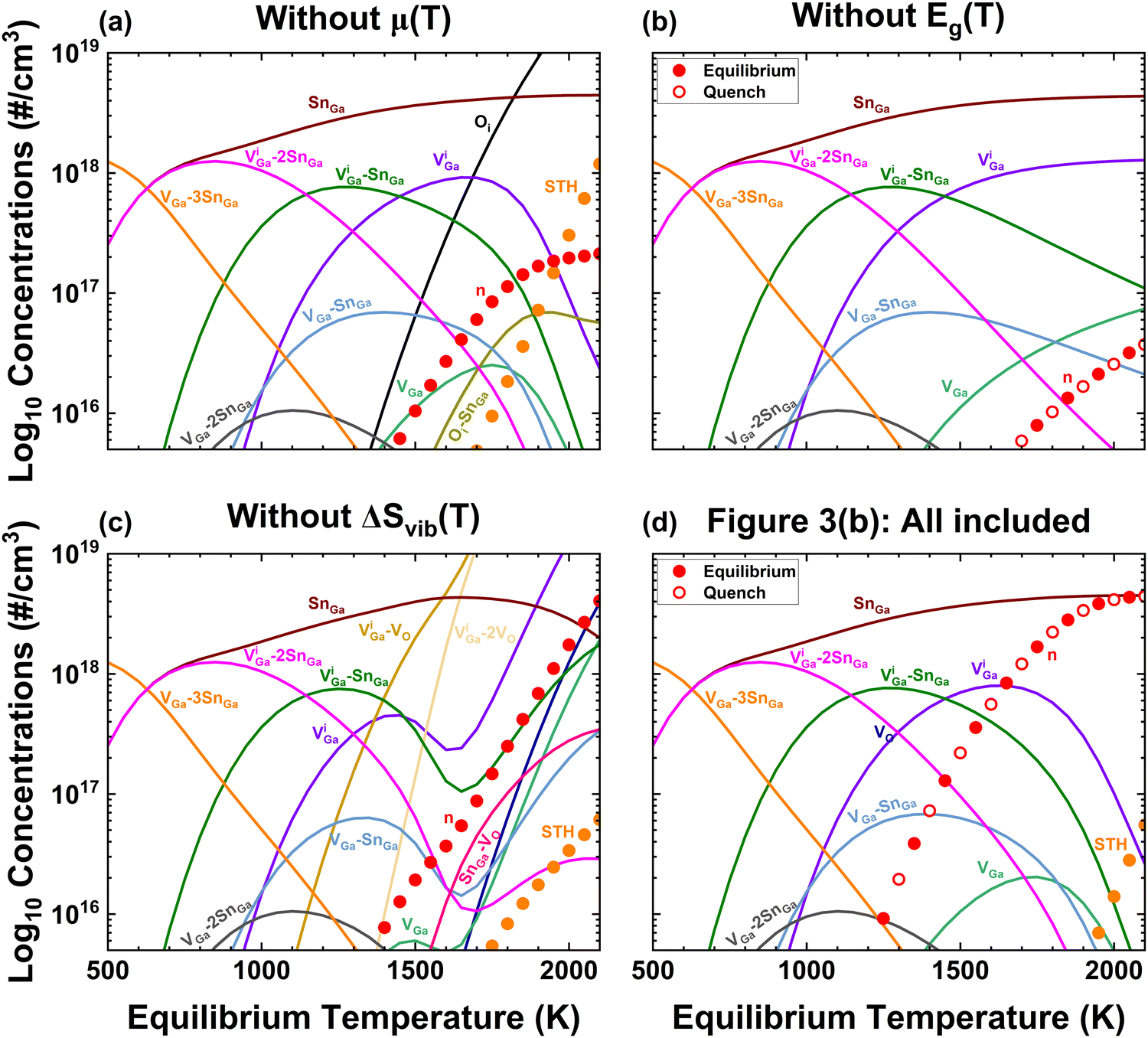 | ||
| Fig. 5 Effects of omitting one temperature dependence at a time to investigate their importances. Conditions kept constant are [Sn] = 4.5 × 1018 cm−3 and f = 0.40. (a) Adopting T-independent O-rich conditions as in Fig. 1(b) predicts Oi are the dominant compensating acceptors at high temperature and at no temperature does n = [Sn]. (b) Effect of Eg(T), NC(T), and NV(T) held constant at 300 K values, again there is no temperature where n = [Sn]. (c) Effect of omitting ΔSvib(T) – here there is only one temperature at which n = [Sn] so coincidence would be required for agreement with experiments. Also, the concentrations of VGa and divacancy complexes increase to at% concentrations, which would be possible to measure. (d) Replication of Fig. 3(b) including all effects to facilitate side-by-side comparison. | ||
Summarizing, we find that agreement of defect modelling for β-Ga2O3 with real-world observations requires including at least (1) kinetic trapping of dopants like Sn rather than assuming equilibrium with competing phases, (2) temperature dependent chemical potentials taken from thermochemistry, and (3) temperature dependent band edges. The other effects discussed help to tune the details of the results herein, but may be more important for other materials and growth situations.
Importance of “real-world” chemical potentials
We now proceed to analyze and discuss the contributions of these temperature-dependent factors and related assumptions about the thermodynamic environment on predicted defect concentrations. Fig. 2(a) shows the differences in chemical potentials vs temperature for oxygen and gallium under different thermodynamic assumptions. The black solid (dashed) lines show ΔμO (ΔμGa) for β-Ga2O3 in equilibrium with “O-rich” conditions discussed in the papers reporting our set of defect formation energies;4–6,8–10 this corresponds to holding the chemical potentials and formation energy of Ga2O3 ( ) constant vs. temperature. Of course, in experiments it is much more common to hold the oxygen partial pressure constant since O2 is a gas. This results in a roughly linearly-decreasing dependence on T which can be estimated as −1 eV per 700 K. The solid red (solid blue) curves show the experimental temperature dependencies for holding pO2 = 0.02 atm constant as in EFG growth and pO2 = 1 atm as during annealing experiments in a tube furnace.42,43 The ΔμGa required to maintain Ga2O3 in equilibrium (neither growing nor decomposing) is shown as dashed red or blue lines, taking into account also the temperature dependence of
  , which is driven by its specific heat capacity (Cp).
The dash-dot green series of Fig. 2(a) shows the temperature dependence of the maximum ΔμSn allowable without precipitation of SnO2 for pO2 = 0.02 atm calculated analogously to ΔμGa. Assuming the concentration of Sn is held constant at [Sn] = 4.5 × 1018 cm−3 for pO2 = 0.02 atm as for Fig. 1(a) produces the non-monotonic solid green curve. This dependence arises from self-consistently solving for both ΔμSn and εF at each temperature thus is a function of both phase thermochemistry and the set of defects and complexes included in the calculation. The crossing point of the green solid and dash-dot curves near 1850 K represents the temperature at which the Sn solubility limit falls below 4.5 × 1018 cm−3, as can be seen in Fig. 1(c). In EFG crystal growth of Sn-doped substrates, the concentration of Sn added to the melt is less than the solubility limit in the solid at Tm, thus at high temperatures [Sn] in the solid is limited by supply in the melt but as the crystal cools the Sn is kinetically trapped at concentrations exceeding the solubility limit simply because the diffusion kinetics become too slow to precipitate 2nd phases.
Fig. 2(b) translates Fig. 2(a) into chemical potential space by parametrically plotting ΔμGa and ΔμO at each temperature. O-rich and Ga-rich conditions are single points, shown for the DFT-calculated ΔHF = −10.22 eV FU−1.5 The diagonal line connecting these two points gives all combinations of ΔμGa and ΔμO satisfying 2ΔμGa + 3ΔμO = ΔHF and moving between the endpoints would correspond to traversing the single-phase β-Ga2O3 field on the T-x phase diagram while remaining in equilibrium. Analogous lines based instead on experimental thermochemistry are presented for 300 and 2100 K; it can be seen that the standard DFT result is a minor underestimate at 300 K but that the discrepancy approaches 50% at high temperatures because of the neglect of phonon specific heat capacity. We note that crystal growth requires at least a slight departure up and right from the equilibrium lines in order to provide a driving force; analogously, decomposition/etching occurs for conditions slightly down and left. The blue (red) data series parametrically plot the temperature dependence of Ga and O chemical potentials for β-Ga2O3 in equilibrium with pO2 = 1 atm (0.02 atm), in correspondence with Fig. 2(a). These do not fall on one diagonal line since  becomes increasingly negative (by >4 eV FU−1) from 300–2100 K. While the locus (ΔμGa, ΔμO) for 1 atm pure O2 is <15% away from “O-rich conditions” at 0 or 300 K, at elevated temperatures constant pO2 experiments have loci many eV away from either O-rich or Ga-rich conditions, translating to enormous differences in predicted defect concentrations (factors >107!). Achieving the “O-rich” conditions presented in DFT papers during bulk crystal growth from the melt would require (1) enormously elevated pO2, (2) use of alternate O sources such as ozone,44,45 or (3) dissociation and or excitation of O2 molecules as in plasma-assisted molecular beam epitaxy (PAMBE). Summarizing, real-world bulk crystal growth or processing conditions are probably quite far from “O-rich” or “Ga-rich” conditions presented in many DFT computation papers, thus large differences in concentrations of defects predicted are to be expected when one or more components of the crystal is not a condensed phase. Growth methods using excited reactants can have higher chemical potentials, but their chemical potential values are difficult to quantify.
Fig. 3 investigates the effect of assumptions about O chemical potential while holding [Sn] = 4.5 × 1018 cm−3 for (a) O-rich conditions, (b) pO2 = 0.02 atm, ptot = 1 atm and (b) pO2 = ptot = 1 atm. To clarify the effects, all native defects were included in calculations but Sn is the only impurity included. The solid red circles show the free electron density n at the given temperature, while open circles represent predicted results for instantaneous quenching from each temperature to 300 K. It is immediately clear from Fig. 3(a) that the assumption of O-rich conditions at crystal growth and cooling temperatures would yield a prediction that Sn-doped crystals should be insulating rather than the commonly-experienced nearly degenerate doping with nearly unmeasurable compensation. Using experimental thermochemical data for pO2 = 0.02 or 1 atm as shown in (b) and (c) results in predictions for both equilibrium and quenching compatible with that real-world observation as long as the defect system freezes-in (for large crystals) somewhere between Tm and ∼1950 K. Please note that the transition temperature at which the ratio n/[SnGa] begins to deviate below 1 changes with the assumption of how much of the temperature dependent bandgap occurs in the conduction band, as discussed in detail in the following section. Fig. 3 assumes 40% (f = 0.40), but plots for f between 0 and 1 are shown in the ESI.† As noted before, we suspect that the native defect system probably freezes-in at the lower end of this range given that DLOS finds VGa-related defects in the low 1016 cm−3 range32 and annealing above ∼900 °C is required to observe changes in conductivity of doped samples and diffusion of substitutional impurities.42,43,46–48 We have performed (unpublished) experiments annealing Sn-doped wafers in 1 atm O2 at 1000–1100 °C. Samples become transparent to the eye and the free carrier absorption becomes undetectable using Fourier transform infrared (FTIR) after 2 weeks. Comparing Fig. 3(b) and (c), this effect is predicted fairly well since the predicted n(T) for both equilibrium and quenching cases is lower at all temperatures for pO2 = 1 atm compared to the 0.02 atm used for EFG growth and reaches the 1016 cm−3 range 1300–1400 K. However, our FTIR experiments indicate that the true carrier density is probably lower, thus some further improvements in our modeling such as details of ΔSvib, fraction f of Eg(T) in the conduction band, hydrogen incorporation, and freeze-out of different defects at different temperatures should be investigated more fully in the future.
Importance of temperature-dependent bandstructure
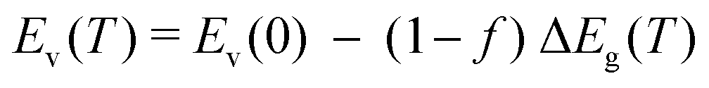
Having examined the effects of different thermodynamic and kinetic constraints on the elements incorporated into the modeling, we now turn attention to the effects of temperature dependence of the bandgap, which in β-Ga2O3 decreases by nearly 2 eV from 300 K to Tm without even accounting for STHs.37 Typical experiments like optical absorption cannot resolve the absolute band edge positions independently; only their difference Eg(T) is accessible. Analogously, DFT using pseudopotentials that exclude deep core levels can result in ambiguity in that different correction schemes for electric potential self-interactions within the supercell may result in conflicting predictions.37 We thus have investigated a range of scenarios in which the temperature dependent change in bandgap ΔEg(T) ≡ Ec(T) − Ev(T) is apportioned such that fraction f occurs in the conduction band and fraction (1−f) occurs in the valence band. With the definitions Ev(0) ≡ 0 and Ec(0) ≡ Eg(0), the absolute positions of the band edges Ec(T) and Ev(T) are given as: | (1a) |
 | (1b) |
 | (1c) |
Fig. 4 shows the dramatic effect exerted by the conduction band's temperature dependence on VGa and its complexes, which are the dominant native defects that compensate shallow n-type dopants. In (a) and (b), we show computed defect concentrations representing EFG growth of crystals doped with [Sn] = 4.5 × 1018 cm−3, assuming ΔEg(T) occurs entirely in the valence band (f = 0) in (a) and entirely in the conduction band (f = 1) in (b). The conditions are the same as in Fig. 1(a). Since εF is in the top half of the bandgap for n-type doping, changes in EV with temperature have no effect on the net doping ND–NA and charge balance demands large concentrations of compensating VGa and complexes with Sn. However, changes in EC with temperature dramatically suppress these native defects. This is one of the strongest effects we infer must be occurring in real crystals; without it, Sn-doped wafers grown by EFG should be heavily compensated as in (a) and DLOS experiments should reveal EC-2 eV trap numbers approaching 1018 cm−3. Large values of f suppress VGa compensating defects sufficiently for the appearance of a wide temperature range over which the defect system can freeze-in and result in n = [Sn] at room temperature (ESI†). Larger values of f (>0.50) predict less sensitivity to the freezing-in temperature of compensating defects for Sn-doped EFG crystals and thus the as-grown behavior. However, smaller values of f are required to simultaneously give agreement that 1300–1400 °C O2 annealed samples should be insulating – thus the annealing experiments provide more stringent constraints on the overall model. The ESI† shows cases for pO2 = 1 atm for f values of 0, 0.5 and 1. We determined our most-likely estimate for f = 0.40 (±0.05 or so) as the value that best satisfies the two experimental constraints simultaneously (given all the other model assumptions). Lee et al.37 concluded from DFT calculations that most of the temperature dependence of the bandgap occurs in the valence band, although an alternate absolute potential alignment scheme discussed in that work predicted the opposite. Fig. 4(a) shows that setting f = 0 is inconsistent with conducting EFG Sn-doped samples, which is one of the main experimental observations. Thus, our modelling provides circumstantial evidence for the valence band contributing slightly more than half, but direct experimental investigations using e.g. X-ray techniques would be desirable. Our mode-counting of simple quantum oscillators treatment of ΔSvib suppresses complexes including VO at high temperature, which will affect the predicted compensation if crystals were quenched rapidly. Fig. 5 delves further into the range of models yielding agreement with experimental observations.
Fig. 4(c) shows the temperature dependent band diagram including Fermi energy corresponding to parts (a) and (b) and, with (d), explains the mechanism behind VGa suppression. The black thin (thick) lines show EC and EV for f = 0 (f = 1), while red lines show the solution for εF in both cases. For f = 1, the fact that we impose [Sn] = constant becomes important, since EC − εF = kBT![[thin space (1/6-em)]](https://www.rsc.org/images/entities/i_char_2009.gif) ln(n/NC(T)), in the absence of strong compensation εF will follow the temperature dependence of EC. Examining part (d) makes the mechanism apparent; as EC and εF shift down at high temperatures (by nearly 2 eV from 0 K for f = 1), the formation energies of the dominant VGa,ic3−, (VGa,ic–SnGa)2−, and (VGa,ic–2SnGaII)1− increase by approximately 6, 4, and 2 eV respectively, resulting in their near-total suppression and prevention of native defect compensation at high temperatures. The case of growth of β-Ga2O3 from the melt provides an extreme case of the importance of including temperature dependent band edges in defect modelling because of its high Tm and strong electron–phonon coupling,3,37 but we recommend that this effect should be more routinely included in defect concentration modelling. If ΔSvib and E° (see eqn (2) in Computational methods) differ for different charge states, the charge transition level between them will become temperature-dependent.49 KROGER has the capability to incorporate such temperature-dependent formation energies, which represent one of the next frontiers in defect energy calculations.
ln(n/NC(T)), in the absence of strong compensation εF will follow the temperature dependence of EC. Examining part (d) makes the mechanism apparent; as EC and εF shift down at high temperatures (by nearly 2 eV from 0 K for f = 1), the formation energies of the dominant VGa,ic3−, (VGa,ic–SnGa)2−, and (VGa,ic–2SnGaII)1− increase by approximately 6, 4, and 2 eV respectively, resulting in their near-total suppression and prevention of native defect compensation at high temperatures. The case of growth of β-Ga2O3 from the melt provides an extreme case of the importance of including temperature dependent band edges in defect modelling because of its high Tm and strong electron–phonon coupling,3,37 but we recommend that this effect should be more routinely included in defect concentration modelling. If ΔSvib and E° (see eqn (2) in Computational methods) differ for different charge states, the charge transition level between them will become temperature-dependent.49 KROGER has the capability to incorporate such temperature-dependent formation energies, which represent one of the next frontiers in defect energy calculations.
Relative importances of temperature dependent factors
Fig. 5 investigates the criticality of including various temperature-dependent parameters – Δµ(T), Eg(T), and ΔSvib(T) – in achieving agreement with experimental observations. In each subfigure unless noted, [Sn] = 4.5 × 1018 cm−3, pO2 = 0.02 atm as for EFG, and f = 0.40 are used. Fig. 3(b) provides the results when all three temperature-dependent effects are included, and is replicated as Fig. 5(d) to facilitate side-by-side comparison. Fig. 5(a) includes Eg(T) with f = 0.40 (and the T3/2 dependencies of Nc and Nv) and the quantum estimate for ΔSvib but keeps chemical potentials constant at the DFT-estimated 0 K values (ΔμGa = −5.11 eV and ΔμO = 0 for O-rich conditions). Despite the fact that the VGa are suppressed at high temperatures, agreement with reality could not be found as n ≪ [Si] for all temperatures. Notably also, the unrealistically-high ΔμO compared even to pure oxygen conditions (see Fig. 2) causes Oi to provide compensation at high temperatures rather than VGa related defects including VGa–VO divacancies.4 Oi is believed to have extremely low migration energies,50 thus is expected remain equilibrated even at room temperature, however if other compensators like VGa are suppressed at high temperature because of the presence of Oi but frozen in, the presence of Oi can still change the defects present at 300 K. Thus, it would not be proper to build reduced models in which Oi was omitted. This is one example why we favor avoiding a-priori assumptions regarding dominant defects. KROGER is sufficiently computationally efficient that dominant defects and reduced models may be identified after the fact without significant delays.Fig. 5(b) includes temperature dependent chemical potentials for O-rich conditions (p = 0.02 atm pure O2 as in Fig. 2), but assumes a temperature-independent bandgap and density of states values. There is no possibility of agreement with real-world Sn-doped wafers since n ≪ [Sn] for all temperatures for equilibrium or full quenching. Finally in Fig. 5(c), temperature dependent band parameters and realistic chemical potentials are incorporated but ΔSvib is omitted. Here agreement with experiment is possible, but only if the defect system happens to coincidentally freeze in at one specific temperature. Notably, concentrations of VGa and divacancy complexes increase to at% concentrations which we believe would have been observed if actually present in real-world samples.
Thus, at least for the case of heavily Sn-doped EFG grown crystals, the real-world temperature dependencies of chemical potentials and bandstructure are absolute requirements for quantitative defect modelling. The role of ΔSvib is also clearly very important, but we hesitate to draw absolute conclusions because of the oversimplicity of our treatment herein; we eagerly await developments in efficient but high-fidelity computation of defect vibrational spectra. Versions of Fig. 5(a) and (c) for a range of f from 0 to 1 are presented in the ESI.†
Modeling unintentionally-doped (UID), Fe-doped, and Mg-doped crystals
Fig. 6 investigates defects predicted for cases of unintentionally-doped (UID), Fe-doped and Mg-doped β-Ga2O3 grown by EFG, with non-dopant-related model parameters fixed at the values determined in Fig. 1(a) unless otherwise noted. The results agree with real-world observations that UID are conducting while Fe and Mg-doped β-Ga2O3 are insulating. In Fig. 6(a), the UID case is assumed to have dominant impurities [Si] = 2.3 × 1017 cm−3, [Mg] = 5 × 1015 cm−3 and [Fe] = 3 × 1016 cm−3,33 and a wide range of temperatures yield equilibrium n = [Si] down to 1700 K. Note that equilibrium n and STH concentrations exceed the low, unintentional [Si] at the highest temperatures; since both electrons and STHs can equilibrate from any processing temperature this is of no consequence at room temperature. In (b), [Fe] = 2.5 × 1018 cm−3 and [Si] = 2.3 × 1017 cm−3 for all temperatures while in (c) [Mg] = 2 × 1018 cm−3 and [Si] = 2.3 × 1017 cm−3.1,51 Due to the lack of detailed data on other unintentional impurities in such crystals, (b) and (c) can be considered as hypothetical, assuming that the inclusion of Ir and other impurities remain constant. For Fe-doped (b) and Mg-doped (c), electron concentrations fall to immeasurable values by 300 K for both cases whether cooled slowly or quenched, thus both would be insulating for any cooling rates. The main difference compared to the nearly-degenerately Sn-doped cases above is the greater role played by STHs because their numbers either exceed the doping in the case of UID, or because of the acceptor dopants in the Fe and Mg cases. Thus, our modelling reproduces the major known aspects of defect quantities in Sn-, Fe-, Mg- and UID EFG-grown crystals. In the ESI,† we additionally model Bridgeman growth in Pt/Rh crucibles at pO2 = 1 atm. Follow-on modelling of epitaxially-grown crystals by various methods would help to provide additional constraints on our quantitative defect modelling.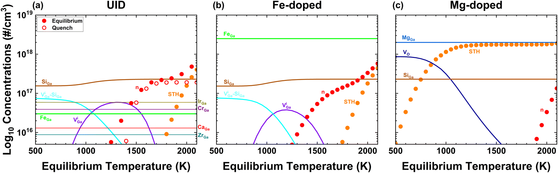 | ||
| Fig. 6 Calculated defect concentrations for EFG grown (pO2 = 0.02 atm) (a) UID, (b) Fe-doped Ga2O3 and (c) Mg-doped Ga2O3. Background impurities have concentrations as in Fig. 1(a), while [Fe] and [Mg] were set to 3 × 1016 cm−3 and 5 × 1015 cm−3. The predicted carrier densities are in good agreement; n = [Si] for UID while immeasurable carrier densities should be present for Fe and Mg doped which is consistent with them being insulating. | ||
Conclusions
We quantitatively modeled point defect concentrations in β-Ga2O3 by combining formation energies from DFT using hybrid functionals with advanced thermodynamic modelling using a new program we dub KROGER. We find that, to achieve agreement with real-world experience that Sn-doped wafers are conductive with n = [Sn], many oft-neglected temperature-dependent effects must be included and that constant concentration rather than constant-chemical potential thermodynamic conditions are more appropriate for describing [Sn]. Extensive thermochemical data is available for many semiconductors; using this data to compute temperature- and pressure-dependent chemical potentials allows high-fidelity modelling of specific growth and processing. Including Eg(T) is also critical because it suppresses VGa that would otherwise strongly compensate the n-type doping. We included a simple, minimal estimate of defect ΔSvib based on counting quantum oscillator modes per atom which is especially important for divacancies and other large complexes. Especially for oxides like β-Ga2O3 for which crystal growth occurs at very high temperatures, TΔSvib amounts to 1–2 eV thus while computationally-demanding calculations are required, accurately computing this factor will be critical to advancing defect modelling. We have demonstrated a framework and workflow for high-fidelity modelling of defect concentrations in semiconductors, which we anticipate will be extremely useful in moving defect computations from qualitative insights to quantitative process-dependent predictions.Calculation methods
Formation free energy of defects
The formation energy of isolated, dilute defects in crystals can be computed under either isobaric (Gibbs energy) or isochoric (Helmholtz energy) constraints. The total free energy of the qth charge state of the jth defect or complex is given as: | (2) |
 is the finite-size corrected formation energy in the dilute limit for a Fermi level (εF) evaluated at the position of the valence band maximum (εv)52 herein calculated using DFT with Heyd–Scuzeria–Ernzerhof (HSE)53,54 hybrid functionals, ΔεF represents the Fermi energy (chemical potential for electrons) relative to the electrochemical energy reference (εF − εv) used for
  , Δμi is the chemical potential of element i referenced to its standard state, mi,j is the number of i atoms added (+) or removed (−) to form the jth defect or complex, and ΔSvibj,q is the associated change in vibrational entropy of the crystal. ΔSvibj,q may be sensitive to isochoric versus isobaric conditions for anharmonic bonding and remains computationally demanding to compute accurately for isolated defects at useful levels of theory (e.g. using HSE and very large supercells).
The defect formation energies used in this work were taken from a consistent set of hybrid functional (HSE06) calculations reported previously.4–6,8–10 These studies follow established practices for first-principles defect modeling, including the use of large supercells, appropriate k-point sampling, full atomic relaxation, and charge correction schemes such as the Freysoldt–Neugebauer–Van de Walle method. While specific computational parameters may vary slightly among different defect types, the dataset provides a uniform and reliable foundation for the thermodynamic modeling presented here.
Defect concentrations
In the dilute limit, the number of each charge state q of defect j (nj,q) is given by: | (3) |
We use the number density of appropriately-sized unit cells Nj,q as the basis for each defect or complex since some large complexes may require multiple primitive cells (or equivalently, lattice sites or formula units). For example, we consider complexes containing up to 3SnGa donors bound to a VGa, which would require between 2 and 4 formula units depending on whether each of these 4 elementary defects entities occupy Ga1 or Ga2 sites. In other words, the numerical prefactor commonly taken as Nsites should vary for large complexes. Additional degeneracy factors for configurational, electronic, and spin degrees of freedom are combined into θj,q.55 All calculations in this paper included a set of 873 charge states comprising 259 defects and complexes and 19 elements in β-Ga2O3. Most (but not all) have been previously published in Varley et al.,8–10 and Frodason et al.,4–6 the formation energies are provided for all of these defects in the ESI.† The formation energy of β-Ga2O3 was calculated for the same supercells as −10.22 eV per formula unit (FU), which is close to but lower than the experimentally measured value at 300 K.
We also implemented self trapped holes (STH) as new categories of electronic defects in addition to the usual free electrons and holes whose numbers are calculated from effective conduction band and valence band densities of states, respectively. The self-trapping energies for STH on OI and OII sites are taken as 0.53 & 0.52 eV.30,31 An important detail is that, in thermal equilibrium, both band holes and self-trapped holes are equally-accessible microstates for electron–hole pair excitation of the perfect crystal. Since every OI and OII atom is capable of localizing a STH and in the fully-localized limit they will form a dispersionless band, the prefactor for each STH type is the primitive unit cell density 1.91 × 1022 cm−3 rather than the effective valence band density of states =1.71 × 1020 cm−3 we adopt herein for band holes.56 While optical excitations measure the “bandgap” of β-Ga2O3 to be 4.8–5 eV (strongly modified by Urbach tails3), from the standpoint of calculating the intrinsic carrier density the “bandgap” is arguably 0.53 eV lower because thermal excitations can create STH's while photons cannot. Because the intrinsic carrier density including STH (ni,STH) approaches ∼1017 cm−3 near Tmelt, this slightly affects defect equilibrium at high temperatures but does not change any major findings herein although it may for cases of lower impurity doping concentrations.
Charge neutrality and quenched concentrations
Within the usual grand-canonical formalism, the simplest defect equilibrium problem is full equilibrium at a given temperature with chemical potentials specified for all elements. Each charge state included in modeling adds one unknown concentration but also one equation of the form eqn (3). However, Ej,q for nonzero charge states depends on the additional unknown εF, thus the final equation allowing implicit solution of the system of equations comes from charge balance, e.g. solving the charge-neutrality condition: | (4) |
Eqn (3) can be overridden with fixed values if the concentrations of some charge states should be held constant. If the total concentration nj,tot of a defect j composed of multiple charge states (given by  ) should be held constant, this is accomplished by overriding eqn (3) with values from the Gibbs distribution:
 | (5) |
This allows modelling temperature dependent defect concentrations in cases where certain defects stop equilibrating below some temperature but the charge in defect j still changes with temperature. Full quenching a system of defects from a processing temperature to a final temperature (usually 300 K) is accomplished by using eqn (5) for all defects in the model with the nj,tot determined at the high temperature. The total concentration of impurity i contained in all defects in the model is of course simply the number of i atoms per defect j times the total defect j concentration, summed over all defects in the model:
 | (6) |
For the host material elements, this sum must be added to the numbers of atoms in non-defective unit cells.
Specification of chemical potentials or concentrations for elements
In a grand canonical formulation of point defect formation, it is assumed that atoms are exchanged between the crystal and reservoirs setting chemical potentials for each element until equilibrium is reached. It is common (but not universal) in DFT-based work on defects to compute temperature-independent formation energies of all phases also using DFT and then evaluate temperature dependent defect concentrations in rich/poor chemical potential limits for each element. Using temperature-independent chemical potentials assumes that the specific heats of all relevant compounds are negligible. For gaseous reactants, this is corrected for the ideal gas translational kinetic energy contribution , but for multiatomic molecules and high temperatures, the contributions of rotovibrational and electronic excitations also contribute. These can be challenging to compute accurately, so we adopted a pragmatic approach recognizing that for many materials of interest, experimental temperature- and pressure-dependent thermochemical data such as standard Gibbs energies (G°(T,P)) are available that have been validated to reproduce the materials’ phase diagrams. Zinkevich and Adlinger assessed the thermodynamics of the Ga–O binary system (referenced to 0 K) and we adopt their temperature-dependent parameterizations.35 Values for competing phases involving impurities were taken from the Fact Sage database.57 The fact that oxygen is a gas for all growth conditions means that temperature and partial pressure significantly change its chemical potential
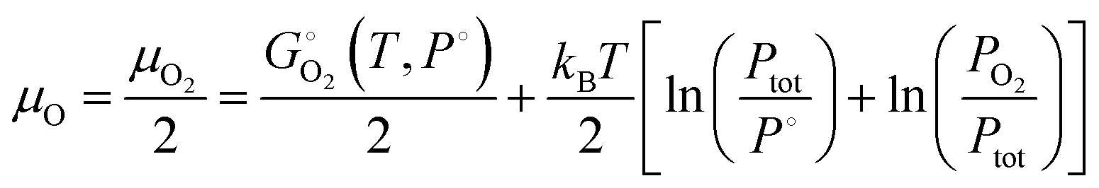 | (6a) |
 | (6b) |
 is the standard Gibbs energy as function of temperature, P° is the reference pressure (e.g. 1 atm), pO2 is the oxygen partial pressure, and in eqn (6a) we have avoided cancelling out Ptot to clarify the roles of total and partial pressures (which can become confusing especially when equilibrium vapors such as Ga2O + O2 resulting from Ga2O3 decomposition are considered35,36,58). The temperature dependencies from rotovibrational and electronic degrees of freedom are contained in
  . If the reference temperature for the thermochemical data is not 0 K then the defect formation energy from the elements should be corrected by
  . For ternary and more complex materials and for novel materials, this data may not exist thus computation of the formation free energy is required.59
Each growth or annealing process we considered occurs under well-defined temperature, total pressure, and oxygen partial pressure (pO2), allowing us to determine the excess chemical potential for oxygen ΔμO in eqn (6b) in equilibrium with β-Ga2O3. Calculations may be made for values of chemical potentials anywhere within the boundaries of the β-Ga2O3 single phase field. At high temperatures, β-Ga2O3 may be in equilibrium with Ga(vap), GaO(vap) or Ga2O(vap) on the Ga-rich side and with O2(g) on the O-rich side, depending on the experiment. For all growth processes herein, pO2 is controlled directly so ΔμGa is determined from the formation reaction
 | (7a) |
 | (7b) |
Only for pO2 lower than all cases herein does decomposition into Ga2O and O2
| Ga2O + O2 ⇌ Ga2O3 | (7c) |
Vibrational entropy
In lieu of directly computing the vibrational energy changes associated with each chargestate, we adopt a simple quantum oscillator model62 to calculate the vibrational entropy (ΔSvibj,q) using one representative phonon frequency ω0 for the solid rather than the detailed phonon band structure.55 Each atom in the perfect lattice adds 3 degenerate modes at ω0; therefore forming a vacancy subtracts 3, an interstitial adds 3, a substitutional defect does not change the number of modes, and complexes add or subtract modes according to the net change in number of atoms. Because of our lack of information regarding bond stiffness changes, herein we only count changes in numbers of “average” modes rather than taking into account mode frequency changes. Such information can readily be incorporated, as can integration over phonon bandstructures for perfect and defective supercells.Within our simple treatment, the vibrational entropy and isochoric specific heat per atom are:
 | (8) |
 | (9) |
Mass and bonding changes will indubitably result in different magnitudes and even different signs of ΔSvib64,65 for different charge states. Improved calculations of ΔSvib using hybrid functionals or higher levels of theory for dominant defects and complexes is one of the final frontiers for refinement of the modelling herein. We note that crystal growth experiments are nearly always done at controlled by pressure rather than volume; thus computations should reflct consistent assumptions. The difference between the two is related to thermal expansion and constant pressure conditions would in general tend to lower phonon frequencies since interatomic energy vs. distance curves soften at larger distances. Thus our treatment can also be improved by computing ΔSvib for different lattice constants taking into account (anisotropic) thermal expansion.
Temperature dependence of bandgap
Both bandgap and effective densities of states are strong functions of temperature; many semiconductors exhibit a change in bandgap ΔEg(T) on the order of −0.1 eV per 300 K, which can be parameterized using e.g. the Varshini or Einstein–Debye equations37,66 (we used the Varshini values from Lee et al.37). We establish a shared absolute energy scale with 0 fixed at Ev(0) such that both band edges and chargestate formation energies and associated charge transition levels may all have individual temperature dependencies. Because the individual contributions of the valence and conduction bands are not definitively known for β-Ga2O3, we introduce the unknown parameter f as the fraction of ΔEg(T) arising from the conduction band, as shown in eqn (1).1,37,67This allows the individual band edges, which determine the effective formation energies68 of band holes and electrons, to change with temperature on the same energy scale as the formation energies (and thus densities) of defect chargestates. The extremal cases for f = 0 and f = 1 are depicted in Fig. 4(c). The effective density of states for isotropic, parabolic bands has T3/2 dependence; users may define other more detailed functions additionally, for example including band non-parabolicity or even direct integration of a computed density of states times occupation function. For generality we utilize Fermi–Dirac statistics for band carriers and also can include degenerate statistics for site occupation by defects69 if required. Based on computed effective masess for band electrons and holes, we adopted values of NC = 3.33 × 1018 cm−3 and NV = 1.71 × 1020 cm−3![[thin space (1/6-em)]](https://www.rsc.org/images/entities/char_2009.gif) 56 at 300 K and the bandgap at 0 K as Eg = 5.1 eV70
56 at 300 K and the bandgap at 0 K as Eg = 5.1 eV70
Solution methods
For full equilibrium calculations in which all elements are specified by chemical potentials, only eqn (4) must be solved; KROGER's default method is Matlab's fzero function. An initial εF guess is generated by computing the net charge on a grid spanning from Ev to Ec, plus 5 kBT on either side and taking the point where the sign changes. The direct search is done because commonly the net charge barely changes with εF over much of the bandgap so traditional downhill optimization methods may stall out unless good initial guesses close to the solution are given. Calculating defect equilibrium with some element concentrations specified is more challenging as it requires simultaneously solving for the εF and corresponding chemical potentials (e.g. ΔμSn herein) that satisfy charge balance and yield the specified total element concentration across all defects. In KROGER this is achieved by minimizing a composite objective function composed of the absolute value of net charge (right side of eqn (4)) plus the absolute value(s) of the deviation(s) of concentration(s) of the fixed element(s) from their target number(s) (for each element, eqn (6) minus the target value). Because of the exponential dependence of concentrations on εF and chemical potentials, the solution is typically located in extremely narrow hypervalleys of width <kBT surrounded by large hyperareas having ∼0 gradient; thus self-consistent solution requires rather exhaustive searches of the parameter space. KROGER retains a brute-force grid search option but we have found that particle swarm optimization followed by a traditional simplex optimization balances accurate convergence with speed. Calculations versus temperature are done efficienctly by exploiting continuity by proceeding from high to low temperature using the prior solution as the guess for εF and Δμ. Solutions are accepted when the composite objective function is of order 103–106 cm−3, which is at least 6–8 orders of magnitude less than practically-measurable concentrations.Uncertainty estimates
Despite thorough optimization with the model described above, some uncertainties in parameter values remain. Based on sensitivity analysis and the magnitude of free energy terms, we estimate the uncertainties in TΔSvib at Tm for each charge state to be ±1 eV because of our crude approximate model, the uncertainty in the thermal bandgap energy Eg to be ±0.3 eV (including the issues of STHs mentioned) and the uncertainties related to the HSE-calculated charge state formation energies to be ±0.5 eV.49 We have carefully assessed that the impact, even when these are compounded, on the major findings herein is minimal. For example electron density n at 1300–2100 K changes by only a small factor 0.5–2× for Sn-doped samples because of the constraint of charge balance. Addressing these uncertainties represents frontiers of defect computation and will lead to even more accurate predictions.Data availability
The defect properties including HSE-computed formation energies are available in the ESI.† The KROGER code is available at https://github.com/mikescarpulla/KROGER.Conflicts of interest
There are no conflicts to declare.Acknowledgements
This work was supported by funding from the Air Force Office of Scientific Research under MURI award no. FA9550-21-0078 (Program Manager: Dr Ali Sayir). The work of J. B. V. was performed under the auspices of the US DOE by Lawrence Livermore National Laboratory under contract DE-AC52-07NA27344 and partially supported by LLNL LDRD Funding under Project 22-SI-003 and by the Critical Materials Institute, an Energy Innovation Hub funded by the U.S. DOE, Office of Energy Efficiency and Renewable Energy, Advanced Materials and Manufacturing Technologies Office. Financial support is acknowledged from the Research Council of Norway through the GO-POW project (grant no. 314017). Computations were performed on resources provided by UNINETT Sigma2 – the National Infrastructure for High Performance Computing and Data Storage in Norway.References
- T. Onuma, S. Fujioka, T. Yamaguchi, M. Higashiwaki, K. Sasaki, T. Masui and T. Honda, Correlation between Blue Luminescence Intensity and Resistivity in β-Ga2O3 Single Crystals, Appl. Phys. Lett., 2013, 103(4), 041910, DOI:10.1063/1.4816759.
- N. Ueda, H. Hosono, R. Waseda and H. Kawazoe, Synthesis and Control of Conductivity of Ultraviolet Transmitting β-Ga2O3 Single Crystals, Appl. Phys. Lett., 1997, 70(26), 3561–3563, DOI:10.1063/1.119233.
- A. Islam, N. D. Rock and M. A. Scarpulla, Quantification of the Strong, Phonon-Induced Urbach Tails in β-Ga2O3 and Their Implications on Electrical Breakdown, J. Appl. Phys., 2024, 136(3), 035701, DOI:10.1063/5.0211588.
- Y. K. Frodason, C. Zimmermann, E. F. Verhoeven, P. M. Weiser, L. Vines and J. B. Varley, Multistability of Isolated and Hydrogenated Ga–O Divacancies in β-Ga2O3, Phys. Rev. Mater, 2021, 5(2), 025402, DOI:10.1103/PhysRevMaterials.5.025402.
- Y. K. Frodason, P. P. Krzyzaniak, L. Vines, J. B. Varley, C. G. Van De Walle and K. M. H. Johansen, Diffusion of Sn Donors in β-Ga2O3, APL Mater., 2023, 11(4), 041121, DOI:10.1063/5.0142671.
- Y. K. Frodason, J. B. Varley, K. M. H. Johansen, L. Vines and C. G. Van De Walle, Migration of Ga Vacancies and Interstitials in β-Ga2O3, Phys. Rev. B, 2023, 107(2), 024109, DOI:10.1103/PhysRevB.107.024109.
- H. Peelaers, J. L. Lyons, J. B. Varley and C. G. Van De Walle, Deep Acceptors and Their Diffusion in Ga2O3, APL Mater., 2019, 7(2), 022519, DOI:10.1063/1.5063807.
- J. B. Varley, First-Principles Calculations 2, in Gallium Oxide: Materials Properties, Crystal Growth, and Devices, ed. M. Higashiwaki and S. Fujita, Springer International Publishing, Cham, 2020, vol. 293, pp. 329–348 DOI:10.1007/978-3-030-37153-1_18.
- J. B. Varley, H. Peelaers, A. Janotti and C. G. Van De Walle, Hydrogenated Cation Vacancies in Semiconducting Oxides, J. Phys.: Condens. Matter, 2011, 23(33), 334212, DOI:10.1088/0953-8984/23/33/334212.
- J. B. Varley, J. R. Weber, A. Janotti and C. G. Van De Walle, Oxygen Vacancies and Donor Impurities in β-Ga2O3, Appl. Phys. Lett., 2010, 97(14), 142106, DOI:10.1063/1.3499306.
- X. Zhang, J. Kang and S.-H. Wei, Defect Modeling and Control in Structurally and Compositionally Complex Materials, Nat. Comput. Sci., 2023, 3(3), 210–220, DOI:10.1038/s43588-023-00403-8.
- Novel Crystal Technology, Inc. | Creating Gallium oxide will create a new futuristic way of living, https://www.novelcrystal.co.jp/eng/ (accessed 2024-01-25).
- S. Lany, Defect Phase Diagram for Doping of Ga 2 O 3, APL Mater., 2018, 6(4), 046103, DOI:10.1063/1.5019938.
- C. Freysoldt, B. Grabowski, T. Hickel, J. Neugebauer, G. Kresse, A. Janotti and C. G. Van De Walle, First-Principles Calculations for Point Defects in Solids, Rev. Mod. Phys., 2014, 86(1), 253–305, DOI:10.1103/RevModPhys.86.253.
- D. Wickramaratne and J. L. Lyons, Assessing the SCAN Functional for Deep Defects and Small Polarons in Wide Band Gap Semiconductors and Insulators, Phys. Rev. B, 2024, 109(24), 245201, DOI:10.1103/PhysRevB.109.245201.
- V. Stevanović, S. Lany, X. Zhang and A. Zunger, Correcting Density Functional Theory for Accurate Predictions of Compound Enthalpies of Formation: Fitted Elemental-Phase Reference Energies, Phys. Rev. B: Condens. Matter Mater. Phys., 2012, 85(11), 115104, DOI:10.1103/PhysRevB.85.115104.
- Y. Kumagai and F. Oba, Electrostatics-Based Finite-Size Corrections for First-Principles Point Defect Calculations, Phys. Rev. B: Condens. Matter Mater. Phys., 2014, 89(19), 195205, DOI:10.1103/PhysRevB.89.195205.
- GitHub – KROGER: Program for computing full and partial equilibria of point defects in solids, https://github.com/mikescarpulla/KROGER (accessed 2024-09-15).
- P. C. Bowes, G. H. Ryu, J. N. Baker, E. C. Dickey and D. L. Irving, Fermi Level Pinning in Co-Doped BaTiO3: Part II. Defect Chemistry Models, J. Am. Ceram. Soc., 2021, 104(11), 5859–5872, DOI:10.1111/jace.17938.
- F. A. Kröger and N. H. Nachtrieb, The Chemistry of Imperfect Crystals, Phys. Today, 1964, 17(10), 66–69, DOI:10.1063/1.3051186.
- F. A. Kröger, Point Defects in Solids: Physics, Chemistry, and Thermodynamics, Point Defects in Minerals, American Geophysical Union (AGU), 1985, pp. 1–17 DOI:10.1029/GM031p0001.
- S. R. Kavanagh, A. G. Squires, A. Nicolson, I. Mosquera-Lois, A. M. Ganose, B. Zhu, K. Brlec, A. Walsh and D. O. Scanlon, Doped: Python Toolkit for Robust and Repeatable Charged Defect Supercell Calculations, J. Open Source Softw., 2024, 9, 6433, DOI:10.21105/joss.06433.
- J. Buckeridge, Jbuckeridge/Sc-Fermi, 2023, https://github.com/jbuckeridge/sc-fermi (accessed 2024-06-13).
- T. Ogawa, A. Taguchi and A. Kuwabara, An Extended Computational Approach for Point-Defect Equilibria in Semiconductor Materials, npj Comput. Mater., 2022, 8(1), 79, DOI:10.1038/s41524-022-00756-0.
- M. Y. Toriyama, J. Qu, L. C. Gomes and E. Ertekin, VTAnDeM: A Python Toolkit for Simultaneously Visualizing Phase Stability, Defect Energetics, and Carrier Concentrations of Materials, Comput. Phys. Commun., 2023, 287, 108691, DOI:10.1016/j.cpc.2023.108691.
- V. Stevanovic, A Python Code for Calculating the Mean-Value (Baldereschi's) Point for Any Crystal Structure, arXiv May 1, 2024, https://arxiv.org/abs/2405.00925 (accessed 2024-06-13).
- Y. Ma, H. Yu, Y. Zhong, S. Chen, X. Gong and H. Xiang, Transferable Machine Learning Approach for Predicting Electronic Structures of Charged Defects, Appl. Phys. Lett., 2025, 126(4), 044103, DOI:10.1063/5.0242683.
- B. Medasani, Mbkumar/Pycdt, 2024, https://github.com/mbkumar/pycdt (accessed 2024-06-13).
- J. N. Baker, P. C. Bowes, J. S. Harris and D. L. Irving, An Informatics Software Stack for Point Defect-Derived Opto-Electronic Properties: The Asphalt Project, MRS Commun., 2019, 9(3), 839–845, DOI:10.1557/mrc.2019.106.
- J. B. Varley, A. Janotti, C. Franchini and C. G. Van De Walle, Role of Self-Trapping in Luminescence and p -Type Conductivity of Wide-Band-Gap Oxides, Phys. Rev. B: Condens. Matter Mater. Phys., 2012, 85(8), 081109, DOI:10.1103/PhysRevB.85.081109.
- T. Gake, Y. Kumagai and F. Oba, First-Principles Study of Self-Trapped Holes and Acceptor Impurities in Ga2O3 Polymorphs, Phys. Rev. Mater., 2019, 3(4), 044603, DOI:10.1103/PhysRevMaterials.3.044603.
- J. M. Johnson, Z. Chen, J. B. Varley, C. M. Jackson, E. Farzana, Z. Zhang, A. R. Arehart, H.-L. Huang, A. Genc, S. A. Ringel, C. G. Van De Walle, D. A. Muller and J. Hwang, Unusual Formation of Point-Defect Complexes in the Ultrawide-Band-Gap Semiconductor β-Ga2O3, Phys. Rev. X, 2019, 9(4), 041027, DOI:10.1103/PhysRevX.9.041027.
- A. Kuramata, K. Koshi, S. Watanabe, Y. Yamaoka, T. Masui and S. Yamakoshi, High-Quality β-Ga2O3 Single Crystals Grown by Edge-Defined Film-Fed Growth, Jpn. J. Appl. Phys., 2016, 55(12), 1202A2, DOI:10.7567/JJAP.55.1202A2.
- K. Hoshikawa, T. Kobayashi, Y. Matsuki, E. Ohba and T. Kobayashi, 2-Inch Diameter (1 0 0) β-Ga2O3 Crystal Growth by the Vertical Bridgman Technique in a Resistance Heating Furnace in Ambient Air, J. Cryst. Growth, 2020, 545, 125724, DOI:10.1016/j.jcrysgro.2020.125724.
- M. Zinkevich and F. Aldinger, Thermodynamic Assessment of the Gallium–Oxygen System, J. Am. Ceram. Soc., 2004, 87(4), 683–691, DOI:10.1111/j.1551-2916.2004.00683.x.
- R. P. Burns, Systematics of the Evaporation Coefficient Al2O3, Ga2O3, In2O3, J. Chem. Phys., 1966, 44(9), 3307–3319, DOI:10.1063/1.1727229.
- C. Lee, N. D. Rock, A. Islam, M. A. Scarpulla and E. Ertekin, Electron–Phonon Effects and Temperature-Dependence of the Electronic Structure of Monoclinic β-Ga2O3, APL Mater., 2023, 11(1), 011106, DOI:10.1063/5.0131453.
- J. Buckeridge, Equilibrium Point Defect and Charge Carrier Concentrations in a Material Determined through Calculation of the Self-Consistent Fermi Energy, Comput. Phys. Commun., 2019, 244, 329–342, DOI:10.1016/j.cpc.2019.06.017.
- Z. Galazka, K. Irmscher, R. Uecker, R. Bertram, M. Pietsch, A. Kwasniewski, M. Naumann, T. Schulz, R. Schewski, D. Klimm and M. Bickermann, On the Bulk β-Ga2O3 Single Crystals Grown by the Czochralski Method, J. Cryst. Growth, 2014, 404, 184–191, DOI:10.1016/j.jcrysgro.2014.07.021.
- Z. Galazka, K. Irmscher, R. Schewski, I. M. Hanke, M. Pietsch, S. Ganschow, D. Klimm, A. Dittmar, A. Fiedler, T. Schroeder and M. Bickermann, Czochralski-Grown Bulk β-Ga2O3 Single Crystals Doped with Mono-, Di-, Tri-, and Tetravalent Ions, J. Cryst. Growth, 2020, 529, 125297, DOI:10.1016/j.jcrysgro.2019.125297.
- Y. Qin, M. Stavola, W. B. Fowler, P. Weiser and S. J. Pearton, Editors’ Choice—Hydrogen Centers in β-Ga 2 O 3: Infrared Spectroscopy and Density Functional Theory, ECS J. Solid State Sci. Technol., 2019, 8(7), Q3103–Q3110, DOI:10.1149/2.0221907jss.
- T. Oshima, K. Kaminaga, A. Mukai, K. Sasaki, T. Masui, A. Kuramata, S. Yamakoshi, S. Fujita and A. Ohtomo, Formation of Semi-Insulating Layers on Semiconducting β-Ga2O3 Single Crystals by Thermal Oxidation, Jpn. J. Appl. Phys., 2013, 52(5R), 051101, DOI:10.7567/JJAP.52.051101.
- J. Jesenovec, M. H. Weber, C. Pansegrau, M. D. McCluskey, K. G. Lynn and J. S. McCloy, Gallium Vacancy Formation in Oxygen Annealed β-Ga2O3, J. Appl. Phys., 2021, 129(24), 245701, DOI:10.1063/5.0053325.
- H. P. Nair, Y. Liu, J. P. Ruf, N. J. Schreiber, S.-L. Shang, D. J. Baek, B. H. Goodge, L. F. Kourkoutis, Z.-K. Liu, K. M. Shen and D. G. Schlom, Synthesis Science of SrRuO3 and CaRuO3 Epitaxial Films with High Residual Resistivity Ratios, APL Mater., 2018, 6(4), 046101, DOI:10.1063/1.5023477.
- P. Vogt, F. V. E. Hensling, K. Azizie, J. P. McCandless, J. Park, K. DeLello, D. A. Muller, H. G. Xing, D. Jena and D. G. Schlom, Extending the Kinetic and Thermodynamic Limits of Molecular-Beam Epitaxy Utilizing Suboxide Sources or Metal-Oxide-Catalyzed Epitaxy, Phys. Rev. Appl., 2022, 17(3), 034021, DOI:10.1103/PhysRevApplied.17.034021.
- M. Nakanishi, M. H. Wong, T. Yamaguchi, T. Honda, M. Higashiwaki and T. Onuma, Effect of Thermal Annealing on Photoexcited Carriers in Nitrogen-Ion-Implanted β-Ga2O3 Crystals Detected by Photocurrent Measurement, AIP Adv., 2021, 11(3), 035237, DOI:10.1063/5.0031937.
- R. Sun, Y. K. Ooi, P. Ranga, A. Bhattacharyya, S. Krishnamoorthy and M. A. Scarpulla, Oxygen Annealing Induced Changes in Defects within β-Ga2O3 Epitaxial Films Measured Using Photoluminescence, J. Phys. Appl. Phys., 2021, 54(17), 174004, DOI:10.1088/1361-6463/abdefb.
- N. D. Rock, H. Yang, B. Eisner, A. Levin, A. Bhattacharyya, S. Krishnamoorthy, P. Ranga, M. A. Walker, L. Wang, M. K. Cheng, W. Zhao and M. A. Scarpulla, Utilizing (Al, Ga)2O3/Ga2O3 Superlattices to Measure Cation Vacancy Diffusion and Vacancy-Concentration-Dependent Diffusion of Al, Sn, and Fe in β-Ga2O3, APL Mater., 2024, 12(8), 081101, DOI:10.1063/5.0206398.
- S. Qiao, Y.-N. Wu, X. Yan, B. Monserrat, S.-H. Wei and B. Huang, Temperature Effect on Charge-State Transition Levels of Defects in Semiconductors, Phys. Rev. B, 2022, 105(11), 115201, DOI:10.1103/PhysRevB.105.115201.
- M. E. Ingebrigtsen, A. Yu Kuznetsov, B. G. Svensson, G. Alfieri, A. Mihaila, U. Badstübner, A. Perron, L. Vines and J. B. Varley, Impact of Proton Irradiation on Conductivity and Deep Level Defects in β-Ga2O3, APL Mater., 2019, 7(2), 022510, DOI:10.1063/1.5054826.
- Y. Ueda, T. Igarashi, K. Koshi, S. Yamakoshi, K. Sasaki and A. Kuramata, Two-Inch Fe-Doped β-Ga2O3 (010) Substrates Prepared Using Vertical Bridgman Method, Jpn. J. Appl. Phys., 2023, 62(SF), SF1006, DOI:10.35848/1347-4065/acb55a.
- C. Freysoldt, J. Neugebauer and C. G. Van De Walle, Fully Ab Initio Finite-Size Corrections for Charged-Defect Supercell Calculations, Phys. Rev. Lett., 2009, 102(1), 016402, DOI:10.1103/PhysRevLett.102.016402.
- J. Heyd, G. E. Scuseria and M. Ernzerhof, Hybrid Functionals Based on a Screened Coulomb Potential, J. Chem. Phys., 2003, 118(18), 8207–8215, DOI:10.1063/1.1564060.
- J. Heyd, G. E. Scuseria and M. Ernzerhof, Erratum: “Hybrid Functionals Based on a Screened Coulomb Potential” [J. Chem. Phys.118, 8207 (2003)], J. Chem. Phys., 2006, 124(21), 219906, DOI:10.1063/1.2204597.
- I. Mosquera-Lois, S. R. Kavanagh, J. Klarbring, K. Tolborg and A. Walsh, Imperfections Are Not 0 K: Free Energy of Point Defects in Crystals, Chem. Soc. Rev., 2023, 52(17), 5812–5826, 10.1039/D3CS00432E.
- S. Poncé and F. Giustino, Structural, Electronic, Elastic, Power, and Transport Properties of β-Ga2O3 from First Principles, Phys. Rev. Res., 2020, 2(3), 033102, DOI:10.1103/PhysRevResearch.2.033102.
- C. W. Bale, E. Bélisle, P. Chartrand, S. A. Decterov, G. Eriksson, A. E. Gheribi, K. Hack, I.-H. Jung, Y.-B. Kang, J. Melançon, A. D. Pelton, S. Petersen, C. Robelin, J. Sangster, P. Spencer and M.-A. Van Ende, FactSage Thermochemical Software and Databases, 2010–2016, CALPHAD: Comput. Coupling Phase Diagrams Thermochem., 2016, 54, 35–53, DOI:10.1016/j.calphad.2016.05.002.
- C. N. Cochran and L. M. Foster, Vapor Pressureof Gallium, Stability of Gallium Suboxide Vapor, and Equilibria of Some Reactions Producing Gallium Suboxide Vapor, J. Electrochem. Soc., 1962, 109(144) DOI:10.1149/1.2425347.
- C. Sutton and S. V. Levchenko, First-Principles Atomistic Thermodynamics and Configurational Entropy, Front. Chem., 2020, 8, 757, DOI:10.3389/fchem.2020.00757.
- D. Mutter and S. T. Dunham, Calculation of Defect Concentrations in Cu2ZnSnS4 from Stoichiometry, In 2014 IEEE 40th Photovoltaic Specialist Conference (PVSC), 2014, pp. 2384–2389 DOI:10.1109/PVSC.2014.6925406.
- D. E. Sommer, D. Mutter and S. T. Dunham, Defects in Na-, K-, and Cd-Doped CuInSe2: Canonical Thermodynamics Based on Ab Initio Calculations, IEEE J. Photovolt., 2017, 7(4), 1143–1152, DOI:10.1109/JPHOTOV.2017.2703958.
- B. Fultz, Vibrational Thermodynamics of Materials, Prog. Mater. Sci., 2010, 55(4), 247–352, DOI:10.1016/j.pmatsci.2009.05.002.
- H. He, M. A. Blanco and R. Pandey, Electronic and Thermodynamic Properties of β-Ga2O3, Appl. Phys. Lett., 2006, 88(26), 261904, DOI:10.1063/1.2218046.
- X. Wang, T. Liu, Y. Lu, Q. Li, R. Guo, X. Jiao and X. Xu, Thermodynamic of Intrinsic Defects in β-Ga2O3, J. Phys. Chem. Solids, 2019, 132, 104–109, DOI:10.1016/j.jpcs.2019.04.014.
- K. Reuter and M. Scheffler, Composition, Structure, and Stability of RuO2 (110) as a Function of Oxygen Pressure, Phys. Rev. B: Condens. Matter Mater. Phys., 2001, 65(3), 035406, DOI:10.1103/PhysRevB.65.035406.
- Y. P. Varshni, Temperature Dependence of the Energy Gap in Semiconductors, Physica, 1967, 34(1), 149–154, DOI:10.1016/0031-8914(67)90062-6.
- A. Mock, J. VanDerslice, R. Korlacki, J. A. Woollam and M. Schubert, Elevated Temperature Dependence of the Anisotropic Visible-to-Ultraviolet Dielectric Function of Monoclinic β-Ga2O3, Appl. Phys. Lett., 2018, 112(4), 041905, DOI:10.1063/1.5010936.
- J.-H. Yang, W.-J. Yin, J.-S. Park and S.-H. Wei, Self-Regulation of Charged Defect Compensation and Formation Energy Pinning in Semiconductors, Sci. Rep., 2015, 5(1), 16977, DOI:10.1038/srep16977.
- M. A. Scarpulla, Statistics of Crystal Defects from Dilute Limit to Alloys, Excluded Volume Exchange Interaction and Effective Energetics of Defect Ensembles, 2024, https://www.mrs.org/meetings-events/spring-meetings-exhibits/2024-mrs-spring-meeting/symposium-sessions/presentations/detail/2024_mrs_spring_meeting/2024_mrs_spring_meeting-4009758 (accessed 2024-07-03).
- C. Sturm, J. Furthmüller, F. Bechstedt, R. Schmidt-Grund and M. Grundmann, Dielectric Tensor of Monoclinic Ga2O3 Single Crystals in the Spectral Range 0.5–8.5 eV, APL Mater., 2015, 3(10), 106106, DOI:10.1063/1.4934705.
Footnote |
| † Electronic supplementary information (ESI) available. See DOI: https://doi.org/10.1039/d4cp04817b |
| This journal is © the Owner Societies 2025 |