
 Open Access Article
 This Open Access Article is licensed under a Creative Commons Attribution-Non Commercial 3.0 Unported Licence
Unusual phase transition mechanism induced by shear strain in Si2BN planar structures and comparison with graphene: an ab initio DFT study
Zacharias G.
Fthenakis
 *ab and
Madhu
Menon
*cd
*ab and
Madhu
Menon
*cd
aIstituto Nanoscienze, Consiglio Nazionale delle Ricerche (CNR), 56127 Pisa, Italy. E-mail: zacharias.fthenakis@nano.cnr.it; fthenak@eie.gr
bNational Enterprise for nanoScience and nanoTechnology (NEST), Scuola Normale Superiore, 56127 Pisa, Italy
cConn Center for Renewable Energy Research, University of Louisville, Louisville, KY 40292, USA. E-mail: super250@g.uky.edu
dDepartment of Physics and Astronomy, University of Kentucky, Lexington, KY 40506, USA
First published on 30th January 2025
Abstract
Using ab initio methods we show that by applying shear strain, a phase transition occurs between the AB and the AA Si2BN planar sheets. Si–Si bonds stretch and bend towards the strain direction, causing an internal displacement of the remaining almost unchanged Si2BN strips. As the shear strain increases, Si–Si bonds weaken and break, while leading to new Si–Si bond formation and causing the phase transition. The planar structure is maintained throughout the application of the strain, with no buckling, a phenomenon not reported so far in other 2D materials. Performing the same calculations for graphene we show that its structural deformations are strikingly different and result in buckling.
Recently, it was found that Si2BN is a stable periodic two-dimensional (2D) structure, which; (i) although containing Si, is entirely planar, (ii) it has a honeycomb structure, very similar to graphene and (iii) it can be stable at temperatures of the order of 1000 K.1 The structure is composed of alternating Si–Si and B–N bonds along the armchair chains, as shown in Fig. 1(a). Depending on the alternating orientation of the B–N bonds several stable allotropes of the Si2BN structure may be considered. One of them is shown in Fig. 1(b), which is also planar, and was found to be slightly more stable than the one of Fig. 1(a) (see ref. 2). The two structures of Fig. 1(a) and (b) are the simplest Si2BN allotropes, which are planar and their combination may produce several other mixed Si2BN allotropes. In the former, the orientation of B–N bonds along an armchair chain is alternated (B–N and N–B) and the structure can be considered as having an AB stacking. On the other hand, in the latter, the orientation of the B–N bonds along an armchair chain is the same and the structure can be considered as having an AA stacking. More details for the crystalographic structure of those allotropes can be found in ref. 3 where their structural optimizations were performed using the density functional theory (DFT) in the generalized gradient approximation (GGA) with the Perdue–Burke–Ernzerhof (PBE) functional4 using the SIESTA code.5 Although Si2BN has not been synthesized yet, it has been extensively studied for several of its properties, including its electronic,3 optical,6 thermoelectric7 and mechanical properties.8 It has been shown to be a promising candidate for hydrogen storage,9–12 as anode materials for Mg-ion batteries,13,14 as material for gas sensing applications,15,16 as catalyst,17 for its interactions with DNA/RNA bases for biosensing applications18etc. These studies attest to the increasing interest of the scientific community in the properties of the Si2BN structure.
 | ||
| Fig. 1 Si2BN structures with (a) AB and (b) AA stacking. Blue, red, and green spheres represent Si, B, and N atoms, respectively. | ||
In the present study we use DFT calculations to show that by applying in-plane shear strain either on the AA or the AB allotrope, the one allotrope can be transformed into the other. This is an unusual phase transition mechanism, belonging to a class of diffusionless (also called displacive) phase transitions, where due to shear strain, the atoms of the parent crystal structure are shifted in an organized manner, creating a new crystalline phase, without any atomic diffusion. These are the main characteristics of a Martensitic phase transition, which appears in many cases of three-dimensional materials, but it is rarely observed in 2D ones. For instance, the Martensitic phase transition in 2D materials has been reported in the transformation between black and blue phosphorene,19 the β-GeSe and α-SnTe monolayer multiferroics20 and the SnSe monochalcogenide.21 In the case of Si2BN, that phase transition can be achieved by overcoming a relatively small energy barrier, which is also studied, and shown to be due to the stretching and bending of the relatively weak Si–Si bonds. Under shear strain, each Si–Si bond is bent and eventually broken with a subsequent formation of another Si–Si bond, thus turning the AA structure into AB and vice versa. The corresponding mechanism for graphene is also studied for comparison, but no such behavior is observed. Instead, graphene under shear strain is found to buckle out of plane. This can be explained due to the equivalent strength of graphene bonds, which do not allow some of them to bend, without the bending of the others. This also explains that the observed phenomenon of phase change in Si2BN may occur only in systems with bonds with inequivalent strengths. Therefore, this is not expected to be observed in binary 2D systems like the hexagonal BN, but it might be observed in other ternary 2D systems.
Usually, in the Martensitic phase transitions the atomic displacements are smaller than the spacing between adjacent atoms, and their relative arrangement topologically is preserved. This, however, is not the case for the presented transformation of Si2BN, since the topology between the two phases is distinctly different in terms of the kind of atoms participating in each hexagonal ring containing the Si–Si bonds. Moreover, upon further application of the shear strain, the phase change will continue to alternate between the two phases. This phase transition mechanism has not been reported for any other 2D material.
For the DFT calculations, we use the SIESTA code5 in the PBE level4 and the same parameters as those described in ref. 8 In brief, we utilize (i) norm-conserving Troullier–Martins pseudopotentials22 in the Kleinman–Bylander factorized form,23 (ii) an atomic-like double-zeta basis with polarization orbitals for the wave function expansion in real space, (iii) a 10 × 10 × 1 Monkhorst–Pack24k-point grid, (iv) a 500 and 300 Ry mesh cutoff energy for Si2BN and graphene, respectively, for the determination of charge densities and potentials. Starting from the optimized 32-atom rectangular unit cells of Si2BN and graphene, which are reported in ref. 8 we gradually introduce in-plane shear strain, by modifying the tilting angle ϕ between the lattice vectors a and b, allowing the length of a and b to vary. In the unstrained structure, a = (a0, 0, 0) and b = (0, b0, 0), while in the strained ones, a = (a, 0, 0) and b = b(sin![[thin space (1/6-em)]](https://www.rsc.org/images/entities/char_2009.gif) ϕ, cosϕ,0), with εxy = tanϕ being the shear strain. The vectors a and b, and the tilt angle ϕ are shown schematically in Fig. 2(a). Moreover, a 20 Å of vacuum is considered in the z direction, to simulate an isolated sheet of the structure. Optimizations are performed for increasing ϕ values with 1° increment and fixed lattice vector lengths using the conjugate gradient method. For each fixed ϕ value the structure is fully optimized both for the atomic positions and the lattice vector lengths. The structure is considered fully optimized if the maximum atomic force becomes smaller than 0.005 eV Å−1, and both the in plane stress components σxx and σyy become smaller than 0.01 GPa, assuming that the thickness of the Si2BN and graphene sheet is 3.34 Å (see ref. 25), which is the sheets' separation in graphene.
ϕ, cosϕ,0), with εxy = tanϕ being the shear strain. The vectors a and b, and the tilt angle ϕ are shown schematically in Fig. 2(a). Moreover, a 20 Å of vacuum is considered in the z direction, to simulate an isolated sheet of the structure. Optimizations are performed for increasing ϕ values with 1° increment and fixed lattice vector lengths using the conjugate gradient method. For each fixed ϕ value the structure is fully optimized both for the atomic positions and the lattice vector lengths. The structure is considered fully optimized if the maximum atomic force becomes smaller than 0.005 eV Å−1, and both the in plane stress components σxx and σyy become smaller than 0.01 GPa, assuming that the thickness of the Si2BN and graphene sheet is 3.34 Å (see ref. 25), which is the sheets' separation in graphene.
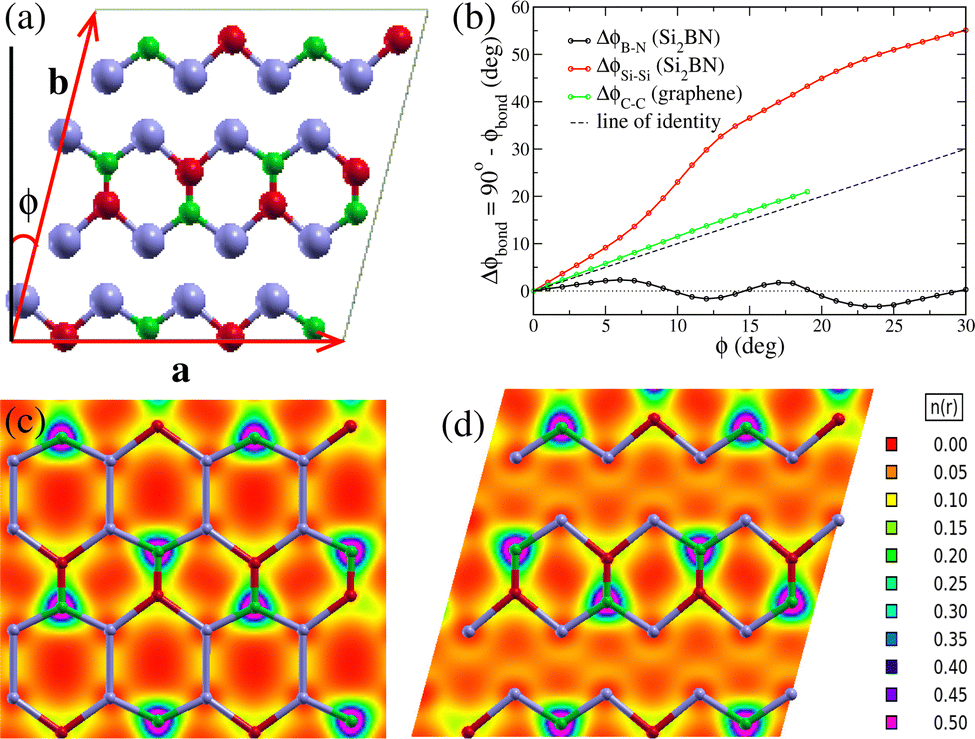 | ||
| Fig. 2 (a) Lattice vectors a and b, and the tilt angle ϕ due to shear strain. (b) The evolution with tilt angle ϕ of the angles formed between B–N and Si–Si bonds with a in Si2BN and the angle between the C–C bonds of graphene with a, which for εxy = 0 are normal to a. (c) and (d) Electron density for the unstrained AA Si2BN and for the AB Si2BN structure under shear strain for ϕ = 15°, respectively. | ||
In Fig. 3 we show the optimized structures under shear strain of Si2BN for ϕ = 0, 3°, 6°, 9°…. Below each snapshot, the tilting angle ϕ and the corresponding shear strain εxy= tanϕ are shown. As one can see, shear strain causes a relatively large tilt in the Si–Si bonds, while the direction of B–N bonds remains almost intact. This can be seen in Fig. 2(b), which shows the angle Δϕbond = 90° − ϕbond as a function of ϕ, where ϕbond is the angle between the bond direction (B–N or Si–Si) and the lattice vector a. Indeed, ΔϕB−N is very close to 0, while ΔϕSi−Si increases with ϕ, taking values well above ϕ. This figure allows us to consider that Si2BN consists of strips of hexagons containing the B–N bonds, which are interconnected through the Si–Si bonds and they slide with each other under shear strain. The bond lengths between the atoms of those stripes (i.e. the Si–B, Si–N, and B–N bond lengths) are shown in Fig. 4, where one can see that those bonds are deformed only slightly. It is worth noting that two different bonds appear between B and Si and between N and Si, which are shown in Fig. 4 as Si–N(1) and Si–N(2), and Si–B(1) and Si–B(2), respectively. From the bond length values of that figure, one can find that during the transformation from one phase to the other, the Si–N, Si–B, and B–N bonds are not shrunk by more than 3.6% and are not elongated by more than 3.0%.
 | ||
| Fig. 3 Transformation of Si2BN structure with AB stacking into Si2BN structure with AA stacking by applying shear strain. The snapshots represent the evolution of the optimized structure of AB Si2BN as shear strain increases. Below each snapshot the shear strain εxy and the tilting angle between the lattice vectors a and b are shown. Blue, red, and green spheres represent Si, B, and N atoms, respectively. | ||
 | ||
| Fig. 4 Si–B, Si–N and B–N bond lengths versus shear strain εxy. | ||
As shear strain increases, the Si–Si bond tilts are accompanied by a Si–Si bond length increase, causing bond weakening and finally bond breaking. However, before bond breaking, each Si atom of the upper strip comes closer to the next Si atom of the lower strip forming a new Si–Si bond. This can be seen in Fig. 2(c) and (d), which show the electron density for the unstrained AA Si2BN structure and the AB Si2BN under shear strain for ϕ = 15°, respectively. In the former, the electrons tend to be in the middle of the Si–Si bond, indicating covalent bonding, which however, due to the small charge density in the area between the Si atoms, is not a very strong bond. In the latter, the electron density has a small valley between the Si atoms, indicating that the electrons prefer to be closer to the Si atoms rather than in the center of the bond and the Si–Si bond starts breaking. At the same time, however, a new Si–Si bond of similar strength has started to form between the Si atom of one strip with the next Si atom of the other strip. Thus, as the shear strain increases, the former Si–Si bond breaks while the new one strengthens, replacing the former, and transforms the AB Si2BN structure into the AA one and vice versa. This bond weakening is shown in Fig. 3 as an absence of Si–Si bond sticks.
On the other hand, the corresponding snapshots for graphene, which are shown in Fig. 5, reveal a totally different behavior. In graphene, the strong C–C bonds allow only a small and uniform bond tilting which is not that large enough to cause any bond breaking. In particular, the corresponding angle ΔϕC−C for graphene, which is also shown in Fig. 2(b), almost follows the line of identity ΔϕC−C = δϕ, indicating that the bending of the C–C bonds follows the tilt angle. As εxy increases, the C–C bond lengths do not change significantly and the calculations show that the planar structure may be retained up to εxy = 0.36 (or ϕ = 20°) (see Fig. 5(a)). For larger εxy values the structure buckles to accommodate the strain, and for εxy = 0.466 (or ϕ = 25°), buckling brings closer some C atoms, (which in the unstrained structure would be far apart), which now form bonds and transform the structure into a totally new one with mixed sp1/sp2 bonding. This structure is shown in Fig. 5(c). Buckling however, may occur for even smaller εxy values and our results show that it may start at εxy ≈ 0.16 (or ϕ ≈ 10°). This result was obtained by optimizing the buckled graphene structure found for ϕ = 20°, for gradually decreasing ϕ values. According to our findings, the energy of the buckled structures is smaller than that of the planar ones for the same εxy values, and buckling disappears when ϕ drops down to ϕ = 9°. Snapshots of those buckled graphene structures are shown in Fig. 5(b).
 | ||
| Fig. 5 Snapshots of the optimized graphene structure under in-plane shear strain, (a) when planarity is retained, (b) when buckling occurs. Top and side views are shown in (b). Below each snapshot the shear strain εxy and the tilting angle between the lattice vectors a and b are shown. (c) Top view (top panel) and side view (bottom panel) of the optimized structure obtained for graphene under in-plane shear strain εxy = 0.466, corresponding to a tilting angle ϕ = 25°. The red-colored spheres represent sp1 atoms, while all other atoms are sp2. | ||
Fig. 6(a) shows the strain energy ΔE = E − E0,AB per formula unit for the Si2BN structure with respect to the energy E0,AB of the unstrained Si2BN structure with AB stacking, while Fig. 6(d) shows the corresponding one for graphene. Fig. 6(d) shows also the energy curve of Si2BN for comparison. As one can see in Fig. 6(a) the energy barrier for the transformation of Si2BN with AB stacking into the Si2BN structure with AA stacking is 0.54 eV per formula unit and corresponds to the value εxy = 0.22. This relatively small energy barrier indicates that this transformation is achievable. Considering that this process is reversible and the fact that the energy of the optimum Si2BN structure with AA stacking is smaller than Si2BN structure with AB stacking by 0.16 eV, the energy barrier for the conversion of AA into AB Si2BN is 0.70 eV per formula unit. On the other hand, the energy curve for graphene takes much higher values than those for Si2BN. It is worth noting that the energy to break the Si–Si bonds of Si2BN by applying uniaxial tensile strain along the direction of Si–Si bonds is of the order of 0.5 eV per atom.8 Considering that there is one Si–Si bond per Si2BN formula unit (four atoms), the energy to break a Si–Si bond is of the order of 2 eV.
 | ||
| Fig. 6 (a) Strain energy per formula unit ΔE, (b) shear stress σxy and (c) Si–Si interatomic distances versus shear strain εxy for the conversion of AB Si2BN into AA Si2BN. (d) Strain energy per 4-atom unit cell ΔE, (e) shear stress σxy and (f) C–C interatomic distances versus shear strain εxy for graphene. | ||
Moreover, Fig. 6(b) and (e) show the shear stress σxy for Si2BN and graphene, respectively, as a function of shear strain εxy. The stress–strain curve for Si2BN is also shown in Fig. 6(e) for comparison. As one can see, for the conversion of AB Si2BN into AA, or the opposite, the maximum shear stress that has to be applied is 11 GPa. Fitting the stress–strain curve to a cubic polynomial for ϕ in the range −5° ≤ ϕ ≤ 5° we found for Si2BN, σxy = 119.612εxy + 0.600703εxy2 − 960.050εxy3, while for graphene, σxy = 405.144εxy − 0.416954εxy2 − 318.887εxy3. Using these polynomials, one can find the shear modulus G for Si2BN and graphene, considering that for small strains G = σxy/εxy is equal to the coefficient of the linear term. Thus, for Si2BN, G = 120 GPa and for graphene G = 405 GPa. This value for graphene is consistent with the one obtained using the formula G = E/(2(1 +ν)), which is valid for isotropic materials like graphene. In this formula, E is Young's modulus, and ν the Poisson's ratio. Considering that E and ν calculated with the same method,8 are E = 964 GPa and ν = 0.190, one finds exactly the same value for G (G = E/(2(1 + ν)) = 405 GPa).
In turn, Fig. 6(c) and (d) show the evolution of the Si–Si interatomic distances d1, d2 and d3 for Si2BN, and the C–C interatomic distances d1 and d2 for graphene as a function of εxy. These interatomic distances are shown in the insets. As Fig. 6(c) shows, the bond length d1 increases as a function of εxy, while d2 and d3 decrease. For εxy = 0.27 (or ϕ ≈ 15°) the three interatomic distances become all equal and take the value d1 = d2 = d3= 2.58 Å, corresponding to an increase of the Si–Si bond length of the order of 14%. For increasing εxy values, the new Si–Si bond is formed with bond length d2 (or d3), and the structure is transformed from AB into AA Si2BN. On the other hand, Fig. 6(e) shows a totally different behavior for graphene, as already discussed above. The bond length d1 does not change significantly versus εxy, while the change in the third neighbor distance d2 is not enough to cause the breaking and the formation of new C–C bonds.
A useful practical application of the proposed phase transition would be in the field of micro-mechanical logic devices. This could be achieved by, say, assigning “0” and “1”, respectively, to AA and AB stacking. A key benefit of this is that Si2BN based systems can be used to store data by means of mechanical applications without requiring electric power. Other applications may be considered by exploiting the practically infinite shear ductility of the structure (since the structural features are retained) either in the AA or AB stacking.
In conclusion, using first-principles calculations, we report the existence of an unusual phase transition in the novel Si2BN 2D material, transforming Si2BN with AB stacking into Si2BN with AA stacking and vice versa. This is demonstrated via the application of in-plane shear strain which, contrary to other 2D materials, causes no buckling at any stage of the transformation process.
Author contributions
ZGF: conceptualization, data curation, formal analysis, investigation, methodology, project administration, software, resources, supervision, validation, visualization, writing – original draft. MM: conceptualization, methodology, project administration, supervision, validation, visualization, writing – review & editing.Data availability
All data that support the findings of this study are included in the article.Conflicts of interest
There are no conflicts to declare.Acknowledgements
ZGF wishes to acknowledge financial support from (i) the LESGO H2020-EIC-FETPROACT 2019–2020 project (agreement no. 952068) of the European Union and (ii) the project PRIN 2022 – Cod. 202278NHAM (PE11) CHERICH-C “Chemical and electrochemical energy storage materials from organic wastes: the treasure hidden in C-based materials” – CUP B53D23008590006, funded by the European Union – Next Generation EU in the context of the Italian National Recovery and Resilience Plan, Mission 4, Component 2, Investment 1.1, “Fondo per il Programma Nazionale di Ricerca e Progetti di Rilevante Interesse Nazionale (PRIN)”.Notes and references
- A. N. Andriotis, E. Richter and M. Menon, Phys. Rev. B, 2016, 93, 081413 CrossRef.
- E. D. Sandoval, S. Hajinazar and A. N. Kolmogorov, Phys. Rev. B, 2016, 94, 094105 CrossRef.
- Z. G. Fthenakis, M. Jaishi, B. Narayanan, A. N. Andriotis and M. Menon, J. Phys.: Condens. Matter., 2021, 33, 165001 CrossRef CAS PubMed.
- J. P. Perdew, K. Burke and M. Ernzerhof, Phys. Rev. Lett., 1996, 77, 3865–3868 CrossRef CAS PubMed.
- J. M. Soler, E. Artacho, J. D. Gale, A. García, J. Junquera, P. Ordejón and D. Sánchez-Portal, J. Phys.: Condens. Matter., 2002, 14, 2745 CrossRef CAS.
- H. R. Mahida, D. Singh, Y. Sonvane, P. B. Thakor, R. Ahuja and S. K. Gupta, J. App. Phys., 2019, 126, 233104 CrossRef.
- C.-W. Wu, C. Xiang, H. Yang, W.-X. Zhou, G. Xie, B. Ou and D. Wu, Chin. Phys. B, 2021, 30, 037304 CrossRef CAS.
- Z. G. Fthenakis and M. Menon, Phys. Rev. B, 2019, 99, 205302 CrossRef CAS.
- S. Hu, Y. Yong, C. Li, Z. Zhao, H. Jia and Y. Kuang, Phys. Chem. Chem. Phys., 2020, 22, 13563–13568 RSC.
- A. M. Satawara, G. A. Shaikh, S. K. Gupta, A. N. Andriotis, M. Menon and P. Gajjar, Int. J. Hydrogen Energy, 2023, 48, 25438–25449 CrossRef CAS.
- M. Jiang, J. Xu, P. Munroe, Z.-H. Xie and Z. Chen, Int. J. Hydrogen Energy, 2023, 50, 865–878 CrossRef.
- R. Akilan, D. Ravichandran, S. Vinnarasi and R. Shankar, Mater. Lett., 2020, 279, 128487 CrossRef CAS.
- P. Panigrahi, Y. Pal, R. Ahuja and T. Hussain, Energy Fuels, 2021, 35, 12688–12699 CrossRef CAS.
- P. Panigrahi, S. B. Mishra, T. Hussain, B. R. K. Nanda and R. Ahuja, ACS Appl. Nano Mater., 2020, 3, 9055–9063 CrossRef CAS.
- V. Babar, A. Murat and U. Schwingenschlögl, J. Phys.: Cond. Matter., 2020, 32, 355602 CrossRef CAS PubMed.
- S. Thomas, A. K. Madam and M. Asle Zaeem, Phys. Chem. Chem. Phys., 2022, 24, 4394–4406 RSC.
- D. Singh, S. Chakraborty and R. Ahuja, ACS Appl. Energy Mater., 2019, 2, 8441–8448 CrossRef CAS.
- D. S. Akilesh Muralidharan, M. Subramani and S. Ramasamy, J. Biomol. Struct. Dyn., 2023, 0, 1–32 Search PubMed.
- K. G. Reeves, Y. Yao and Y. Kanai, J. Chem. Phys., 2016, 145, 124705 CrossRef PubMed.
- J. Zhou and S. Zhang, npj 2D Mater. Appl., 2021, 5, 16 CrossRef CAS.
- J. Zhou, S. Zhang and J. Li, NPG Asia Mater., 2020, 12, 2 CrossRef CAS.
- N. Troullier and J. L. Martins, Phys. Rev. B: Condens. Matter Mater. Phys., 1991, 43, 1993–2006 CrossRef CAS PubMed.
- L. Kleinman and D. M. Bylander, Phys. Rev. Lett., 1982, 48, 1425–1428 CrossRef CAS.
- H. J. Monkhorst and J. D. Pack, Phys. Rev. B, 1976, 13, 5188–5192 CrossRef.
- Z. G. Fthenakis and N. N. Lathiotakis, Phys. Chem. Chem. Phys., 2015, 17, 16418–16427 RSC.
| This journal is © the Owner Societies 2025 |