Tunnel barriers for Fe-based spin valves providing high spin-polarized current
Received
29th October 2024
, Accepted 4th December 2024
First published on 15th January 2025
Abstract
Employing density functional theory for ground state quantum mechanical calculations and the non-equilibrium Green's function method for transport calculations, we investigate the potential of CdS, ZnS, Cd3ZnS4, and Zn3CdS4 as tunnel barriers in magnetic tunnel junctions for spintronics. Based on the finding that the valence band edges of these semiconductors are dominated by pz orbitals and the conduction band edges by s orbitals, we show that Δ1 symmetry filtering of the Bloch states in magnetic tunnel junctions with Fe electrodes results in high tunneling magnetoresistances and high spin-polarized current (up to two orders of magnitude higher than in the case of the Fe/MgO/Fe magnetic tunnel junction).
I. Introduction
The resistance of an anisotropic magnetoresistance (AMR) device depends on the angle between the electric current and the external magnetic field, being minimal/maximal for perpendicular/parallel orientation.1 The resistance of a giant magnetoresistance (GMR) device, consisting of a non-magnetic metal (such as Cu and Pt) sandwiched between ferromagnetic electrodes, depends on the relative orientation of the magnetic moments of the electrodes, being minimal/maximal for parallel/antiparallel P/AP orientation.2,3 In a tunneling magnetoresistance (TMR) device the non-magnetic metal is replaced with an insulator.4 Coherent tunneling through a crystalline barrier results in| |  | (1) |
where TP/TAP is the transmission for P/AP orientation of the magnetic moments of the electrodes, while incoherent tunneling through an amorphous barrier results in| |  | (2) |
where PL/PR is the density of states at the Fermi energy (EF) of the left/right electrode.5 In the case of coherent tunneling in an epitaxial junction the transverse component k‖ of the wave vector k is conserved. The resistance depends not only on the relative orientation of the magnetic moments of the electrodes but also on the orbital angular momentum symmetry of the wave function of the tunneling electrons. While various junctions6–8 realize such symmetry filtering, only the combination of a MgO barrier with Fe electrodes is adopted in main-stream applications, mainly because boron assisted epitaxial growth is used to minimize spin flip and interband scattering.9,10
Achieving a high spin-polarized current is paramount for magnetic random access memories in that switching between the magnetic configurations storing binary information is achieved by spin transfer torque,11–13 because the spin transfer torque is proportional to the generating spin-polarized current.14,15 The same applies, for example, to magnetic flip–flops in that the magnetic state is switched by spin-polarized current.16,17 As it is vital to identify magnetic tunnel junctions (MTJs) based on semiconductors that can be integrated with the current lithographic processes to open new avenues for spintronics, we present here a detailed theoretical analysis of potential barrier materials with zinc blende crystal structure (CdS, ZnS, Cd3ZnS4, and Zn3CdS4) that are extensively used industrially in light emitting diodes.18–20 For the electrodes we use Fe as strong ferromagnet with high Curie temperature.21 The bcc structure of Fe shares with the zinc blende structure the 4-fold rotation symmetry about the [001] direction, enabling growth of a MTJ by chemical vapor deposition and molecular beam epitaxy. Being II–VI compounds with direct band gaps, CdS and ZnS are also applied as transparent semiconductors22,23 and for photocatalysis.24,25 The excitonic properties, particularly the binding energy, can be tuned well by doping.26 High quantum transport is possible due to dispersive bands with small electron effective masses of 0.18m0 (CdS)27 and 0.34m0 (ZnS),28 where m0 is the free electron mass.
After introducing our computational methodology, we will analyze the properties of Fe/CdS/Fe, Fe/ZnS/Fe, Fe/Cd3ZnS4/Fe, and Fe/Zn3CdS4/Fe MTJs based on the real and complex band structures of the barrier and electrode materials, to prepare for a detailed discussion of the transmission and TMR. A summary of the main findings is provided in the conclusion section.
II. Computational details
The ground state electronic properties of CdS, ZnS, Cd3ZnS4, and Zn3CdS4 are obtained from Kohn–Sham density functional theory using the SIESTA engine29 with non-relativistic norm-conserving Troullier–Martins pseudopotentials and localized atomic orbitals as basis set. The exchange–correlation functional is treated in the Ceperley–Alder parametrization of the local density approximation. Double-ζ basis functions are used for the s, p, and d orbitals of Fe, Cd, and Zn, while double-ζ plus polarization basis functions are used for the s and p orbitals of S. The atomic self-interaction correction (ASIC) is employed to correct the band gaps.30,31 We use a grid spacing equivalent to a plane wave cutoff of 400 Ry and a Monkhorst–Pack 8 × 8 × 8 k-point mesh. Complex band structures are obtained through the secular equation for k‖ = 0.
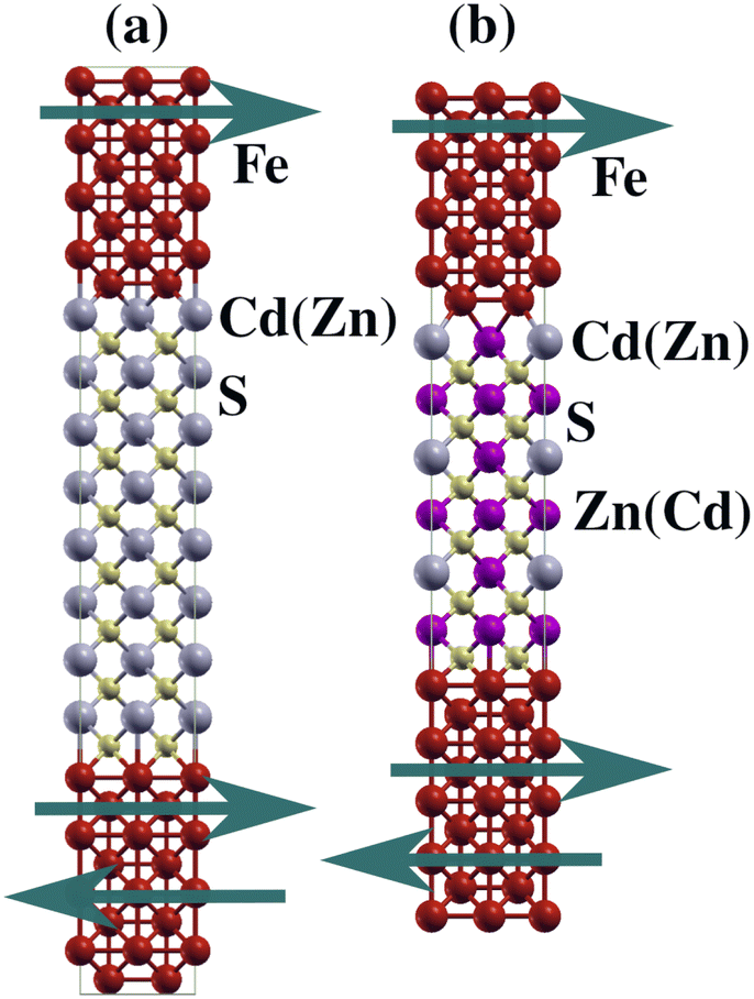
The experimental lattice parameters of zinc blende CdS and ZnS are 5.83 Å32 and 5.41 Å,33 respectively, and the optimized lattice parameters of Cd3ZnS4 and Zn3CdS4 are found to be 5.76 Å and 5.51 Å. We use a 2 × 2 supercell of body-centered cubic Fe to create MTJs and absorb the lattice mismatch by altering the lattice parameter of Fe (experimental value: 2.86 Å34), which hardly modifies the electronic properties. The thickness of the barrier material is chosen as 26.75 Å (3 unit cells), 40.24 Å (7 unit cells), 20.69 Å (3 unit cells), and 19.79 Å (3 unit cells) for CdS, ZnS, Cd3ZnS4, and Zn3CdS4, respectively. Due to the larger band gap of ZnS an increased thickness is chosen to enhance the TMR. The atomic positions in the MTJs (inequivalent interfaces, see Fig. 1) are relaxed by the conjugate gradient method until all atomic forces stay below 0.01 eV Å−1.
 |
| | Fig. 1 Scattering regions of the (a) Fe/CdS/Fe (Fe/ZnS/Fe) and (b) Fe/Cd3ZnS4/Fe (Fe/Zn3CdS4/Fe) MTJs. The arrows represent the magnetic moments of the two Fe electrodes, which can be oriented parallel or antiparallel. Color code: Fe = red; Cd = grey; Zn = magenta; S = yellow. | |
The SMEAGOL engine,35–37 which is interfaced with the SIESTA engine, is used to execute non-equilibrium Green's function transport calculations. In this formalism the complex self-energy
| |  | (3) |
where
σ = ↑/↓ is the spin,
Hσλ(
E,
V) is the coupling Hamiltonian between the electrode and scattering region,
gσλ(
E,
V) is the surface Green's function of the electrode, and
λ = L/R denotes the left/right electrode, is added to the Hamiltonian
HσC(
E,
V) of the scattering region to obtain the effective Green's function
| |  | (4) |
GσC(
E,
V) is finite and Hermitian with density matrix
| |  | (5) |
where
| |  | (6) |
is the lesser Green's function,
fσλ(
E,
V) is the Fermi–Dirac distribution function, and
| |  | (7) |
is the coupling matrix between the electrode and scattering region (retarded/advanced part of the self-energy denoted by superscript +/−).
Using the spin-dependent transmission
| |  | (8) |
the S
MEAGOL engine calculates the voltage-dependent spin-polarized current in the Landauer–Büttiker formalism as
| | 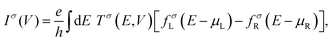 | (9) |
where
e is the electron charge,
h is the Planck constant, and
μL/R =
EF ±
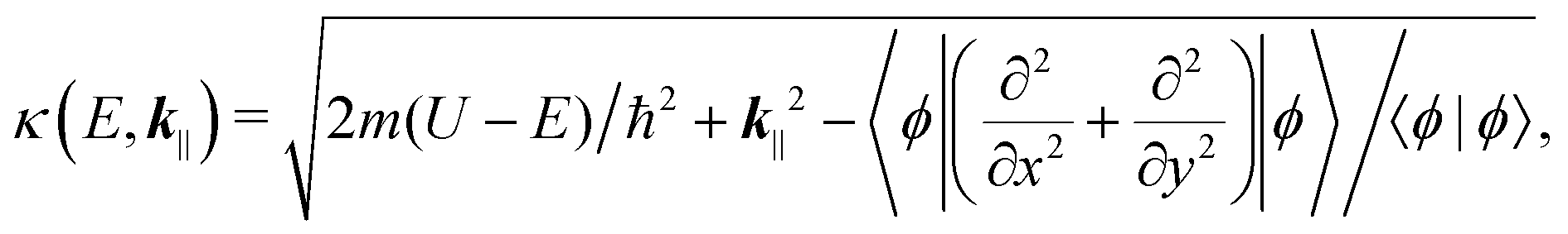
eV/2 is the chemical potential. In the barrier the normal component of the wave vector becomes complex,
k⊥(
E,
k‖) =
iκ(
E,
k‖), with
| |  | (10) |
where
m is the effective mass,
U is the barrier height, and the last term takes into account that the decay in the barrier is stronger when the transverse angular momentum of the wave function is higher. Since the junction is translationally invariant in the transverse plane, we can write
| |  | (11) |
where
ΩBZ is the volume of the two-dimensional Brillouin zone (BZ), the
k‖-dependent transmission

is determined by the atomic composition and structure of the junction, and
d is the thickness of the barrier. We calculate
T(
E) =
T↑(
E, 0) +
T↓(
E, 0) for both the P and AP orientations to obtain the TMR through
eqn (1). The transport calculations are performed after converging the charge density matrix with a tolerance of 10
−4e. We show in the following results obtained for a 50 × 50 × 1
k-point mesh, while no relevant change is observed in test calculations for a 100 × 100 × 1
k-point mesh.
III. Results and discussion
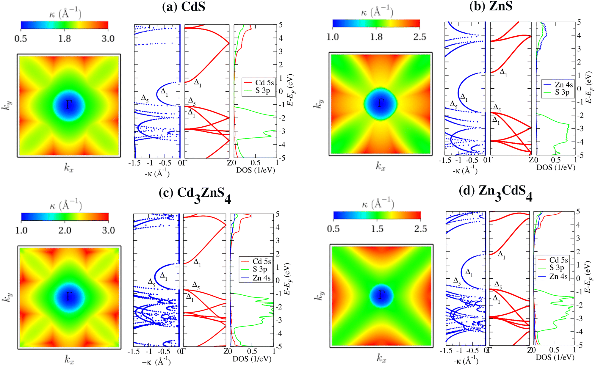
While the experimental band gaps of CdS and ZnS are 2.6 eV24 and 3.7 eV,22 respectively, we obtain appropriate ASIC values of 1.9 eV and 3.0 eV. For Cd3ZnS4 and Zn3CdS4 we obtain ASIC band gaps of 2.0 eV and 2.5 eV, respectively. Note that the size of the band gap scales  but does not change its distribution in the BZ. The heat maps of κ(EF, k‖) in Fig. 2 show a four-fold rotation symmetry. Mainly the regions around the Γ-point and along the diagonals of the BZ contribute to Tσ(EF, V) due to low values of κ(EF, k‖), which also turns out to be true for E ≠ EF. As the tunneling electrons experience minimal κ(E, k‖) at the Γ-point, that is, when they approach the barrier in the normal direction (minimal effective barrier thickness), the following analysis focusses on the Γ-point. However, note that this provides only a qualitative picture, because Tσ(E, V), while being dominated by the Γ-point, generally depends on the entire BZ. Tσ(E, V) of the MTJ will be high (and therefore the current will be high) if the symmetries of the Bloch states at EF in the electrodes and at the band edges in the barrier are the same, and a high TMR is expected if only one spin channel (either majority or minority) is present in the ferromagnetic electrodes. The absence of an abrupt change in the Hartree potential at the interface of an epitaxial junction results in a weak Rashba field, which minimizes the spin flip and interband scatterings to assist coherent quantum tunneling.
 |
| | Fig. 2 Electronic structure analysis of (a) CdS, (b) ZnS, (c) Cd3ZnS4, and (d) Zn3CdS4. The left panels show heat maps (from the minimal to the maximal value on a linear scale) of κ(EF, k‖) in the BZ, the middle panels show the real (red) and complex (blue) band structures, and the right panels show the partial densities of states. | |
According to Fig. 2, the four barrier materials under investigation exhibit direct band gaps and similar band dispersions along Γ–Z. No complex ghost bands due to the non-orthogonal orbital basis set are observed.38 The valence band edges are dominated by pz orbitals and the conduction band edges are dominated by s orbitals. These orbitals couple with the Bloch states of the electrodes. The symmetry Δ of a Bloch state is assigned by projecting the wavefunction to the atomic orbitals and analyzing the angular momentum along the transport direction. The s, pz, and d3z2−r2 orbitals have zero angular momentum along the transport direction and thus map to Δ1 symmetry. Similarly, the px, py, dxz, and dyz orbitals map to Δ5 symmetry, the dxy orbital maps to  symmetry, and the dx2−y2 orbital maps to Δ2 symmetry. The results of the symmetry assignment are shown in Fig. 2. Analysis of the complex band structures in Fig. 2 at the Γ-point suggests that all four barrier materials filter Bloch states of Δ1 symmetry. In each case, a complex band of Δ1 symmetry smoothly connects the valence band maximum to the conduction band minimum. On the other hand, the complex band of Δ5 symmetry present at the valence band edge connects to deep inside the conduction band and thus hardly contributes to Tσ(E, V), unless EF of the MTJ is pinned close to valence band edge (implying that hopping dominates over tunneling and the MTJ behaves like a GMR device).
In the case of the epitaxial Fe/MgO/Fe MTJ the Δ1-symmetric majority spin states of Fe match exactly with the Δ1-symmetric states forming the valence and conduction band edges of MgO (at the Γ-point), resulting in a high TMR of ∼10![[thin space (1/6-em)]](https://www.rsc.org/images/entities/char_2009.gif) 000%.39,40 The band structure of body-centered cubic Fe along Γ–Z is shown in Fig. 3 together with heat maps of the numbers of majority and minority spin channels in the BZ (reflecting the four-fold rotation symmetry of the body-centered cubic structure). Both the majority and minority spin channels are concentrated around the Γ-point. A majority spin Δ1 band crosses EF with high dispersion, while the corresponding minority spin Δ1 band appears at higher energy due to the magnetic exchange field, resulting in 100% spin polarization in the Δ1 channel. The Δ2 and Δ5 bands crossing EF give only small contributions to Tσ(E, V) due to mismatch with the Bloch state symmetry of the barrier (Δ1).
000%.39,40 The band structure of body-centered cubic Fe along Γ–Z is shown in Fig. 3 together with heat maps of the numbers of majority and minority spin channels in the BZ (reflecting the four-fold rotation symmetry of the body-centered cubic structure). Both the majority and minority spin channels are concentrated around the Γ-point. A majority spin Δ1 band crosses EF with high dispersion, while the corresponding minority spin Δ1 band appears at higher energy due to the magnetic exchange field, resulting in 100% spin polarization in the Δ1 channel. The Δ2 and Δ5 bands crossing EF give only small contributions to Tσ(E, V) due to mismatch with the Bloch state symmetry of the barrier (Δ1).
 |
| | Fig. 3 (a) Real band structure with the Bloch state symmetry indicated and (b) numbers of majority and minority spin channels in the BZ (simulation cell with 16 atoms) of body-centered cubic Fe. | |
Fig. 4 shows T(E) for both the P and AP configurations separately for the majority and minority spin channels. The obtained dominant symmetries of the two spin channels at the Γ-point are summarized in Table 1. The Fe/CdS/Fe MTJ shows in the P configuration almost pure majority spin transmission in the range −1.5 eV < E − EF < −0.5 eV. At EF the TMR is 30% and at EF + 0.1 eV the highest TMR of 5000% is obtained. The Fe/ZnS/Fe MTJ shows in both the P and AP configurations almost pure majority spin transmission in the range −2.4 eV < E − EF < −1.1 eV and in the P (AP) configuration almost pure majority (minority) spin transmission in the range −0.1 eV < E − EF < 0.6. At EF the TMR is 10% and at EF − 2.0 eV the highest TMR of 600% is obtained. The Fe/Cd3ZnS4/Fe MTJ shows in the P configuration almost pure majority spin transmission in the range −0.5 eV < E − EF < 0.0 eV. At EF the TMR is 40% and at EF − 0.9 eV the highest TMR of 1000% is obtained. The Zn3CdS4 MTJ shows in the P configuration almost pure majority spin transmission in the range −2.0 eV < E − EF < −1.0 eV, in the AP configuration almost pure minority spin transmission in the range −1.0 eV < E − EF < −0.5 eV, and in both the P and AP configurations almost pure majority spin transmission in the range 0.0 eV < E − EF < 0.3 eV. At EF the TMR is 110% and at EF − 1.5 eV the highest TMR of 600% is obtained.
 |
| | Fig. 4 Zero-bias transmission and TMR of the (a) Fe/CdS/Fe, (b) Fe/ZnS/Fe, (c) Fe/Cd3ZnS4/Fe, and (d) Fe/Zn3CdS4/Fe MTJs as functions of energy. | |
Table 1 Symmetry analysis
| MTJ |
Configuration |
Energy range (E − EF) |
Dominant symmetry of majority spin channel |
Dominant symmetry of minority spin channel |
| Fe/CdS/Fe |
P |
−3.0 eV to −0.5 eV |
Δ
1, Δ2, Δ5 |
Δ
1, Δ2 |
| P |
+0.0 eV to +1.0 eV |
Δ
1
|
Δ
2, Δ5 |
| P |
+1.0 eV to +2.1 eV |
Δ
1
|
Δ
1, Δ2, Δ5 |
| Fe/CdS/Fe |
AP |
−1.7 eV to −1.5 eV |
Δ
2, Δ5 |
Δ
2
|
| AP |
−1.3 eV to −0.5 eV |
Δ
1, Δ2, Δ5 |
Δ
2
|
| Fe/ZnS/Fe |
P |
−2.4 eV to −0.3 eV |
Δ
1, Δ2, Δ5 |
Δ
2
|
| P |
−0.1 eV to +0.6 eV |
Δ
1, Δ5 |
Δ
2, Δ5 |
| Fe/ZnS/Fe |
AP |
−2.4 eV to −1.1 eV |
Δ
2, Δ5 |
Δ
2
|
| AP |
−1.0 eV to +0.6 eV |
Δ
1, Δ5 |
Δ
2, Δ5 |
| Fe/Cd3ZnS4/Fe |
P |
−3.0 eV to −0.7 eV |
Δ
1, Δ2, Δ5 |
Δ
1, Δ2 |
| P |
−0.5 eV to +0.0 eV |
Δ
1, Δ5 |
Δ
2, Δ5 |
| P |
+0.7 eV to +1.0 eV |
Δ
1
|
Δ
2, Δ5 |
| P |
+1.0 eV to +2.0 eV |
Δ
1
|
Δ
1, Δ2, Δ5 |
| Fe/Cd3ZnS4/Fe |
AP |
−1.0 eV to −0.3 eV |
Δ
1, Δ5 |
Δ
2, Δ5 |
| AP |
−0.2 eV to +0.3 eV |
Δ
1, Δ5 |
Δ
2, Δ5 |
| AP |
+0.3 eV to +0.6 eV |
Δ
1
|
Δ
2, Δ5 |
| AP |
+1.3 eV to +1.9 eV |
Δ
1
|
Δ
1, Δ2, Δ5 |
| Fe/Zn3CdS4/Fe |
P |
−2.0 eV to −1.0 eV |
Δ
1, Δ2, Δ5 |
Δ
2
|
| P |
−1.0 eV to +0.0 eV |
Δ
1, Δ2, Δ5 |
Δ
2, Δ5 |
| Fe/Zn3CdS4/Fe |
AP |
−1.0 eV to −0.5 eV |
Δ
1, Δ5 |
Δ
2
|
| AP |
−0.5 eV to +0.3 eV |
Δ
1, Δ5 |
Δ
2, Δ5 |
The spin-polarized current I↑ − I↓ is shown in Fig. 5 for both the P and AP configurations in comparison to that of a Fe/MgO/Fe MTJ with a barrier thickness of 15.44 Å. At V = 2 V, for example, the spin-polarized current density of the P configuration amounts to 3.0 × 10⁸ A cm−2 for the Fe/CdS/Fe MTJ, 6.0 × 10⁶ A cm−2 for the Fe/ZnS/Fe MTJ, 4.4 × 10⁸ A cm−2 for the Fe/Cd3ZnS4/Fe MTJ, and 5.0 × 10⁷ A cm−2 for the Fe/Zn3CdS4/Fe MTJ, exceeding the value of 2.4 × 10⁶ A cm−2 obtained for the Fe/MgO/Fe MTJ by up to two orders of magnitude. The bias-dependence of the transmission of the Fe/Cd3ZnS4/Fe MTJ with the highest spin-polarized current density of the P configuration is shown in Fig. 6.
 |
| | Fig. 5 Spin-polarized current in the (a) P and (b) AP configurations. | |
 |
| | Fig. 6 Bias-dependence of the transmission of the Fe/Cd3ZnS4/Fe MTJ in the P configuration. | |
IV. Conclusion
We have explored the possibility of using the opto-electronic materials CdS, ZnS, Cd3ZnS4, and Zn3CdS4 as tunnel barriers in next generation MTJs. Fe-based MTJs adopting these semiconductors are found to have excellent potential in hybrid memory/logic components, displays with large viewing angle, and quantum-bit manipulators, for example, due to the provided high spin-polarized current. We have identified the areas of the two-dimensional BZ where κ(EF, k‖) is minimal and T(EF) therefore is maximal, finding in each case dominant transport at the Γ-point, where the valence band edges are dominated by pz orbitals and the conduction band edges are dominated by s orbitals. By complex band analysis we have established Δ1 symmetry filtering of the Bloch states at the Γ-point. The highest TMR is found to be 5000% at EF + 0.1 eV for the Fe/CdS/Fe MTJ, 600% at EF − 2.0 eV for the Fe/ZnS/Fe MTJ, 1000% at EF − 0.9 eV for the Fe/Cd3ZnS4/Fe MTJ, and 600% at EF − 1.5 eV for the Fe/Zn3CdS4/Fe MTJ.
Data availability
The article includes all the data generated in this study.
Conflicts of interest
There are no conflicts to declare.
Acknowledgements
The research reported in this publication was supported by funding from King Abdullah University of Science and Technology.
References
-
A. B. Pippard, Magnetoresistance in metals, Cambridge University Press, Cambridge, 1989 Search PubMed.
- M. N. Baibich, J. M. Broto, A. Fert, F. N. Van Dau, F. Petroff, P. Eitene, G. Greuzet, A. Friederich and J. Chazelas, Giant magnetoresistance of (001)Fe/(001)Cr magnetic superlattices, Phys. Rev. Lett., 1998, 64, 2472 Search PubMed.
- G. Binasch, P. Grünberg, F. Saurenbach and W. Zinn, Enhanced magnetoresistance in layered magnetic structures with antiferromagnetic interlayer exchange, Phys. Rev. B: Condens. Matter Mater. Phys., 1989, 39, 4828 CrossRef CAS PubMed.
- F. J. Gregg, I. Petej, E. Jouguelet and C. Dennis, Spin electronics – A review, J. Phys. Appl. Phys., 2002, 35, R121 CrossRef.
- M. Julliere, Tunneling between ferromagnetic films, Phys. Lett. A, 1975, 54, 225 CrossRef.
- H. X. Liu, Y. Honda, T. Taira, K. I. Matsuda, M. Arita, T. Uemura and M. Yamamoto, Giant tunneling magnetoresistance in epitaxial Co2MnSi/MgO/Co2MnSi magnetic tunnel junctions by half-metallicity of Co2MnSi and coherent tunneling, Appl. Phys. Lett., 2012, 101, 132418 CrossRef.
- S. V. Faleev, S. S. P. Parkin and O. N. Mryasov, Brillouin zone spin filtering mechanism of enhanced tunneling magnetoresistance and correlation effects in a Co(0001)/h-BN/Co(0001) magnetic tunnel junction, Phys. Rev. B: Condens. Matter Mater. Phys., 2015, 92, 235118 CrossRef.
- G. Shukla, T. Archer and S. Sanvito, HfO2 and SiO2 as barriers in magnetic tunneling junctions, Phys. Rev. B, 2017, 95, 184410 CrossRef.
- S. S. P. Parkin, C. Kaiser, A. Panchula, P. M. Rice, B. Hughes, M. Samant and S. H. Yang, Giant tunnelling magnetoresistance at room temperature with MgO(100) tunnel barriers, Nat. Mater., 2004, 3, 862 CrossRef CAS PubMed.
- S. Yuasa, T. Nagahama, A. Fukushima, Y. Suzuki and K. Ando, Giant room-temperature magnetoresistance in single-crystal Fe/MgO/Fe magnetic tunnel junctions, Nat. Mater., 2004, 3, 868 CrossRef CAS PubMed.
- S. Bhatti, R. Sbiaa, A. Hirohata, H. Ohno, S. Fukami and S. N. Piramanayagam, Spintronics based random access memory: A review, Mater. Today, 2017, 20, 530 CrossRef.
- C. Safranski, J. Z. Sun and A. D. Kent, A perspective on electrical generation of spin current for magnetic random access memories, Appl. Phys. Lett., 2022, 120, 160502 CrossRef CAS.
- C. P. Wang, S. H. Cheng and W. J. Hsue, High spin current density in gate-tunable spin-valves based on graphene nanoribbons, Sci. Rep., 2023, 13, 9234 CrossRef CAS PubMed.
- T. Yang, J. Hamrle, T. Kimura and Y. Otani, Roles of spin-polarized current and spin accumulation in the current-induced magnetization switching, J. Magn. Magn. Mater., 2006, 301, 389 CrossRef CAS.
- D. C. Ralph and M. D. Stiles, Spin transfer torques, J. Magn. Magn. Mater., 2008, 320, 1190 CrossRef CAS.
- H. Cai, Y. Wang, L. Alves De Barros Naviner and W. Zhao, Low power magnetic flip-flop optimization with FDSOI technology boost, IEEE Trans. Magn., 2016, 52, 3401807 Search PubMed.
- Z. Wang, L. Zhang, M. Wang, Z. Wang, D. Zhu, Y. Zhang and W. Zhao, High-density NAND-like spin transfer torque memory with spin-orbit torque erase operation, IEEE Electron Device Lett., 2018, 39, 343 CAS.
- B. O. Dabbousi, J. Rodriguez-Viejo, F. V. Mikulec, J. R. Heine, H. Mattoussi, R. Ober, K. F. Jensen and M. G. Bawendi, (CdSe)ZnS core-shell quantum dots: Synthesis and characterization of a size series of highly luminescent nanocrystallites, J. Phys. Chem. B, 1997, 101, 9463 CrossRef CAS.
- R. Fiederling, M. Keim, G. Reuscher, W. Ossau, G. Schmidt, A. Waag and L. W. Molenkamp, Injection and detection of a spin polarized current in a light-emitting diode, Nature, 1999, 402, 787 CrossRef.
- M. Holub and P. Bhattacharya, Spin-polarized light-emitting diodes and lasers, J. Phys. D: Appl. Phys., 2007, 40, R179 CrossRef CAS.
-
E. Y. Tsymbal and I. Zutic, Handbook of spin transport and magnetism, CRC Press, Boca Raton, 2011 Search PubMed.
- S. R. Chalana, V. Ganesan and V. P. Mahadevan Pillai, Surface plasmon resonance in nanostructured Ag incorporated ZnS films, AIP Adv., 2015, 5, 107207 CrossRef.
- S. Kim, J. Suh, T. Kim, J. Hong and S. Cho, Plasmon-enhanced performance of CdS/CdTe solar cells using Au nanoparticles, Opt. Express, 2019, 27, 22018 Search PubMed.
- N. E. Fard, R. Fazaeli and R. Ghiasi, Band gap energies and photocatalytic properties of CdS and Ag/CdS nanoparticles for azo dye degradation, Chem. Eng. Technol., 2016, 39, 149 CrossRef.
- Y. J. Yuan, D. Chen, Z. T. Yu and Z. G. Zou, Cadmium sulfide-based nanomaterials for photocatalytic hydrogen production, J. Mater. Chem. A, 2018, 6, 11606 RSC.
- W. Wu, W. Liu, Q. Han, Y. Gao, D. Kong and Q. Yang, Composition effect on exciton recombination dynamics of blue-emitting alloyed Cd1−xZnxS/ZnS quantum dots, J. Mater. Chem. C, 2023, 11, 1854 RSC.
- B. Podor, J. Balazs and M. Harsy, Electron concentration and mobility in CdS single crystal, Phys. Status Solidi A, 1971, 8, 613 CrossRef CAS.
- C. G. Rodrigues, Electron mobility in n-doped zinc sulphide, Microelectron. J., 2006, 37, 657 CrossRef CAS.
- J. M. Soler, E. Artacho, J. D. Gale, A. Garcia, J. Junquera, P. Ordejón and D. Sánchez-Portal, The SIESTA method for ab initio order-N materials simulation, J. Phys.: Condens. Matter, 2002, 14, 2745 CrossRef CAS.
- C. D. Pemmaraju, T. Archer, D. Sánchez-Portal and S. Sanvito, Atomic-orbital-based approximate self-interaction correction scheme for molecules and solids, Phys. Rev. B: Condens. Matter Mater. Phys., 2007, 75, 045101 CrossRef.
- A. Filippetti, C. D. Pemmaraju, S. Sanvito, P. Delugas, D. Puggioni and V. Fiorentini, Variational pseudo-self-interaction-corrected density functional approach to the ab initio description of correlated solids and molecules, Phys. Rev. B: Condens. Matter Mater. Phys., 2011, 84, 195127 CrossRef.
- A. A. I. Al-Bassam, A. A. Al-Juffali and A. M. Al-Dhafir, Structure and lattice parameters of cadmium suiphide selenide (CdSxSe1−x) mixed crystals, J. Crystallogr., 1994, 135, 476 CAS.
-
S. Adachi, Cubic Zinc sulphide (β-ZnS): Optical constants of crystalline and amorphous semiconductors, Springer, Boston, 1999, pp. 445–458 Search PubMed.
- Y. I. Petrov, E. A. Shafranovsky, Y. F. Krupyanskii and S. V. Essine, Structure and Mössbauer spectra for the Fe-Cr system: From bulk alloy to nanoparticles, J. Appl. Phys., 2002, 91, 352 CrossRef CAS.
- A. R. Rocha, V. M. García-Suárez, S. Bailey, C. J. Lambert, J. Ferrer and S. Sanvito, Towards molecular spintronics, Nat. Mater., 2005, 4, 335 CrossRef CAS PubMed.
- A. R. Rocha, V. M. García-Suárez, S. Bailey, C. J. Lambert, J. Ferrer and S. Sanvito, Spin and molecular electronics in atomically generated orbital landscapes, Phys. Rev. B: Condens. Matter Mater. Phys., 2006, 73, 085414 CrossRef.
- I. Rungger and S. Sanvito, Algorithm for the construction of self-energies for electronic transport calculations based on singularity elimination and singular value decomposition, Phys. Rev. B: Condens. Matter Mater. Phys., 2008, 78, 035407 CrossRef.
- F. Sacconi, J. M. Jancu and M. Povolotskyi, and A. Di Carlo, Full-band tunneling in high-κ oxide MOS structures, IEEE Trans. Electron Devices, 2007, 54, 3168 CAS.
- W. H. Butler, X. G. Zhang, T. C. Schulthess and J. M. Maclaren, Spin-dependent tunneling conductance of Fe/MgO/Fe sandwiches, Phys. Rev. B: Condens. Matter Mater. Phys., 2001, 63, 054416 CrossRef.
- J. Mathon and A. Umerski, Theory of tunneling magnetoresistance of an epitaxial Fe/MgO/Fe(001) junction, Phys. Rev. B: Condens. Matter Mater. Phys., 2001, 63, 220403 CrossRef.
|
| This journal is © the Owner Societies 2025 |
Click here to see how this site uses Cookies. View our privacy policy here. 
 Open Access Article
 This Open Access Article is licensed under a Creative Commons Attribution-Non Commercial 3.0 Unported Licence
 *
*


 is determined by the atomic composition and structure of the junction, and d is the thickness of the barrier. We calculate T(E) = T↑(E, 0) + T↓(E, 0) for both the P and AP orientations to obtain the TMR through eqn (1). The transport calculations are performed after converging the charge density matrix with a tolerance of 10−4e. We show in the following results obtained for a 50 × 50 × 1 k-point mesh, while no relevant change is observed in test calculations for a 100 × 100 × 1 k-point mesh.
 but does not change its distribution in the BZ. The heat maps of κ(EF, k‖) in Fig. 2 show a four-fold rotation symmetry. Mainly the regions around the Γ-point and along the diagonals of the BZ contribute to Tσ(EF, V) due to low values of κ(EF, k‖), which also turns out to be true for E ≠ EF. As the tunneling electrons experience minimal κ(E, k‖) at the Γ-point, that is, when they approach the barrier in the normal direction (minimal effective barrier thickness), the following analysis focusses on the Γ-point. However, note that this provides only a qualitative picture, because Tσ(E, V), while being dominated by the Γ-point, generally depends on the entire BZ. Tσ(E, V) of the MTJ will be high (and therefore the current will be high) if the symmetries of the Bloch states at EF in the electrodes and at the band edges in the barrier are the same, and a high TMR is expected if only one spin channel (either majority or minority) is present in the ferromagnetic electrodes. The absence of an abrupt change in the Hartree potential at the interface of an epitaxial junction results in a weak Rashba field, which minimizes the spin flip and interband scatterings to assist coherent quantum tunneling.
 symmetry, and the dx2−y2 orbital maps to Δ2 symmetry. The results of the symmetry assignment are shown in Fig. 2. Analysis of the complex band structures in Fig. 2 at the Γ-point suggests that all four barrier materials filter Bloch states of Δ1 symmetry. In each case, a complex band of Δ1 symmetry smoothly connects the valence band maximum to the conduction band minimum. On the other hand, the complex band of Δ5 symmetry present at the valence band edge connects to deep inside the conduction band and thus hardly contributes to Tσ(E, V), unless EF of the MTJ is pinned close to valence band edge (implying that hopping dominates over tunneling and the MTJ behaves like a GMR device).


