
 Open Access Article
 This Open Access Article is licensed under a Creative Commons Attribution-Non Commercial 3.0 Unported Licence
Janus group V1B-based pnictogen-halide monolayers: a new class of multifunctional quantum materials from first-principles predictions†
Sergey
Gusarov
a,
Chinedu E.
Ekuma
 b,
Gap Soo
Chang
c,
Mina
Alizade
d and
Mosayeb
Naseri
*ae
b,
Gap Soo
Chang
c,
Mina
Alizade
d and
Mosayeb
Naseri
*ae
aDigital Technologies Research Centre, National Research Council Canada, 1200 Montreal Road, Ottawa, Ontario K1A0R6, Canada. E-mail: mosayeb.naseri@nrc-cnrc.gc.ca
bDepartment of Physics, Lehigh University, Bethlehem, Pennsylvania 18015, USA
cDepartment of Physics and Engineering Physics, University of Saskatchewan, Saskatoon, SK S7N5E2, Canada
dDepartment of Materials Engineering, Science and Research Branch, Islamic Azad University, Tehran, Iran
eDepartment of Chemistry, Department of Physics and Astronomy, CMS – Center for Molecular Simulation, IQST – Institute for Quantum Science and Technology, Quantum Alberta, University of Calgary, 2500 University Drive NW, Calgary, Alberta T2N 1N4, Canada. E-mail: mosayeb.naseri@ucalgary.ca
First published on 19th March 2025
Abstract
This study employed density functional theory to discover a new family of 48 two-dimensional Janus monolayers with the formula MXY, where M stands for transition metals (Cr, Mo, or W), X represents a group V element (P, As, Sb, or Bi), and Y denotes a halide (F, Cl, Br, or I). The cohesive energy and phonon dispersion calculations show that most of these materials are energetically and dynamically stable. Subsequently, the thorough investigation into the electrical structure allows the classification of these monolayers as metals (CrPI and WPI) or semiconductors with narrow band gaps ranging from 0.69 to 2.15 eV. Meanwhile, the MoSbBr, MoSbI, and WBiCl monolayers are defined to be able to function as photocatalysts in the water splitting process, and the CrAsCl monolayer exhibits significant potential for valleytronic applications due to its intrinsic valence band splitting of about 90 meV. Finally, significant Rashba splitting was observed near the Γ point in the valence band of Janus MXY monolayers, where the growth in atomic weight (W > Mo > Cr and Bi > Sb > As > P) corresponds to a greater spin–orbit coupling effect on the Rashba parameter. Their Rashba values are comparable to those ofother well-known 2D materials, indicating great potential for spintronic applications. Our findings not only present a broad range of 2D materials, but also highlight their potential for next-generation electrical, photonic, and catalytic technologies.
1 Introduction
Over the past two decades, global interest in graphene has surged due to its low-dimensional structure, which endows it with advantageous properties.1–3 The extraordinary characteristics of graphene have attracted the attention of both theoretical and experimental researchers, leading to the exploration of new potential 2D materials. In addition to graphene, many other 2D compounds have been successfully predicted and synthesized in laboratories over the past few years.4–10Within the extensive array of 2D compounds, transition metal dichalcogenides (TMDs) have emerged to be prominent figures in the research domain, owing to their multifaceted and distinctive electrical, optical, physical, chemical, and mechanical characteristics.11 TMDs, typically represented by the formula AB2 where A denotes an element from group IV or group V transition metals and B signifies S, Se, or Te chalcogens, are typically three atoms thick.5,12–18 Prominent examples of AB2 are the TMDs of MoSe2,14,15 MoS2,13 WS2,16,17 and WSe2.18,19 Although the reflectional symmetry along the normal direction in monolayers of TMDs makes them promising materials for use in certain domains, the absence of Rashba spin–orbit coupling (SOC) and controllable electric spin precession limits their utility in spin field-effect transistors. Additionally, the energy required to separate an exciton into its electron and hole components is quite high in 2D TMDs. As a result, photoexcited electrons and holes can rapidly recombine, which does not favor applications in light detection and harvesting. Regarding catalytic efficiency, catalysts based on TMDs have low activity because of a limited number of active edge sites. Considerable efforts have been focused on optimizing the emergence of active edge sites or stimulating inactive basal sites; nevertheless, progress in this domain has been limited.20,21
The structural modification of a pristine symmetric configuration provides a framework for eliciting an extensive number of intriguing features in 2D materials. Therefore, numerous approaches have been suggested to modify the symmetric structure of 2D materials to tune their fundamental properties.22,23 In this context, the first monolayers of Janus transition metal dichalcogenides (JTMD) were studied and fabricated by two different methods in 2017.20,21 Generally, a JTMD monolayer has a formula TAB, where an atomic layer of transition metal T is located between one layer of chalcogen A and another layer of chalcogen B. Popular JTMD monolayers often comprise transition metals such as Mo and W, along with chalcogens like S, Se, and Te. This configuration results in a transformation of the space group from D3h to Cv, deviating from the conventional 2H-phase TMDs. The vertical asymmetry arises from the variance in electronegativity between X and Y atoms, consequently generating an intrinsic electric field (EF). This intrinsic EF, in turn, unlocks a spectrum of additional electronic, optical, and catalytic properties, thus presenting novel prospects for future applications. Moreover, the absence of mirror symmetry unleashes novel attributes for both physical and chemical applications.
Inspired by the considerable applications of JTMD monolayers, the current study focuses on the employment of density functional theory (DFT), derived from first principles calculations, to discover a new family of Janus monolayers. There are 48 members in this family, and they have the general chemical formula MXY, where the transition metal M can be Cr or Mo, and X is one of the four pnictogens P, As, Sb, or Bi, while Y represents a halogen namely F, Cl, Br or I. For each of the designed atomic structures, its stability is estimated by considering the cohesive energy and phonon dispersion spectrum. The examination of their electronic properties, particularly their computed band gaps, reveals that these materials would predominantly be moderate band gap semiconductors, with some exhibiting narrow band gaps or metallic behavior. This characterization positions them as promising candidates for plenty of applications in the field of optoelectronics, spin-valley optoelectronics, and energy.
2 Computational details
The theoretical results were obtained by running the VASP code,24,25 a simulation package allowing first-principles calculations using the augmented plane wave theory26 and the Perdew–Burke–Ernzerhof (PBE)27 functional within the generalized gradient approximation, where the planewaves were expanded with a cut-off energy of 520 eV. Regarding the convergence, the self-consistent calculations were controlled by predetermined parameters for achieving an energy difference of 10−6 eV and an interatomic force of 0.01 eV Å−1. To sample the first Brillouin zone of the designed monolayers, a k-mesh of 16 × 16 × 1 is utilized. During the periodicity, two neighboring images can interact with each other affecting the computational accuracy. A 20 Å layer of vacuum was set up to eliminate this unphysical phenomenon. The PHONOPY code28 was used to calculate the phonon dispersion. To treat the exchange–correlation (xc) of electrons, the PBE functional was used because it requires less computational cost to provide reliable structural and other characteristics. However, the PBE band gap is known to be significantly lower than the experimental data. Therefore, the hybrid HSE06 functional, named after the authors Heyd–Scuseria–Ernzerhof29 who improved the treatment of the xc interaction, was also used to achieve more reliable band structures and band gaps.3 Results and discussion
Table 1 summarizes the lattice parameters (a = b), bond lengths d1 = M–X and d2 = M–Y and the buckling parameter δ (measures the vertical distance between X and Y elements), which are defined in Fig. 1, for the optimized 48 MXY structures. Similar to Janus TMDs, in the crystal network of our designed 2D monolayer structure, a layer of the transition metal is located between distinct group V (X = P, As, Sb, and Bi) and group VI, i.e., halogen (Y = F, Cl, Br, and I) layers. All the designed structures show 2D Janus TMD-like atomic configurations.| Mono-layer | a = b | d 1 | d 2 | δ | E coh | E HSE06g | Dynamic stability |
|---|---|---|---|---|---|---|---|
| CrPF | 2.86 | 2.05 | 2.33 | 2.87 | −5.09 | 2.15 | SU |
| CrPCl | 3.03 | 2.32 | 2.37 | 3.13 | −4.89 | 1.87 | SU |
| CrPBr | 3.15 | 2.47 | 2.38 | 3.21 | −5.09 | 1.32 | S |
| CrPI | 3.40 | 2.79 | 2.90 | 3.16 | −4.91 | HF | U |
| CrAsF | 2.93 | 2.07 | 2.45 | 2.96 | −4.86 | 1.84 | S |
| CrAsCl | 3.10 | 2.32 | 2.49 | 3.21 | −4.75 | 1.88 | S |
| CrAsBr | 3.20 | 2.45 | 2.50 | 3.30 | −4.47 | 1.59 | S |
| CrAsI | 3.37 | 2.61 | 2.53 | 3.37 | −4.17 | 0.97 | S |
| CrSbF | 3.09 | 2.10 | 2.66 | 3.09 | −4.52 | 1.51 | SU |
| CrSbCl | 3.23 | 2.33 | 2.69 | 3.25 | −4.56 | 1.56 | SU |
| CrSbBr | 3.23 | 2.46 | 2.71 | 3.45 | −4.34 | 1.57 | S |
| CrSbI | 3.47 | 2.61 | 2.74 | 3.52 | −4.07 | 1.34 | SU |
| CrBiF | 3.20 | 2.14 | 2.76 | 3.11 | −4.32 | 1.58 | SU |
| CrBiCl | 3.31 | 2.35 | 2.79 | 3.39 | −4.42 | 1.01 | SU |
| CrBiBr | 3.40 | 2.47 | 2.80 | 3.49 | −4.23 | 1.18 | S |
| CrBiI | 3.56 | 2.61 | 2.83 | 3.57 | −4.01 | 0.78 | S |
| MoPF | 3.00 | 2.20 | 2.43 | 3.06 | −4.40 | 2.09 | SU |
| MoPCl | 3.17 | 2.48 | 2.47 | 3.33 | −4.32 | 0.69 | SU |
| MoPBr | 3.26 | 2.62 | 2.47 | 3.41 | −4.07 | 1.06 | SU |
| MoPI | 3.43 | 2.87 | 2.41 | 3.44 | −3.80 | 0.00 | SU |
| MoAsF | 3.06 | 2.21 | 2.54 | 3.15 | −4.19 | 1.97 | SU |
| MoAsCl | 3.22 | 2.47 | 2.58 | 3.42 | −4.16 | 2.05 | SU |
| MoAsBr | 3.30 | 2.59 | 2.59 | 3.51 | −3.93 | 1.59 | SU |
| MoAsI | 3.43 | 2.74 | 2.61 | 3.59 | −3.65 | 1.14 | U |
| MoSbF | 3.19 | 2.23 | 2.73 | 3.29 | −3.89 | 1.64 | S |
| MoSbCl | 3.32 | 2.47 | 2.77 | 3.56 | −3.97 | 1.68 | SU |
| MoSbBr | 3.39 | 2.59 | 2.78 | 3.69 | −3.76 | 1.64 | SU |
| MoSbI | 3.52 | 2.73 | 2.81 | 3.76 | −3.54 | 1.52 | SU |
| MoBiF | 3.29 | 2.25 | 2.82 | 3.29 | −3.70 | 1.60 | S |
| MoBiCl | 3.39 | 2.47 | 2.86 | 3.59 | −3.83 | 1.33 | S |
| MoBiBr | 3.46 | 2.59 | 2.87 | 3.70 | −3.65 | 1.43 | U |
| MoBiI | 3.59 | 2.72 | 2.89 | 3.78 | −3.46 | 1.33 | U |
| WPF | 3.00 | 2.22 | 2.42 | 3.09 | −5.05 | 1.93 | SU |
| WPCl | 3.15 | 2.49 | 2.45 | 3.34 | −4.98 | 1.61 | S |
| WPBr | 3.15 | 2.49 | 2.45 | 3.34 | −4.73 | 1.58 | U |
| WPI | 3.46 | 2.87 | 2.42 | 3.43 | −4.46 | 0.00 | SU |
| WAsF | 3.04 | 2.23 | 2.53 | 3.19 | −4.79 | 1.97 | SU |
| WAsCl | 3.21 | 2.48 | 2.56 | 3.43 | −4.78 | 2.11 | SU |
| WAsBr | 3.32 | 2.61 | 2.58 | 3.51 | −4.55 | 1.67 | U |
| WAsI | 3.46 | 2.75 | 2.61 | 3.57 | −4.30 | 1.18 | U |
| WSbF | 3.16 | 2.26 | 2.72 | 3.34 | −4.43 | 1.63 | U |
| WSbCl | 3.32 | 2.47 | 2.77 | 3.56 | −4.54 | 1.68 | U |
| WSbBr | 3.42 | 2.61 | 2.77 | 3.65 | −4.35 | 1.74 | U |
| WSbI | 3.56 | 2.75 | 2.80 | 3.73 | −4.16 | 1.65 | U |
| WBiF | 3.27 | 2.28 | 2.81 | 3.36 | −4.21 | 1.57 | U |
| WBiCl | 3.41 | 2.49 | 2.85 | 3.58 | −4.39 | 1.58 | U |
| WBiBr | 3.49 | 2.61 | 2.86 | 3.69 | −4.22 | 1.61 | U |
| WBiI | 3.61 | 2.74 | 2.88 | 3.77 | −4.05 | 1.42 | U |
 | ||
| Fig. 1 Crystal structure of 2D Janus MXY monolayers from top (a) and side views (b), phonon dispersion spectra and the electron localization function of MoSbBr (c) and (d), and MoSbi (e) and (f) monolayers. | ||
Before examining the electronic properties of the designed 2D MXY structures, we need to answer the question if they are stable structures. To evaluate their stability, we first computed their cohesive energy defined as 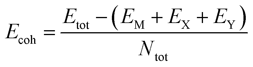 (EM, EX, EY, and EMXY are the total energies of a single M atom, a single X atom, a single Y atom and the MXY monolayer unit cell, respectively). Based on our computations, all formulated 2D Janus MXY monolayers exhibit robust energetic stability, with cohesive energies spanning from −3.46 eV per atom for MoBiI to −5.09 eV per atom for CrPF and CrPBr compounds. For clarity, the calculated relative cohesive energies for the designed 2D CrXY, MoXY, and WXY structures are depicted in Fig. 2(a)–(c). The figure presents the cohesive energy trends of 2D Janus CrXY, MoXY, and WXY monolayers, highlighting their relative thermodynamic stability. In all three cases, the cohesive energy increases (becomes less negative) as we move from phosphorus (P) to bismuth (Bi), indicating that lighter pnictogens contribute to greater stability. Among the halogen substitutions, fluorine-containing monolayers exhibit the most negative cohesive energies, implying the highest stability, followed by chlorine, bromine, and iodine, which aligns with the general trend of decreasing the bond strength for heavier halogens. These trends provide essential insights into the feasibility of experimental synthesis and the potential applications of these materials in opto-electronics and catalysis.
 | ||
| Fig. 2 The calculated cohesive energies of 2D Janus CrXY (a), MoXY (b), and WXY (c) structures. | ||
We then assessed the dynamic stability of the designed monolayers. To evaluate this, we analyzed their phonon spectra along the path connecting the highest symmetric points in their first Brillouin zone, Γ–M–K–Γ. The dymanic stability of the MXY monolayers are reported in Table 1. It is established that 12 out of 48 studied MXY monolayers are dynamically stable as there are no imaginary modes in the phonon dispersion curves of these structures. For instance, Fig. 1(c) and (e) show the positive phonon spectra of MoBiF and MoBiCl monolayers, which are dynamically stable. There are also 21 MXY monolayers with slightly negative phonon frequencies at the Γ-point, as shown in Fig. S1S3 (ESI†). These imaginary modes may arise from the limitations of the computational model, or the approximations used in the calculations, particularly those based on density functional theory (DFT).30–32 Moreover, they disappear when 2D structures are deposited on a suitable substrate because the substrate can effectively screen interactions that lead to negative phonon frequencies, thereby stabilizing the materials.30,33 Strain can also effectively stabilize the 2D materials by shifting the negative phonon frequencies into the positive regime.30–32,34 Therefore, such monolayers can also be considered as relatively stable materials. Fig. S1–S3 (ESI†) also depict the negative phonon frequencies of 15 MXY monolayers, indicating that these monolayers are not stable. The ZA, TA, and LA acoustic modes are crucial for heat conduction in narrow-gap semiconductors. ZA denotes the flexural acoustic mode, which is distinguished by atomic vibrations occurring in the z-direction. The terms LA and TA refer to the longitudinal and transverse acoustic modes, respectively. These modes involve atomic vibrations that occur within the plane of the 2D structures. Furthermore, upon examining the phonon spectra of the designed monolayers, it is evident that a significant phonon band gap is present in the spectra of MoXY and WXY monolayers. Specifically, this gap is observed in the following structures: MoPF, MoPCl, MoAsCl, MoSbCl, MoPBr, MoAsBr, MoSbBr, WPF, WPCl, WPBr, WAsF, WAsCl, and WAsBr (excluding the structures with the negative phonon frequency). A significant phonon band gap allows for the inhibition of optical phonon decay into acoustic phonons and reduces the rate at which carriers cool down.35 If there is no available path for optical phonons to convert into acoustic phonons, it is possible to sustain a population of hot optical phonons. Electrons have the ability to absorb optical phonons, which allows them to maintain a population of heated carriers. The presence of a gap in the phonon dispersion, specifically between the optical and acoustic branches, can eliminate the primary pathway for decay.36 Furthermore, to elucidate the bonding nature of these monolayers, the 2D electron densities of the MoSbBr and MoSbI structures are illustrated as a reference in Fig. 1(d) and (f). Upon closer examination of these figures, it becomes apparent that, within a specific transition metal-based compound, the energetic stability decreases as the size of the X element (the group V element) increases. Additionally, for a given combination of a transition metal and a halogen element, the energetic stability diminishes with an increase in the size of the X element (the group V element).
After assessing the stability of 2D Janus MXY monolayers, we investigated their electronic properties by calculating their band structures. To obtain more accurate band gaps, we employed the HSE06 functional. The band structures of 2D Janus MXY monolayers are depicted in Fig. S4–S6 of the ESI.† The band gaps EHSE06g (eV) of these monolayer materials are reported in Table 1. Our analysis reveals clear trends in the electronic properties of the monolayer systems composed of Cr, Mo, and W combined with group V elements (P, As, Sb, and Bi) and halogens (F, Cl, Br, and I). As the halogen is substituted from F to heavier elements like Cl, Br, and I, the band gap generally decreases, with several iodine-containing compounds exhibiting metallic behavior (zero band gap) compared to their semiconducting fluorine analogs. This trend is attributed to the increased lattice parameters and reduced orbital overlap associated with the larger, less electronegative halogens, which in turn lowers the energy separation between the conduction and valence bands.
Moreover, variations in the group V element further modulate the band gap, generally, with heavier elements tending to yield narrower gaps due to the increasing atomic size, which weakens the orbital overlap and reduces hybridization strength. However, deviations from this trend arise in several cases. For instance, CrBiF has a slightly higher band gap than CrSbF, likely due to weaker orbital hybridization and enhanced relativistic effects in Bi-containing systems, suggesting that subtle structural distortions and differences in bond lengths play a crucial role in shaping electronic behavior. Furthermore, the transition metal component also plays a significant role: Cr-based systems tend to have higher cohesive energies and wider band gaps, while Mo- and W-based compounds show more variable electronic behaviors under similar substitutions. These insights highlight the delicate interplay between atomic size, electronegativity, and orbital hybridization in tuning the electronic properties of two-dimensional materials, offering valuable guidance for the design of novel semiconductors and conductive materials.
For CrPI, MoPI, and WPI cases, by further assessment we realized that CrPI exhibits a half-metallic ferromagnetic nature, while MoPI and WPI show metallic behavior. Specifically, for the case of 2D CrPI, which exhibits a half-metallic electronic structure and a ferromagnetic ground state, the ferromagnetic ordering inherently breaks timereversal symmetry (TRS). Consequently, the system cannot support a Z2 topological classification, as Z2 (quantum spin hall state) invariants require preserved TRS. To assess the topological nature of the material, we calculated the Chern number. The Chern number serves as a topological invariant associated with the integral of Berry curvature over the entire Brillouin zone and is a hallmark of topologically nontrivial phases such as the quantum anomalous Hall effect (QAHE). A nonzero Chern number is indicative of a nontrivial topology, typically characterized by chiral edge states and quantized Hall conductance. However, the calculated Chern number for 2D CrPI is zero, signifying the absence of a net Berry curvature across the Brillouin zone. This result implies that the system does not exhibit any topological features associated with the QAHE or other topologically nontrivial phases. The zero Chern number indicates that Berry curvature contributions from the different regions of the Brillouin zone cancel out, leading to a topologically trivial phase. In summary, the ferromagnetic half-metallic nature of 2D CrPI, combined with its zero Chern number, confirms that the material is topologically trivial. Although its spin-polarized electronic structure and broken TRS are intriguing from a materials science perspective, they do not give rise to any topologically protected edge states or nontrivial topological order.
The observed band gap variations have significant implications for potential applications. Monolayers with moderate and tunable band gaps are promising for optoelectronics and photovoltaics, as they can absorb visible and near-infrared light efficiently. Meanwhile, metallic and narrow-gap systems are attractive for spintronics, where spin-polarized transport is crucial, and for catalytic applications, where metallic surfaces can facilitate redox reactions. The presence of an intrinsic built-in dipole due to the Janus structure enhances charge separation and could lead to improved performance in photocatalytic water splitting. The non-monotonic trends observed across different monolayers highlight the importance of external perturbations such as strain, doping, and applied electric fields in further modifying and optimizing their electronic properties. Strain engineering, in particular, could be a key tool for transforming indirect band gaps into direct ones, thereby enhancing their optoelectronic efficiency. These findings underscore the necessity for both theoretical and experimental investigations into the tunability of Janus monolayers, ensuring their integration into next-generation electronic, optical, and catalytic technologies.
When exploring potential applications of a material, the work function (Φ) is a crucial parameter in the analysis of electronic materials, along with the band structure; therefore, we calculated Φ using the equation Φ = Evac − EF, where Evac represents the vacuum level and EF denotes the Fermi level. These values were obtained from the electrostatic potential of the MoSbBr monolayer shown in Fig. 3(d). Due to the asymmetry in Janus materials, it is essential to consider the internal electric field resulting from the electronegativity difference between atomic layers. It is well-known that such intrinsic electric fields can enhance the separation of electron–hole pairs, beneficial for applications like photocatalytic water splitting.37 To account for this monolayer, dipole corrections were incorporated into the electrostatic potential calculations for vertically asymmetric Janus monolayers.38 Disrupting the vertical mirror symmetry in Janus structures leads to varying electrostatic potentials (ΔΦ) between the bottom (0 0 ![[1 with combining macron]](https://www.rsc.org/images/entities/char_0031_0304.gif) ) and top (0 0 1) surfaces, as illustrated in Fig. 3(d). This variation is reflected as differences in work functions on the opposite sides of the Janus materials. Table S1 in the ESI† details the ΔΦ values, indicating changes in electronegativity between layers.
) and top (0 0 1) surfaces, as illustrated in Fig. 3(d). This variation is reflected as differences in work functions on the opposite sides of the Janus materials. Table S1 in the ESI† details the ΔΦ values, indicating changes in electronegativity between layers.
 | ||
| Fig. 3 The band structures of 2D Janus MoSbBr (a), MoSbI (b) and WBiCl (c) monolayers, work function of MoSbBr (d), and (e) band alignments of 2D Janus MoSbBr, MoSbI and WBiCl monolayers. | ||
The moderate electrical band gap exhibited by these materials positions them as promising candidates for a variety of applications, including solar cells and water splitting. Furthermore, the inclusion of transition metals in these materials results in strong spin–orbit coupling, which could be harnessed for spin-valley optoelectronic applications. In this paper, we focus specifically on water splitting and the spin–orbit band splitting properties of these materials. The water splitting process involves two fundamental reactions: the hydrogen evolution reaction (HER) and the oxygen evolution reaction (OER); 2H+ + 2e− → H2, E0 = 0.00 eV and 2H2O → O2 + 4H+, E0 = 1.23 eV, concluding; H2O → 1/2O2 + 2H+, E0 = 1.23 eV. In the search for promising photocatalytic materials, the primary strategy revolves around finding materials with strong visible light absorption,39 leading to the generation of electron–hole pairs that can participate in the HER and OER reactions on the catalyst surface. To achieve this objective, certain criteria must be met:
• The material should be a semiconductor with a moderate bandgap, ideally greater than 1.23 eV.
• It should exhibit minimal recombination charge centers to ensure efficient separation and rapid transfer of photo-generated electrons and holes.
• The material's band edges must be appropriately positioned. Specifically, at pH = 0, the valence band minimum (VBM) should be lower than −5.67 eV, while the conduction band minimum (CBM) should be higher than −4.44 eV.
Considering the calculated moderate band gaps, by using Mulliken electronegativity rules,40–42 we computed the absolute positions of the VBM and CBM that would give us an initial insight into use in water splitting applications. Based on the Mulliken electronegativity rules that are EVBM = χ − EC + 1/2Eg and ECBM = χ − EC − 1/2Eg in which Eg is the band gap of the considered material, EC is the energy of the free electron in the hydrogen scale (4.5 eV), χ represents the Mulliken electro-negativity that can be obtained by  (a, b, …, z are the numbers of each atom in the compound) and EVBM and ECBM are the energies at the VBM and CBM, respectively, and
  (Eea and Ei refer to the electron affinity and the first ionization energy of the m element).
Utilizing the calculated band gaps, we determined the band edges for all compounds, as summarized in Table 1. Our analysis indicates that among the stable monolayer structures predicted, three structures including MoSbBr, MoSbI and WBiCl exhibit considerable potential for application in water splitting. The band edges of MoSbBr, MoSbI and WBiCl are presented in Fig. 3. It is worth noting that while the obtained band gaps and positions of the valence band maximum (VBM) and conduction band minimum (CBM) suggest promising applications of MoSbBr, MoSbI and WBiCl monolayers for water splitting, further analysis involving the calculation of the Gibbs free energy for the hydrogen evolution reaction (HER) and oxygen evolution reaction (OER) is essential for accurately assessing the photocatalytic water splitting potential. Moreover, considering the calculated band gaps and absolute band edge positions, a detailed study of strain effects on the electronic, optical and water splitting properties of these materials is suggested.41,43,44
The efficiency of solar energy conversion into hydrogen is a critical qualitative metric for solar energy water splitting photocatalysts. The calculated solar-to-hydrogen (STH) efficiency is high (see Discussion S1 for more information, ESI†). Table 2 lists the overpotentials for the hydrogen and oxygen evolution reactions χ (H2) and χ (O2), as well as the efficiency of light absorption (ηabs) and carrier utilisation (ηcu) for MoSbBr, MoSbI, and WBiCl monolayers (refer to the ESI†). The light absorption efficiency (ηabs) of the MoSbBr, MoSbI, and WBiCl monolayers exceeds 50% and is significantly dependent on the band gap value. Furthermore, the optimum levels of χ (H2) and χ (O2) result in energy conversion efficiencies of carrier utilization (ηcu) that exceed 35%. The high efficiencies of ηabs and ηcu result in a high STH efficiency (ηSTH). The ηSTH of these monolayers exceeds 10%, surpassing that of pentagonal PdSe2 (12.59%),45 GeN3 (12.63%),46 Janus WSSe (11.7%),47 β-Te2S and β-Te2Se (13.46% and 12.09%),48 Ge2Se2P4 (12.334%),49 and NbOX2 (X = Cl, Br, and I) monolayers (14.11–17.05%).50 As a result, we believe that the Janus MoSbBr, MoSbI, and WBiCl monolayers reach the essential value for affordable hydrogen production by photocatalysis (over 10%).
| E CBM | E CBM | χ (H2) | χ (O2) | η abs | η cu | η STH | |
|---|---|---|---|---|---|---|---|
| MoSbBr | −4.36 | −6.00 | 0.08 | 0.33 | 54.32 | 37.84 | 14.87 |
| MoSbI | −4.42 | −5.94 | 0.02 | 0.27 | 60.53 | 37.22 | 14.42 |
| WBiCl | −4.43 | −6.01 | 0.01 | 0.34 | 57.20 | 39.87 | 19.83 |
The 2D Janus MXY monolayer structures, similar to the 2D Janus TMDs (MXY), have a asymmetric structure with a C3v point group. This is in contrast to the single-layer MX2 TMD structure, which has a higher symmetry of the D3h point group.51,52 The asymmetrical configuration of the crystal structure of these Janus 2D materials creates a fundamental electric field, resulting in the separation of spin and valley states, as well as the Rashba effect when paired with spin–orbit coupling (SOC). In modern times, spin and valley are seen as additional degrees of freedom that are apart from the electronic charge. They offer a fascinating opportunity in the field of semiconductor devices.53,54 The combination of spin–orbit coupling (SOC) and a break of inversion symmetry in Janus TMDs leads to the occurrence of Zeeman-type spin splitting at the corners of the 2D Brillouin zone.
In order to study the spin valley splitting effect, we did an examination specifically focusing on the band structure of the 2D Janus CrAsCl monolayer. We used the PBE + SOC level of theory as a reference for our analysis. Significantly, it is noted that although the predicted band gap values may differ, all other band characteristics stay constant irrespective of the chosen functional. The utilization of the HSE06 approach results in an enlargement of the band gap, primarily due to the inclusion of the precise exchange interaction. Therefore, employing the PBE + SOC level of theory offers useful insights into the spin valley splitting in the suggested monolayers. Fig. 4(a) and (b) illustrate the band structure of the CrAsCl monolayer, which was determined using the PBE level of theory. The first figure shows the band structure without taking spin–orbit coupling (SOC) into account, while the second figure includes the effects of SOC. The image clearly demonstrates that the monolayer CrAsCl displays characteristics of a semiconductor with an indirect (quasi-direct) bandgap. The valence band maximum (VBM) and conduction band minimum (CBM) are located at the K/K′ point and somewhere along the K/K′–Γ route, respectively. When the SOC is included, Fig. 4(b) and (c) demonstrate that spin–orbit coupling mostly causes the separation of spins inside degenerate bands. This event occurs due to the violation of inversion symmetry, which causes the spin degeneracy to be disrupted at each generic k-point. Although time-reversal symmetry is maintained, the spin polarization at the K and K′ locations exhibit different orientations due to the time-reversal operation that links these sites. Furthermore, features that display anomalous behavior when subjected to the time-reversal operation will have contrasting characteristics at the K and K′ points. These data show the existence of a separate valley degree of freedom, therefore validating the long-desired valley polarization. In this context, valley polarization is represented as ΔV = EK′ − EK, where it represents the disparity in energy between the highest point of the valence band at K and K′ valleys. According to our calculations, activating the spin–orbit coupling (SOC) causes the spin degeneracy to be removed, resulting in a decrease in the band gap from 0.95 to 0.92 eV. Significantly, a valley spin splitting of 67 meV occurs near the valence band edge due to the pronounced influence of the strong spin–orbit coupling (SOC). The conduction band edges have a negligible valley spin splitting (10 meV) in comparison to the valence band. This is related to the dominance of distinct orbitals at the valence and conduction band edges.
 | ||
| Fig. 4 Band structure of the CrAsCl monolayer calculated by the PBE level of theory without spin–orbit coupling (a), band structure of the CrAsCl monolayer calculated by the PBE level of theory with spin–orbit coupling (b), schematic of valley selective excitation in which the red and blue colors denote the spin-up and spin-down states, respectively (c), and the schematic diagram of Rashba spin-splitting around the Γ point in the valence band (d). | ||
In addition, the disruption of mirror symmetry in Janus materials can induce Rashba spin splitting phenomena. This phenomenon arises from an internal electric field that is oriented perpendicular to the material. The electric field is created by the difference in electronegativity between the atomic layers of Janus structures, those are such materials that are based on transition metal dichalcogenides.55 We can see a significant Rashba splitting at the Γ point in the valence band of Janus MXY monolayers, as shown in Fig. 4(d). The intensity of the Rashba spin–orbit coupling splitting is determined by three parameters: the Rashba energy (ER), the momentum offset (KR), and the Rashba constant (αR). The values of ER and KR are obtained from the band structures,56–58 and the Rashba constant αR is calculated using the formula αR = 2ER/KR. The Rashba-type spin splitting at the Γ point is shown schematically in Fig. 4(d). Table 3 displays the calculated values of ΔV, ΔC, ER, KR, and αR for the 2D Janus MXY family. The splitting pattern follows the trend of increasing atomic weights, with SOC having a greater influence on elements like as W > Mo > Cr and Bi > Sb > As > P.
| Monolayer | ΔV | ΔC | E R | K R | α R |
|---|---|---|---|---|---|
| CrPF | 0.0559 | 0.0043 | 0.0026 | 0.0367 | 0.1417 |
| CrPCl | 0.059 | 0.004 | 0.0007 | 0.0208 | 0.0673 |
| CrPBr | 0.0737 | 0.0088 | 0.0005 | 0.0201 | 0.0498 |
| CrPI | — | — | — | — | — |
| CrAsF | 0.068 | 0.018 | 0.0065 | 0.0718 | 0.1811 |
| CrAsCl | 0.073 | 0.015 | 0.0055 | 0.0475 | 0.2316 |
| CrAsBr | 0.083 | 0.018 | 0.0027 | 0.0341 | 0.1584 |
| CrAsI | 0.093 | 0.019 | 0.0017 | 0.025 | 0.136 |
| CrSbF | — | — | — | — | — |
| CrSbCl | 0.0932 | 0.0257 | 0.0025 | 0.0716 | 0.0698 |
| CrSbBr | 0.0984 | 0.026 | 0.0022 | 0.0379 | 0.1161 |
| CrSbI | 0.1045 | 0.0232 | 0.0075 | 0.0544 | 0.2757 |
| CrBiF | — | — | — | — | — |
| CrBiCl | — | — | — | — | — |
| CrBiBr | — | — | — | — | — |
| CrBiI | 0.1446 | 0.0479 | 0.0109 | 0.0946 | 0.2304 |
| MoPF | 0.1005 | 0.0246 | 0.0015 | 0.021 | 0.1429 |
| MoPCl | 0.1134 | 0.0054 | 0.0007 | 0.0133 | 0.1053 |
| MoPBr | 0.136 | 0.0129 | 0.0009 | 0.0194 | 0.0928 |
| MoPI | — | — | — | — | — |
| MoAsF | 0.1162 | 0.0388 | 0.0282 | 0.0756 | 0.746 |
| MoAsCl | 0.1322 | 0.0193 | 0.0063 | 0.0327 | 0.3853 |
| MoAsBr | 0.1502 | 0.0251 | 0.0041 | 0.0255 | 0.3216 |
| MoAsI | 0.165 | 0.0302 | 0.0031 | 0.0246 | 0.252 |
| MoSbF | 0.1388 | 0.0359 | 0.0107 | 0.0792 | 0.2702 |
| MoSbCl | 0.1649 | 0.0332 | 0.011 | 0.0634 | 0.347 |
| MoSbBr | 0.1774 | 0.0355 | 0.0115 | 0.0496 | 0.4637 |
| MoSbI | 0.1897 | 0.0385 | 0.0164 | 0.0418 | 0.7847 |
| MoBiF | 0.1902 | 0.1541 | 0.0077 | 0.0511 | 0.3014 |
| MoBiCl | 0.2481 | 0.1204 | 0.0046 | 0.031 | 0.2968 |
| MoBiBr | 0.2524 | 0.1132 | 0.002 | 0.0121 | 0.3306 |
| MoBiI | 0.2535 | 0.0962 | 0.0149 | 0.041 | 0.7268 |
| WPF | 0.262 | 0.1011 | 0.0157 | 0.0631 | 0.4976 |
| WPCl | 0.2876 | 0.0049 | 0.005 | 0.04 | 0.25 |
| WPBr | 0.3069 | 0.0389 | 0.0081 | 0.04 | 0.405 |
| WPI | — | — | — | — | — |
| WAsF | 0.2837 | 0.0534 | 0.0578 | 0.1312 | 0.8811 |
| WAsCl | 0.3255 | 0.0383 | 0.0325 | 0.0788 | 0.8249 |
| WAsBr | 0.3463 | 0.0095 | 0.016 | 0.0571 | 0.5604 |
| WAsI | 0.3422 | 0.0059 | 0.0141 | 0.0607 | 0.4646 |
| WSbF | 0.3133 | 0.1746 | 0.0424 | 0.1529 | 0.5546 |
| WSbCl | 0.3788 | 0.084 | 0.0356 | 0.1267 | 0.562 |
| WSbBr | 0.3994 | 0.0563 | 0.042 | 0.1229 | 0.6835 |
| WSbI | 0.3958 | 0.0388 | 0.0339 | 0.0828 | 0.8188 |
| WBiF | 0.3701 | 0.005 | 0.0412 | 0.1353 | 0.609 |
| WBiCl | 0.4518 | 0.0113 | 0.0313 | 0.1234 | 0.5073 |
| WBiBr | 0.4643 | 0.0205 | 0.03 | 0.1265 | 0.4743 |
| WBiI | 0.4533 | 0.0295 | 0.0332 | 0.105 | 0.6324 |
The computed Rashba parameters αR are as follows: for CrXY, they range from 0.0498 to 0.2757 (eV Å); for MoXY, from 0.0928 to 0.7460 (eV Å); and for WXY, from 0.2500 to 0.8811 (eV Å). The αR value for 2D Janus MXY is comparable to those of (Mo and W)X2 (X = S and Se) (0.14–0.26 eV Å),59 traditional TMDs (0.05–0.40 eV Å),55 MoSSe (0.53 eV Å), WSSe (0.72 eV Å), WSeTe (0.92 eV Å),60 ZrS2Se (0.717 eV Å) and HfS2Se (0.566 eV Å),61 SnSTe (0.755 eV Å) and SnSeTe (0.273 eV Å),62 CrSTe (0.31 eV Å),63 and WSiAs3H (0.675 eV Å).57
4 Conclusion
First principles calculations based on density functional theory were performed to discover a diverse family of 48 2D Janus MoS2-like monolayers with the formula MXY. Many of these monolayers exhibit both energetic and dynamic stability, confirmed by their cohesive energy and phonon dispersion calculations. Most of the monolayers are semiconductors with moderate band gaps, making them promising for optoelectronic applications like solar cells and water splitting. The MoSbBr, MoSbI, and WBiCl monolayers show notable potential for water splitting due to their band structures. The inclusion of transition metals in the MXY monolayer is accompanied by a strong spin–orbit coupling effect, opening possibilities for spin-valley optoelectronics. The analysis of the electronic features reveals the quasi-direct band gap in some monolayers, which raises the necessity for a detailed band structure study. Spin-valley splitting was observed in CrAsCl monolayers. Rashba spin splitting occurs due to internal electric fields caused by the differing electronegativity of atomic layers. Rashba splitting near the Γ point in Janus MXY monolayers follows the trend W > Mo > Cr and Bi > Sb > As > P, with computed Rashba parameters ranging from 0.0498 to 0.8811 (eV Å), depending on the elements involved. Overall, this family of 2D Janus materials holds significant promise for future electronic, photonic, and catalytic technologies. Further experimental validation and research into the strain effects and catalytic performance will be essential for realizing their full potential.Data availability
The data that support the findings of this study are available from the corresponding author upon reasonable request.Conflicts of interest
There are no conflicts of interest to declare.Acknowledgements
This work was supported by the National Research Council of Canada through the Artificial Intelligence for Design program and Applied Quantum Computing (AQC) Program, and by the Natural Sciences and Engineering Research Council of Canada. The authors also acknowledge financial support from Defense Research and Development Canada (DRDC). C. E. E. acknowledges support from the U.S. National Science Foundation under Award No. DMR-2202101. The authors thank Dr. Tuan V. Vu and Dr. A. I. Kartamyshev (Van Lang University) for their valuable discussions during the development of this work.References
- K. S. Novoselov, A. K. Geim, S. V. Morozov, D.-E. Jiang, Y. Zhang, S. V. Dubonos, I. V. Grigorieva and A. A. Firsov, Science, 2004, 306, 666–669 Search PubMed.
- M. J. Allen, V. C. Tung and R. B. Kaner, Chem. Rev., 2010, 110, 132–145 Search PubMed.
- C. Soldano, A. Mahmood and E. Dujardin, Carbon, 2010, 48, 2127–2150 CrossRef CAS.
- B. Radisavljevic, A. Radenovic, J. Brivio, V. Giacometti and A. Kis, Nat. Nanotechnol., 2011, 6, 147–150 CrossRef CAS PubMed.
- Q. H. Wang, K. Kalantar-Zadeh, A. Kis, J. N. Coleman and M. S. Strano, Nat. Nanotechnol., 2012, 7, 699–712 CrossRef CAS PubMed.
- S. Z. Butler, S. M. Hollen, L. Cao, Y. Cui, J. A. Gupta, H. R. Gutiérrez, T. F. Heinz, S. S. Hong, J. Huang and A. F. Ismach, et al. , ACS Nano, 2013, 7, 2898–2926 CrossRef CAS PubMed.
- H. Liu, A. T. Neal, Z. Zhu, Z. Luo, X. Xu, D. Tománek and P. D. Ye, ACS Nano, 2014, 8, 4033–4041 Search PubMed.
- B. Anasori, M. R. Lukatskaya and Y. Gogotsi, MXenes, Jenny Stanford Publishing, 2023, pp. 677–722 Search PubMed.
- S. Manzeli, D. Ovchinnikov, D. Pasquier, O. V. Yazyev and A. Kis, Nat. Rev. Mater., 2017, 2, 1–15 Search PubMed.
- X. Liu, Q. Li, Q. Ruan, M. S. Rahn, B. I. Yakobson and M. C. Hersam, Nat. Mater., 2022, 21, 35–40 CrossRef CAS PubMed.
- M. Chhowalla, H. S. Shin, G. Eda, L.-J. Li, K. P. Loh and H. Zhang, Nat. Chem., 2013, 5, 263–275 CrossRef PubMed.
- J. A. Wilson, F. Di Salvo and S. Mahajan, Adv. Phys., 1975, 24, 117–201 CrossRef CAS.
- J. Xie, H. Zhang, S. Li, R. Wang, X. Sun, M. Zhou, J. Zhou, X. W. Lou and Y. Xie, Adv. Mater., 2013, 5807–5813 CrossRef CAS PubMed.
- Y. Shi, C. Hua, B. Li, X. Fang, C. Yao, Y. Zhang, Y.-S. Hu, Z. Wang, L. Chen and D. Zhao, et al. , Adv. Funct. Mater., 2013, 23, 1832–1838 CAS.
- O. Lehtinen, H.-P. Komsa, A. Pulkin, M. B. Whitwick, M.-W. Chen, T. Lehnert, M. J. Mohn, O. V. Yazyev, A. Kis and U. Kaiser, et al. , ACS Nano, 2015, 9, 3274–3283 CAS.
- L. Cheng, W. Huang, Q. Gong, C. Liu, Z. Liu, Y. Li and H. Dai, Angew. Chem., Int. Ed., 2014, 53, 7860–7863 CAS.
- D. Braga, I. Gutiérrez Lezama, H. Berger and A. F. Morpurgo, Nano Lett., 2012, 12, 5218–5223 CAS.
- W. Zhao, Z. Ghorannevis, L. Chu, M. Toh, C. Kloc, P.-H. Tan and G. Eda, ACS Nano, 2013, 7, 791–797 CrossRef CAS PubMed.
- J.-K. Huang, J. Pu, C.-L. Hsu, M.-H. Chiu, Z.-Y. Juang, Y.-H. Chang, W.-H. Chang, Y. Iwasa, T. Takenobu and L.-J. Li, ACS Nano, 2014, 8, 923–930 CrossRef CAS PubMed.
- A.-Y. Lu, H. Zhu, J. Xiao, C.-P. Chuu, Y. Han, M.-H. Chiu, C.-C. Cheng, C.-W. Yang, K.-H. Wei and Y. Yang, et al. , Nat. Nanotechnol., 2017, 12, 744–749 CrossRef CAS PubMed.
- J. Zhang, S. Jia, I. Kholmanov, L. Dong, D. Er, W. Chen, H. Guo, Z. Jin, V. B. Shenoy and L. Shi, et al. , ACS Nano, 2017, 11, 8192–8198 CrossRef CAS PubMed.
- L. Du, T. Hasan, A. Castellanos-Gomez, G.-B. Liu, Y. Yao, C. N. Lau and Z. Sun, Nat. Rev. Phys., 2021, 3, 193–206 CAS.
- G. Scuri, T. I. Andersen, Y. Zhou, D. S. Wild, J. Sung, R. J. Gelly, D. Bérubé, H. Heo, L. Shao and A. Y. Joe, et al. , Phys. Rev. Lett., 2020, 124, 217403 CrossRef CAS PubMed.
- G. Kresse and J. Furthmüller, Phys. Rev. B:Condens. Matter Mater. Phys., 1996, 54, 11169 CAS.
- G. Kresse and J. Furthmüller, Comput. Mater. Sci., 1996, 6, 15–50 CAS.
- P. E. Blöchl, Phys. Rev. B:Condens. Matter Mater. Phys., 1994, 50, 17953 Search PubMed.
- J. P. Perdew, K. Burke and M. Ernzerhof, Phys. Rev. Lett., 1996, 77, 3865 CrossRef CAS PubMed.
- A. Togo and I. Tanaka, Scr. Mater., 2015, 108, 1–5 CrossRef CAS.
- A. V. Krukau, O. A. Vydrov, A. F. Izmaylov and G. E. Scuseria, J. Chem. Phys., 2006, 125, 224106 CrossRef PubMed.
- W. Zhong and D. Vanderbilt, Phys. Rev. Lett., 1995, 74, 2587 CrossRef CAS PubMed.
- X.-P. Li and D. Vanderbilt, Phys. Rev. Lett., 1992, 69, 2543 CrossRef CAS PubMed.
- H. Zheng, X.-B. Li, N.-K. Chen, S.-Y. Xie, W. Q. Tian, Y. Chen, H. Xia, S. Zhang and H.-B. Sun, Phys. Rev. B:Condens. Matter Mater. Phys., 2015, 92, 115307 CrossRef.
- A. Furrer and W. Hälg, Phys. Status Solidi B, 1970, 42, 821–833 Search PubMed.
- R. Maiti, C. Patil, M. Saadi, T. Xie, J. Azadani, B. Uluutku, R. Amin, A. Briggs, M. Miscuglio and D. Van Thourhout, et al. , Nat. Photonics, 2020, 14, 578–584 Search PubMed.
- P. Blaha, K. Schwarz, G. Madsen, D. Kvasnicka, J. Luitz and K. Schwarz, An Augmented PlaneWave+ Local Orbitals Program for Calculating Crystal Properties, revised edition, WIEN2k 13.1 (Release 06/26/2013), Wien2K Users Guide, Isbn 3-9501031-1 9501031-2 technical report, 2008.
- G. Conibeer, D. König, M. Green and J. Guillemoles, Thin Solid Films, 2008, 516, 6948–6953 CrossRef CAS.
- Z. Cheng, Z. Hu, X. Ma, M. Wang, N. Gan and M. Pan, J. Phys. Chem. C, 2022, 126, 11510–11517 CrossRef CAS.
- L. Bengtsson, Phys. Rev. B:Condens. Matter Mater. Phys., 1999, 59, 12301 Search PubMed.
- Z. Cheng, Z. Hu, Z. Liu, C. Han, M. Wang, J. He, W. Zou and X. Ma, Surf. Interfaces, 2022, 31, 102082 CrossRef CAS.
- R. S. Mulliken, J. Chem. Phys., 1934, 2, 782–793 CrossRef CAS.
- M. Naseri, J. Phys. Chem. C, 2023, 127, 1687–1696 CrossRef CAS.
- D. D. Vo, T. V. Vu, A. Kartamyshev, T. H. Ho and N. N. Hieu, Nanoscale Adv., 2024, 6, 6019–6028 RSC.
- M. Naseri, D. R. Salahub, T. V. Vu and H. Zakaryae, J. Mater. Chem. C, 2022, 10, 11424 RSC.
- A. Bafekry, M. Naseri, M. Faraji, M. Fadlallah, D. Hoat, H. Jappor, M. Ghergherehchi, D. Gogova and H. Afarideh, Sci. Rep., 2022, 12, 22269 CrossRef CAS PubMed.
- C. Long, Y. Liang, H. Jin, B. Huang and Y. Dai, ACS Appl. Energy Mater., 2018, 2, 513–520 CrossRef.
- J. Liu, Y. Shen, X. Gao, L. Lv, Y. Ma, S. Wu, X. Wang and Z. Zhou, Appl. Catal., B, 2020, 279, 119368 CrossRef CAS.
- L. Ju, M. Bie, X. Tang, J. Shang and L. Kou, ACS Appl. Mater. Interfaces, 2020, 12, 29335–29343 CAS.
- J. Singh and A. Kumar, J. Mater. Chem. C, 2023, 11, 1173–1183 RSC.
- T. V. Vu, N. N. Hieu, D. D. Vo, A. Kartamyshev, H. D. Tong, T. T. Trinh, V. Khuong Dien, Z. Haman, P. Dey and N. Khossossi, J. Phys. Chem. C, 2024, 128, 4245–4257 CrossRef CAS.
- L. Pan, Y.-L. Wan, Z.-Q. Wang, H.-Y. Geng and X.-R. Chen, J. Appl. Phys., 2023, 134, 085105 CrossRef CAS.
- L. Dong, J. Lou and V. B. Shenoy, ACS Nano, 2017, 11, 8242–8248 CrossRef CAS PubMed.
- R. Li, Y. Cheng and W. Huang, Small, 2018, 14, 1802091 CrossRef PubMed.
- M. Abdollahi and M. B. Tagani, J. Mater. Chem. C, 2020, 8, 13286–13296 RSC.
- D. Xiao, G.-B. Liu, W. Feng, X. Xu and W. Yao, Phys. Rev. Lett., 2012, 108, 196802 CrossRef PubMed.
- T. Hu, F. Jia, G. Zhao, J. Wu, A. Stroppa and W. Ren, Phys. Rev. B, 2018, 97, 235404 CrossRef CAS.
- S. Singh and A. H. Romero, Phys. Rev. B, 2017, 95, 165444 CrossRef.
- T. V. Vu, B. D. Hoi, A. Kartamyshev and N. N. Hieu, J. Appl. Phys., 2024, 135, 074301 CrossRef CAS.
- T. V. Vu, N. P. Anh, H. V. Phuc, A. Kartamyshev and N. N. Hieu, New J. Chem., 2023, 47, 11660–11668 RSC.
- X. Li, S. Zhang, H. Huang, L. Hu, F. Liu and Q. Wang, Nano Lett., 2019, 19, 6005–6012 CrossRef CAS PubMed.
- J. Chen, K. Wu, W. Hu and J. Yang, J. Am. Chem. Soc., 2022, 144, 20035–20046 CrossRef CAS PubMed.
- R. Ahammed, N. Jena, A. Rawat, M. K. Mohanta, Dimple and A. De Sarkar, J. Phys. Chem. C, 2020, 124, 21250–21260 CrossRef CAS.
- B. D. Bhat, J. Phys.: Condens. Matter, 2023, 35, 435301 CrossRef CAS PubMed.
- S. Chen, Z. Zeng, B. Lv, S. Guo, X. Chen and H. Geng, Phys. Rev. B, 2022, 106, 115307 CrossRef CAS.
Footnote |
| † Electronic supplementary information (ESI) available. See DOI: https://doi.org/10.1039/d4cp04036h |
| This journal is © the Owner Societies 2025 |