
Quantum spin Hall states in MX2 (M = Ru, Os; X = As, Sb) monolayers†
Tao
Jing
 *a,
Dongmei
Liang
a,
Yongchen
Xiong
a,
Jun
Zhang
a,
Yongjin
Hu
a,
Qin
Zhang
a,
Dongyan
Lv
a,
Zhi
He
a and
Mingsen
Deng
*b
*a,
Dongmei
Liang
a,
Yongchen
Xiong
a,
Jun
Zhang
a,
Yongjin
Hu
a,
Qin
Zhang
a,
Dongyan
Lv
a,
Zhi
He
a and
Mingsen
Deng
*b
aSchool of Mathematics, Physics and Optoelectronic Engineering, and Collaborative Innovation Center for Optoelectronic Technology, Hubei University of Automotive Technology, Shiyan 442002, People's Republic of China. E-mail: jingt87@sina.com
bGuizhou Provincial Key Laboratory of Computing and Network Convergence, School of Information, Guizhou University of Finance and Economics, Guiyang 550025, People's Republic of China. E-mail: deng@gznc.edu.cn
First published on 22nd November 2024
Abstract
The quantum spin Hall (QSH) effect has attracted extensive research interest due to its great promise in topological quantum computing and novel low-energy electronic devices. Here, using first-principles calculations, we find that MX2 (M = Ru and Os; X = As and Sb) monolayers are 2D topological insulators (TIs). The spin–orbit coupling (SOC) band gaps for RuAs2, RuSb2, OsAs2, and OsSb2 monolayers are predicted to be 80, 131, 118, and 221 meV, respectively. Additionally, the nontrivial topological states are further confirmed by calculating the topological invariant and the appearance of gapless edge states. More interestingly, for RuSb2 and OsSb2 monolayers, the position of node points in energy can be effectively tuned by applying in-plane strain. Our results consistently indicate that all MX2 monolayers can serve as an effective platform for achieving the room-temperature QSH effect.
1 Introduction
The band structure topology of insulating and semimetallic materials has garnered considerable attention in condensed matter physics and materials science.1–4 The unique topological features, such as conductive channels on surfaces or edges protected by various symmetries, hold great promise for applications in topological quantum computing and innovative low-energy electronic devices.5–7 By combining both an insulating bulk and a metallic surface, topological insulators (TIs) with quantum spin Hall (QSH) states have received special attention.8–10 With the protection of time-reversal symmetry, these states are marked by an odd number of surface-state bands and non-zero topological invariants. Besides, the robust conductive surface states of TIs are closely linked to band inversions and remain resilient to scattering by nonmagnetic impurities.11–13Graphene was the first system to be proposed as a QSH insulator via the spin-orbital coupling (SOC) effect.14 Unfortunately, the SOC effect of graphene is too weak, resulting in a too small bulk band gap on the order of 10−3 meV.15 Two dimensional (2D) HgTe/CdTe quantum wells were predicted and subsequently experimentally verified to realize the QSH effect.16,17 On the other hand, three-dimensional (3D) topological insulators, including Bi2Se3, Bi2Te3, and Sb2Te3, were discovered, sparking great research enthusiasm due to their unique electronic properties and ease of experimental synthesis.18 Numerous novel physical phenomena, including the QSH effect and the quantum anomalous Hall (QAH) effect, have been observed in this material system. For instance, the QAH effect has been realized in Cr-doped (Bi; Sb)2Te3 and V-doped (Bi; Sb)2Te3 films.19,20
2D TIs have demonstrated a fundamental interplay between the electronic structure and topology, offering a promising platform for applications in spintronics.21–30 There is great interest in the discovery of new 2D TIs, as this provides more options for experiments and applications.31,32 Consequently, intensive efforts have been devoted to the search for 2D materials with novel topological properties and a large amount of 2D TIs have been proposed theoretically.33–37 However, these topological materials proposed in theoretical works have rarely been confirmed experimentally. The low temperature required for QSHs, which arises from the small bulk gap, limits the practical applications of 2D TIs. Therefore, searching and designing 2D TIs with large energy gaps is essential to overcome thermal fluctuations and thus advance the realistic applications of QSH insulators.
Transition-metal dichalcogenides (TMDCs) have been studied intensively in recent years due to their diverse electronic and magnetic properties.38–40 For instance, the 1T′ structures of TMDC monolayers have been confirmed as quantum spin Hall (QSH) insulators.41 Following this discovery, other phases of TMDCs have also been predicted to exhibit the QSH state with large nontrivial gaps.42,43 On the other hand, transition metal dipnictides (TMDPs) have also been found to exhibit nontrivial topological properties. For example, single crystals of NbAs2 and TaAs2 have been synthesized and identified as potential candidates for topological semimetals (TSMs).44 Additionally, WP2 and MoP2 have been recognized as type-II Weyl semimetals with exceptionally high conductivity.45 However, much less attention has been paid to 2D TMDPs, especially with respect to their topological properties.
In this study, based on first-principles calculations, we investigated the electronic and topological properties of MX2 (M = Ru and Os; X = As and Sb) monolayers. These monolayers are confirmed to be dynamically and thermally stable by the phonon spectrum calculations and ab initio molecular dynamics (MD) simulations. The nontrivial band inversion occurs around the Γ point even when the SOC effect is neglected. These MX2 monolayers become topological insulators because the band gap opens upon the inclusion of the SOC effect. The calculated topological invariant and the appearance of gapless edge states indicate that these MX2 monolayers are promising candidates for realizing the QSH effect. More interestingly, for RuAs2 and OsSb2 monolayers, appropriate uniaxial tension strain can be applied to tune the position of node points in energy and further enlarge their nontrivial gaps.
2 Computational methods
Our calculations are carried out using the projector augmented wave (PAW) method within density functional theory (DFT) as implemented in the Vienna ab initio simulation package (VASP).46,47 Perdew–Burke–Ernzerhof (PBE) of generalized gradient approximation (GGA) is adopted for the exchange–correlation potential.48 The cutoff energy of the plane-wave basis is set to 500 eV, and the convergence threshold of total energy is set to 10−6 eV. The atomic positions and lattice parameters are optimized until the forces are smaller than 0.001 eV Å−1. A 20 Å thick vacuum layer is used to avoid interactions between the nearest slabs. The Brillouin zone is sampled with a 19 × 9 × 1 centered k point grid for geometry optimization and the computations on electronic properties,49 which guarantees the convergency of topological properties. As the PBE functional underestimates the bulk band gaps of TIs, the HSE06 method is also adopted for attaining an accurate result.50 The phonon spectra are calculated using the density functional perturbation theory implemented in the PHONOPY package.51 A 4 × 2 × 1 supercell is used for ab initio molecular dynamics (AIMD) simulations in the NVT ensemble at 300 K and 500 K for 5 ps.52 The tight-binding models are developed with the help of the WANNIER90 code on the basis of density functional theory (DFT) calculations.533 Results and discussion
All possible 2D planar structures of MX2 (M = Ru and Os; X = As and Sb) are searched by the particle swarm optimization (PSO) structure search method.54,55 We focus our structure search on MX2 monolayers with fixed atomic stoichiometry for M and X atoms (1![[thin space (1/6-em)]](https://www.rsc.org/images/entities/char_2009.gif) :2). The population size and the number of generations are set to be 40 and 30, respectively.56 Simulating cells containing two formula units are considered for MX2 monolayers. Here, the most energetically stable monolayers are taken into account for further calculations, which belong to the monoclinic system with a space group of P21/M (1T′ phase). Without a loss of generality, we take the RuAs2 monolayer as an example. The structure of the RuAs2 monolayer can be viewed as an As bilayer intercalated by a Ru layer, forming the edge-shared RuAs6 octahedron. The primitive unit cell contains two formula units of RuAs2, as shown in Fig. 1a. The corresponding lattice parameters of optimized structures are listed in Table S1 (ESI†). It is indicated that the lattice parameters increase as the composition elements change from As to Sb and from Ru to Os. The equilibrium lattice constants are found to be a = 3.062 Å and b = 6.360 Å, a = 3.273 Å and b = 6.648 Å, a = 3.093 Å and b = 6.358 Å, and a = 3.285 Å and b = 6.635 Å for RuAs2, RuSb2, OsAs2, and OsSb2 monolayers, respectively.
:2). The population size and the number of generations are set to be 40 and 30, respectively.56 Simulating cells containing two formula units are considered for MX2 monolayers. Here, the most energetically stable monolayers are taken into account for further calculations, which belong to the monoclinic system with a space group of P21/M (1T′ phase). Without a loss of generality, we take the RuAs2 monolayer as an example. The structure of the RuAs2 monolayer can be viewed as an As bilayer intercalated by a Ru layer, forming the edge-shared RuAs6 octahedron. The primitive unit cell contains two formula units of RuAs2, as shown in Fig. 1a. The corresponding lattice parameters of optimized structures are listed in Table S1 (ESI†). It is indicated that the lattice parameters increase as the composition elements change from As to Sb and from Ru to Os. The equilibrium lattice constants are found to be a = 3.062 Å and b = 6.360 Å, a = 3.273 Å and b = 6.648 Å, a = 3.093 Å and b = 6.358 Å, and a = 3.285 Å and b = 6.635 Å for RuAs2, RuSb2, OsAs2, and OsSb2 monolayers, respectively.
 | ||
| Fig. 1 (a) Top and side views of the crystal structure and (b) 2D Brillouin zone with specific symmetry points for the RuAs2 monolayer in the 1T′ phase. Top and side views of crystal structures for the RuSb2 monolayer in the (c) 2H and (d) 1T phase. | ||
Cohesive energy can be employed to access the energetic stability and experimental feasibility of predicted 2D materials.57 Here, the cohesive energy of the MX2 monolayer is calculated according to this expression:
| EC = EMX2 − EM − 2EX |
With this conception, we then identify the cohesive energies of these four predicted MX2 monolayers. As shown in Table S2 (ESI†), the resultant cohesive energies are −6.17, −5.70, −6.69, and −6.16 eV per atom for RuAs2, RuSb2, OsAs2, and OsSb2 monolayers, respectively, indicating high energetic stability. Thus, the high synthetic possibilities of the MX2 monolayers are expected to enhance their practical applications. As a comparison, the crystal structures of 1T and 2H phases are shown in Fig. 1c and d. In addition, the cohesive energies of 1T and 2H MX2 monolayers are also calculated and given in Table S2 (ESI†). We find that the cohesive energies of the 2H phases are slightly higher than those of 1T′ phases for all MX2 monolayers. However, the 1T phases are significantly unstable compared to the 1T′ and 2H phases, indicating the low synthetic possibility.
Next, we examine the dynamic stability of MX2 monolayers, and calculate the phonon spectra along the high-symmetry lines using the DFPT method, as plotted in Fig. 2a and Fig. S1 (ESI†). The absence of any appreciable imaginary frequency is found in the full Brillouin zone, confirming the dynamic stability of these MX2 monolayers. To validate their thermal stability, we performed AIMD simulations at 300 K and 500 K that lasted for 5 ps with a time step of 1 fs. Taking the RuAs2 monolayer as an example, the calculated results are shown in Fig. 2b and c. Although As atoms exhibit small deviations from their original sites due to thermal perturbations, neither bond breakage nor structure reconstruction is observed. Besides, it is also noted that the total energy fluctuation of the RuAs2 monolayer is considerably small at this temperature, as indicated in Fig. 2d and e. As shown in Table S3 (ESI†), the energy oscillation intervals for the MX2 monolayers are in the range of 0.47 to 0.57 eV at a heating temperature of 300 K. When the heating temperature reaches 500 K, the energy oscillation intervals significantly increase with values ranging from 0.70 to 0.91 eV. Next, we calculated the phonon spectrum of MX2 monolayers after heating at 300 K and 500 K for 5 ps, as indicated in Fig. S2 (ESI†). For RuAs2, RuSb2, and OsAs2 monolayers, a few imaginary frequencies appear near the Gamma point in acoustic branches when the heating temperature is 300 K. However, the OsSb2 monolayer shows some imaginary frequencies in the optical branches, indicating its weaker thermal stability. At a heating temperature of 500 K, RuAs2 and OsAs2 monolayers still exhibit only a small number of imaginary frequencies in the acoustic branches, indicating their high thermal and dynamic stability.
 | ||
| Fig. 2 (a) Phonon dispersion of the RuAs2 monolayer, indicating the dynamical stability of this monolayer. The structures of RuAs2 after 5 ps of AIMD simulation at (b) 300 K and (c) 500 K. Total potential energy fluctuations of AIMD simulation at (d) 300 K and (e) 500 K. | ||
To demonstrate the mechanical stability of MX2 monolayers, the elastic properties are investigated, as shown in Table 1. Taking the RuAs2 monolayer as an example, the calculated values of C11, C22, C12, and C44 are 79.77 N m−1, 79.72 N m−1, 21.90 N m−1, and 25.90 N m−1, respectively. Notably, the elastic constants for the RuAs2 monolayer satisfy the Born criteria of mechanical stability: C11C22 > C122 and C11, C22, C44 > 0, confirming its mechanical stability. The 2D Young's moduli C2D, shear modulus G2D, and Poisson's ratios ν2D for RuAs2 are calculated to be 73.75 N m−1, 28.93 N m−1, and 0.27, respectively. It is worth noting that the in-plane Young's moduli of RuAs2 are less than those of hexagonal h-BN (271 N m−1) and graphene (340 N m−1),58,59 indicative of good mechanical flexibility.
| Systems | Y 2Ds | G | ν | σ | h/l |
|---|---|---|---|---|---|
| RuAs2 | 73.69 | 28.93 | 0.27 | 1.849 × 10⁻⁶ | 2.906 × 10⁻⁴ |
| RuSb2 | 65.81 | 22.49 | 0.26 | 2.656 × 10⁻⁶ | 3.407 × 10⁻⁴ |
| OsAs2 | 91.29 | 35.37 | 0.26 | 2.896 × 10⁻⁶ | 3.144 × 10⁻⁴ |
| OsSb2 | 68.93 | 29.53 | 0.23 | 3.335 × 10⁻⁶ | 3.619 × 10⁻⁴ |
For these MX2 monolayers, we estimate the typical plane deformation caused by gravity using the following formula:

A detailed symmetry analysis is needed before the investigation of electronic structures for MX2 monolayers. It is known that the symmetry of MX2 monolayers belongs to space group 11, which contains the inversion symmetry P: (x, y, z) → (−x, −y, −z), and rotation symmetries C2x: (x, y, z) → (x + 1/2, −y, −z). Combining the two symmetry operations leads to the glide plane M2x: (x, y, z) → (−x + 1/2, y, z). Notably, time reversal symmetry T is preserved because these systems are non-magnetic. Without including the SOC, we obtain T2 = 1 and C2x2 = eikxa. The antunitary operator TC2x with the product (TC2x)2 = −1 is considered along the X–M line (kx, π, 0), leading to double degeneracy bands along this direction. With the presence of SOC, the bands are Kramers degenerate for all k due to the simultaneous satisfaction of P and T symmetries. Additionally, at the X (π, 0, 0) and M (π, π. 0) points, the C2x eigenvalues are ±1. Simultaneously, P and C2x satisfy the anticommutation relation {P, C2x} = −1. Therefore, the fourfold degeneracy bands are located in the X and M points even in the presence of SOC.
Then, we move to study the electronic properties of MX2 monolayers. The band structures are first calculated without considering SOC, as shown in Fig. 3a and Fig. S3 (ESI†). In addition, no spin polarization can be found for the band structures of MX2 monolayers, indicating that these systems are nonmagnetic. Further test calculations have been conducted using the GGA+U method with U values ranging from 1 to 3 eV for the Ru and Os d electrons to correct for Coulomb interactions. The calculated results indicate that no magnetic moment is present in the Ru and Os atoms. Interestingly, the 1T′ phase MX2 monolayers are gapless semiconductors, or alternatively semimetals. Obviously, the absence of a linear dispersion relation between the conduction and valence bands can be observed near the Fermi level. Thus, the band crossing points of these MX2 monolayers are classified as type-II Dirac points due to the breakdown of Lorentz symmetry.62–64 Notably, the conduction and valence bands of MX2 monolayers are inverted around the Γ point and cross each other along the Γ–X line when SOC is ignored, suggesting the nontrivial band topology. In addition, an electron pocket can be observed around the Y point. By analyzing the orbital components of the states near the Γ point, we note that the bands near the Fermi level mainly originate from 4 d orbitals of Ru atoms and 4 p orbitals of As atoms, as shown in Fig. 3b. A careful analysis of these states near the Γ point is needed to further explore its topological properties. As indicated in Fig. 3c, the calculated fat-band structures show that these states above the Fermi level are mainly contributed by pz orbitals of As atoms. While these states that are lower than the Fermi level are composed of dz2 orbitals of Ru atoms. Due to band inversion, the band crossing along the Γ–X line corresponds to accidental degeneracy. Notably, the band crossing in energy is about 0.05 eV above the Fermi level while the other bands are gapped. In addition, the band structures of RuSb2, OsAs2, and OsSb2 monolayers share similar features to those of RuAs2. After a careful symmetry analysis, we find that these crossing points are isolated rather than part of a nodal line, due to the absence of mirror symmetry protection. This accidental band touching near the Fermi energy can be attributed to the opposite parity of the two inverted bands. It is worth noting that the band inversion around the Γ point is not caused by SOC, as this interaction is absent. As shown in Fig. 3d, the 3D band structure confirms the presence of nodal points rather than a nodal line in the band structure near the Fermi level. To reveal the bonding characteristics of predicted 2D materials, the electron localization function (ELF) is calculated. The ELF is defined as:

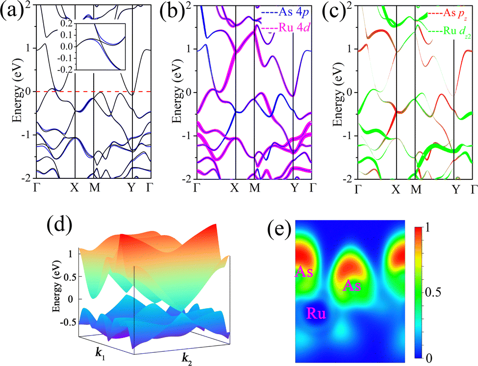 | ||
| Fig. 3 (a) Band structures of the RuAs2 monolayer without SOC and with SOC. The inset shows the gap opening in the presence of SOC. (b) and (c) Orbitally resolved band structure of the RuAs2 monolayer without SOC. (d) 3D representation of the band structure around the crossing point. The Fermi level is set as the zero reference. (e) Electron localization function (ELF) map of the RuAs2 monolayer. All results are calculated using the PBE functional. | ||
It will be important and interesting to further investigate the potential topological properties of proposed MX2 monolayers. Taking the SOC into account, the twofold degenerate bands can be observed at any k-vector of the Brillouin zone due to the presence of both P and T symmetries. Interestingly, the nodal points are gaped in the Γ–X line, as shown in Fig. 3a. In other words, a phase transition from gapless semimetal to an insulator can be realized. According to previous reports, the SOC-induced bandgap opening near the Fermi level indicates the nontrivial topological properties of these systems. It is also worth noting the lack of well-defined band gaps near the original crossing points when SOC is applied, as the indirect band is zero or negative. The hybrid functional calculation (HSE06) is employed to overcome the possible overestimation of band inversion in the PBE functional. Interestingly, we find that the band inversion remains, but the conduction band at the Y point is pushed above the Fermi level, resulting in the disappearance of the electron pocket observed in the PBE functional calculations, as illustrated in Fig. 4a. The calculated results indicate that the band inversions still occur using the HSE06 functional. The SOC band gap of the RuAs2 monolayer is about 80 meV, which can be seen from the inset of Fig. 4b. As sketched in Fig. S4 (ESI†), the opened gaps for RuSb2, OsAs2, and OsSb2 monolayers are as large as 131, 118, and 221 meV, respectively. Such large bandgaps imply that these monolayers are expected to realize the QSH effect at room temperature. In order to explore the nontrivial topological properties of RuAs2, the Z2 invariant is calculated by using the maximally localized Wannier functions. The evolution of the Wannier center of charges (WCCs) is adopted for the Z2 calculations. We calculate the Z2 number by counting the crossing number for any arbitrary horizontal reference line, as illustrated in Fig. 4c. As expected, an odd number of times in the kz = 0 plane can be found for the crossing between any arbitrary horizontal reference line and evolution lines of Wannier centers, yielding Z2 = 1. Similar to the RuAs2 monolayer, a gap opening at the original gapless crossing points can be observed for RuSb2, OsAs2, and OsSb2 monolayers, indicating the existence of the nontrivial topological phase, as shown in Fig. S4 (ESI†). The presence of topologically protected conducting edge states with a single Dirac cone at the Γ point can be observed, which connect the bulk valence and conduction bands, as displayed in Fig. 4d and Fig. S5 (ESI†).
 | ||
| Fig. 4 Band structures of RuAs2 (a) without SOC and (b) with SOC, with the Fermi level as the zero reference. (c) Evolution of the Wannier charge center (WCC) for RuAs2 along k. (d) Topological edge states of the semi-infinite RuAs2 nanoribbon with SOC. All results are calculated by the hybrid functional (HSE06) method. | ||
For the band structures of RuSb2 and OsSb2 monolayers, the crossing point in the X–Γ–X path remains above the Fermi level even in HSE06 calculations. In addition, some states of the conduction band cross the Fermi level, which may prevent the experimental observation of topological properties. As an effective way to tune the electronic properties of 2D materials, strain can be readily exerted by various strategies, such as lattice mismatch, bending, and application of stress on materials.66 We believe that strain has a significant impact on the electronic structures of MX2 monolayers. Therefore, the uniaxial strain is imposed on the planes of these systems by varying the planar lattice parameters. The strain magnitude is defined as ε = Δc/c, in which c and c + Δc represent the lattice constants of the unstrained and strained supercells, respectively. For RuSb2 and OsSb2 monolayers, the energy variations of the node points as a function of strain are calculated and given in Fig. 5, Fig. S6 and S7 (ESI†). Upon increasing the compressive strain from −1% to −5% in the x direction, the node point in energy shifts upward with its value varying from 0.24 to 0.40 eV for RuSb2. Instead, the energy of the node point varies from 0.14 to 0.03 eV upon increasing the tension strain. We can also observe a similar trend in the node point shift when the strain is applied in the y direction. Interestingly, these states around the node point become occupied under 5% tension strain. For the OsSb2 monolayer, the energy of the crossing point first increases and then decreases by increasing compressive strain in the x direction. For the OsSb2 monolayer, the Os–Sb bond length decreases with increasing compressive strain. As a result, the hybridization between the Os 5d and Sb 5p orbitals is enhanced, leading to the separation of valence and conduction bands. As indicated by the topological phase diagram in Fig. 5c and d,39 the node points disappear, and the topological phase transitions from nontrivial to trivial when the compressive strain in the x direction reaches −4% and in the y direction reaches −5%. The energy of the node point downshifts to 0.03 eV when the lattice constant of the OsSb2 monolayer in the x direction is stretched by 5%. This value reaches 0.02 eV when the 5% tension strain is applied in the y direction.
 | ||
| Fig. 5 The energies of node points as a function of strain for (a) RuSb2 and (b) OsSb2 monolayers, with the Fermi level as the zero reference. Topological phase diagram of the OsSb2 monolayer as a function of uniaxial strain along the (c) x and (d) y directions. All results are calculated using the PBE functional without including SOC. | ||
As discussed above, applying tensile strain pushes up the conduction band around the Y point, bringing the nodal points closer to the Fermi level in both RuSb2 and OsSb2 monolayers. Taking the OsSb2 monolayer as an example, we find that the energy gap at the Γ point becomes larger with a value of 236 eV at the HSE06 level, demonstrating the high possibility of observing QSH states at room temperature, as shown in Fig. 6a and b. In addition, the nontrivial band topologies can survive in a wide range of strain, which can be confirmed by topological invariants Z2. Finally, the edge states of the OsSb2 monolayer with 5% tension strain are studied. Fig. 6c summarizes the topological edge states of the semi-infinite OsSb2 nanoribbon with SOC under 5% tension strain. It is noted that these edge states, protected by time reversal symmetry, locate at the Γ point, revealing a nontrivial topology of these states.
 | ||
| Fig. 6 The band structure of the OsSb2 monolayer (a) with and (b) without SOC under 5% tension strain. (c) Topological edge states of the semi-infinite OsSb2 nanoribbon with SOC under 5% tension strain. | ||
4 Conclusions
In summary, based on first-principles calculation, we have proposed a new family of QSH insulators. Our results demonstrate that MX2 (M = Ru and Os; X = As and Sb) monolayers exhibit appreciable energetic, thermal, and dynamic stabilities. These monolayers exhibit TI characteristics and large SOC band gaps with values of 80, 131, 118, and 221 meV for RuAs2, RuSb2, OsSb2, and OsSb2, respectively. In addition, the strain can effectively tailor the electronic structures and topological properties of these MX2 monolayers. In detail, for the RuSb2 and OsSb2 monolayers, the node point in energies shifts downward toward the Fermi level under the tension strain. Our results consistently indicate that the proposed MX2 monolayers can provide an ideal platform for realizing the QSH effect at room temperature.Data availability
The data used to support the findings of this study are included within the article.Conflicts of interest
There are no conflicts to declare.Acknowledgements
This work is supported by the open fund of Hubei Key Laboratory of Energy Storage and Power Battery (HUAT) (grant No. ZDK22023A04), Shiyan Key Laboratory of Quantum Information and Precision Optics (Grant No. SYZDK12024B02), Doctoral Scientific Research Foundation of Hubei University of Automotive Technology (Grants No. BK202431 and Grant No. BK202429), and Guizhou Provincial Major Scientific and Technological Program (QKHZDZXZ[2024]022).References
- A. Bansil, H. Lin and T. Das, Colloquium: Topological band theory, Rev. Mod. Phys., 2016, 88, 021004 CrossRef.
- B. Q. Lv, T. Qian and H. Ding, Experimental perspective on three-dimensional topological semimetals, Rev. Mod. Phys., 2021, 93, 025002 CrossRef CAS.
- B. A. Bernevig, C. Felser and H. Beidenkopf, Progress and prospects in magnetic topological materials, Nature, 2022, 603, 41–51 CrossRef CAS PubMed.
- B. Yuan, W. Sun, Y. Bai, Z. Chen, B. Huang, Y. Dai and C. Niu, A mixed Weyl semimetal in a two-dimensional ferromagnetic BaCrSe2 monolayer, J. Mater. Chem. C, 2024, 12, 296–300 RSC.
- P. Liu, J. R. Williams and J. J. Cha, Topological nanomaterials, Nat. Rev. Mater., 2019, 4, 479–496 CrossRef CAS.
- F. Tang, H. C. Po, A. Vishwanath and X. Wan, Comprehensive search for topological materials using symmetry indicators, Nature, 2019, 566, 486–489 CrossRef CAS.
- G. Zhang, H. Wu, L. Zhang, L. Yang, Y. Xie, F. Guo, H. Li, B. Tao, W. Guo, W. Zhang and H. Chang, Two-Dimensional van der Waals Topological Materials: Preparation, Properties, and Device Applications, Small, 2022, 18, 2204380 CrossRef CAS.
- A. Roth, C. Brüne, H. Buhmann, L. W. Molenkamp, J. Maciejko, X. L. Qi and S. C. Zhang, Nonlocal transport in the quantum spin Hall state, Science, 2009, 325, 294–297 CrossRef CAS.
- M. Z. Hasan and C. L. Kane, Colloquium: topological insulators, Rev. Mod. Phys., 2010, 82, 3045–3067 CrossRef CAS.
- X. L. Qi and S. C. Zhang, Topological insulators and superconductors, Rev. Mod. Phys., 2011, 83, 1057–1110 CrossRef CAS.
- F. Zhang, C. L. Kane and E. J. Mele, Surface states of topological insulators, Phys. Rev. B:Condens. Matter Mater. Phys., 2012, 86, 081303 CrossRef.
- Q. Liu, X. Zhang, L. B. Abdalla, A. Fazzio and A. Zunger, Switching a normal insulator into a topological insulator via electric field with application to phosphorene, Nano Lett., 2015, 15, 1222–1228 CrossRef CAS.
- F. C. Chuang, L. Z. Yao, Z. Q. Huang, Y. T. Liu, C. H. Hsu, T. Das, H. Lin and A. Bansil, Prediction of large-gap two-dimensional topological insulators consisting of bilayers of group III elements with Bi, Nano Lett., 2014, 14, 2505–2508 CrossRef CAS.
- C. L. Kane and E. J. Mele, Z2 topological order and the quantum spin Hall effect, Phys. Rev. Lett., 2005, 95, 146802 CrossRef CAS.
- Z. Qiao, S. A. Yang, W. Feng, W. K. Tse, J. Ding, Y. Yao, J. Wang and Q. Niu, Quantum anomalous Hall effect in graphene from Rashba and exchange effects, Phys. Rev. B:Condens. Matter Mater. Phys., 2010, 82, 161414 CrossRef.
- B. A. Bernevig, T. L. Hughes and S. C. Zhang, Quantum spin Hall effect and topological phase transition in HgTe quantum wells, Science, 2006, 314, 1757–1761 CrossRef CAS.
- M. Konig, S. Wiedmann, C. Brune, A. Roth, H. Buhmann, L. W. Molenkamp, X. L. Qi and S. C. Zhang, Quantum spin Hall insulator state in HgTe quantum wells, Science, 2007, 318, 766–770 CrossRef.
- H. Zhang, C. X. Liu, X. L. Qi, X. Dai, Z. Fang and S. C. Zhang, Topological insulators in Bi2Se3, Bi2Te3 and Sb2Te3 with a single Dirac cone on the surface, Nat. Phys., 2009, 5, 438–442 Search PubMed.
- C. Z. Chang, J. Zhang, X. Feng, J. Shen, Z. Zhang, M. Guo, K. Li, Y. Ou, P. Wei, L.-L. Wang, Z. Q. Ji, Y. Feng, S. Ji, X. Chen, J. Jia, X. Dai, Z. Fang, S. C. Zhang, K. He, Y. Wang, L. Lu, X. C. Ma and Q. K. Xue, Experimental observation of the quantum anomalous Hall effect in a magnetic topological insulator, Science, 2013, 340, 167–170 CrossRef CAS.
- C. Z. Chang, W. Zhao, D. Y. Kim, H. Zhang, B. A. Assaf, D. Heiman, S. C. Zhang, C. Liu, M. H. W. Chan and J. S. Moodera, High-precision realization of robust quantum anomalous Hall state in a hard ferromagnetic topological insulator, Nat. Mater., 2015, 14, 473–477 CrossRef CAS PubMed.
- C. C. Liu, W. Feng and Y. Yao, Quantum Spin Hall Effect in Silicene and TwoDimensional Germanium, Phys. Rev. Lett., 2011, 107, 076802 CrossRef PubMed.
- H. M. Weng, X. Dai and Z. Fang, Transition-metal Pentatelluride ZrTe5 and HfTe5: a Paradigm for Large-gap Quantum Spin Hall Insulators, Phys. Rev. X, 2014, 4, 011002 CAS.
- Y. Ma, Y. Dai, L. Kou, T. Frauenheim and T. Heine, Robust Two-Dimensional Topological Insulators in Methyl-Functionalized Bismuth, Antimony and Lead Bilayer Films, Nano Lett., 2015, 15, 1083–1089 CrossRef CAS.
- Y. Xu, B. Yan, H. J. Zhang, J. Wang, G. Xu, P. Tang, W. H. Duan and S. C. Zhang, Large-Gap Quantum Spin Hall Insulators in Tin Films, Phys. Rev. Lett., 2013, 111, 136804 CrossRef PubMed.
- H. Zhao, W. X. Ji, C. W. Zhang, P. Li, S. F. Zhang, F. Li, P. Wang, S. S. Li and S. S. Yan, Prediction of tunable quantum spin Hall effect in methyl-functionalized tin film, J. Mater. Chem. C, 2017, 5, 2656–2661 RSC.
- Z. F. Wang, N. H. Su and F. Liu, Prediction of a Two Dimensional Organic Topological Insulator, Nano Lett., 2013, 13, 2842–2845 CrossRef CAS.
- L. J. Zhou, L. Z. Kou, Y. Sun, C. Felser, F. M. Hu, G. C. Shan, S. C. Smith, B. H. Yan and T. Frauenheim, New Family of Quantum Spin Hall Insulators in TwoDimensional Transition Metal Halide with Large Nontrivial Band Gaps, Nano Lett., 2015, 15, 7867–7872 CrossRef CAS PubMed.
- X. F. Qian, J. W. Liu, L. Fu and J. Li, Quantum spin Hall Effect in Two-Dimensional Transition Metal Dichalcogenides, Science, 2014, 346, 1344–1347 CrossRef CAS PubMed.
- J. W. Liu, X. F. Qian and L. Fu, Crystal field effect induced topological crystalline insulators in monolayer IV–VI semiconductors, Nano Lett., 2015, 15, 2657 CrossRef CAS PubMed.
- Z. G. Song, C. C. Liu, J. B. Yang, J. Z. Han, M. Ye, B. T. Fu, Y. C. Yang, Q. Niu, J. Lu and Y. G. Yao, Quantum spin Hall insulators and quantum valley Hall insulators of BiX/SbX (X = H, F, Cl and Br) monolayers with a record bulk band gap, NPG Asia Mater., 2014, 6, e147 CrossRef CAS.
- L. Li, X. Zhang, X. Chen and M. Zhao, Giant topological nontrivial band gaps in chloridized gallium bismuthide, Nano Lett., 2015, 15, 1296–1301 CrossRef CAS PubMed.
- Y. Li, Y. Jia, B. Zhao, H. Bao, H. Huan, H. Weng and Z. Yang, Stacking-layer-tuned topological phases in M2Bi2Te5 (M = Ge, Sn, Pb) films, Phys. Rev. B, 2023, 108, 085428 CrossRef CAS.
- C. Niu, H. Wang, N. Mao, B. Huang, Y. Mokrousov and Y. Dai, Antiferromagnetic topological insulator with nonsymmorphic protection in two dimensions, Phys. Rev. Lett., 2020, 124, 066401 CrossRef CAS PubMed.
- X. K. Hu, Z. X. Pang, C. W. Zhang, P. J. Wang, P. Li and W. X. Ji, A two-dimensional robust topological insulator with coexisting ferroelectric and valley polarization, J. Mater. Chem. C, 2019, 7, 9406–9412 RSC.
- Y. Z. Jia, W. X. Ji, C. W. Zhang, P. Li, M. J. Ren and P. J. Wang, First-principles prediction of inversion-asymmetric topological insulator in hexagonal BiPbH monolayer, J. Mater. Chem. C, 2016, 4, 8750–8757 RSC.
- H. Xu, Y. Jiang, H. Wang and J. Wang, Discovering two-dimensional magnetic topological insulators by machine learning, Phys. Rev. B, 2024, 109, 035122 CrossRef CAS.
- H. W. Morgan, W. T. Laderer and A. N. Alexandrova, δ-Bonding and Spin-Orbit Coupling Make SrAg4Sb2 a Topological Insulator, Chem. – Eur. J., 2024, 30, e202303679 CrossRef CAS PubMed.
- Y. Wang, S. Sarkar, H. Yan and M. Chhowalla, Critical challenges in the development of electronics based on two-dimensional transition metal dichalcogenides, Nat. Electron., 2024, 7, 638–645 CrossRef.
- X. P. Wei, J. Shen, L. L. Du and X. M. Tao, Electronic and magnetic properties of two-dimensional CrX2 under vacancy and strain effects, Phys. B, 2023, 667, 415154 CrossRef CAS.
- T. Jing, D. Liang, J. Hao, M. Deng and S. Cai, Interface Schottky barrier in Hf2NT2/MSSe (T = F, O, OH; M = Mo, W) heterostructures, Phys. Chem. Chem. Phys., 2019, 21, 5394–5401 RSC.
- X. Qian, J. Liu, L. Fu and J. Li, Quantum spin Hall effect in two-dimensional transition metal dichalcogenides, Science, 2014, 346, 1344–1347 CrossRef CAS PubMed.
- Y. Ma, L. Kou, X. Li, Y. Dai, S. C. Smith and T. Heine, Quantum spin Hall effect and topological phase transition in two-dimensional square transition-metal dichalcogenides, Phys. Rev. B:Condens. Matter Mater. Phys., 2015, 92, 085427 CrossRef.
- Y. Ma, L. Kou, B. Huang, Y. Dai and T. Heine, Two-dimensional ferroelastic topological insulators in single-layer Janus transition metal dichalcogenides MSSe (M = Mo, W), Phys. Rev. B, 2018, 98, 085420 CrossRef CAS.
- Y. Y. Wang, Q. H. Yu, P. J. Guo, K. Liu and T. L. Xia, Resistivity plateau and extremely large magnetoresistance in NbAs2 and TaAs2, Phys. Rev. B, 2016, 94, 041103 CrossRef.
- G. Autès, D. Gresch, M. Troyer, A. A. Soluyanov and O. V. Yazyev, Robust Type-II Weyl Semimetal Phase in Transition Metal Diphosphides XP2 (X = Mo, W), Phys. Rev. Lett., 2016, 117, 066402 CrossRef.
- G. Kresse and D. Joubert, From ultrasoft pseudopotentials to the projector augmented-wave method, Phys. Rev. B:Condens. Matter Mater. Phys., 1999, 59, 1758 CrossRef CAS.
- G. Kresse and J. Furthmüller, Efficient iterative schemes for ab initio total-energy calculations using a plane-wave basis set, Phys. Rev. B:Condens. Matter Mater. Phys., 1996, 54, 11169 CrossRef CAS.
- J. P. Perdew, K. Burke and M. Ernzerhof, Generalized gradient approximation made simple, Phys. Rev. Lett., 1996, 77, 3865 CrossRef CAS.
- H. J. Monkhorst and J. D. Pack, Special points for Brillouin-zone integrations, Phys. Rev. B, 1976, 13, 5188 CrossRef.
- J. Heyd, G. E. Scuseria and M. Ernzerhof, Hybrid functionals based on a screened Coulomb potential, J. Chem. Phys., 2003, 118, 8207–8215 CrossRef CAS.
- A. Togo, F. Oba and I. Tanaka, First-principles calculations of the ferroelastic transition between rutile-type and CaCl2-type SiO2 at high pressures, Phys. Rev. B:Condens. Matter Mater. Phys., 2008, 78, 134106 CrossRef.
- G. J. Martyna, M. L. Klein and M. Tuckerman, Nosé–Hoover chains: The canonical ensemble via continuous dynamics, J. Chem. Phys., 1992, 97, 2635–2643 CrossRef.
- Q. Wu, S. Zhang, H. F. Song, M. Troyer and A. A. Soluyanov, WannierTools: An open-source software package for novel topological materials, Comput. Phys. Commun., 2018, 224, 405–416 CrossRef CAS.
- Y. Wang, J. Lv, L. Zhu and Y. Ma, CALYPSO: A method for crystal structure prediction, Comput. Phys. Commun., 2012, 183, 2063–2070 CrossRef CAS.
- Y. Wang, J. Lv, L. Zhu and Y. Ma, Crystal structure prediction via particle-swarm optimization, Phys. Rev. B:Condens. Matter Mater. Phys., 2010, 82, 094116 CrossRef.
- D. Liang, T. Jing, M. Deng and S. Cai, Two-dimensional ScN with high carrier mobility and unexpected mechanical properties, Nanotechnology, 2021, 32, 155201 CrossRef CAS PubMed.
- Y. Yu, Z. Guo, Q. Peng, J. Zhou and Z. Sun, Novel two-dimensional molybdenum carbides as high capacity anodes for lithium/sodium-ion batteries, J. Mater. Chem. A, 2019, 7, 12145–12153 RSC.
- K. Kudin, G. Scuseria and B. Yakobson, C2F, BN, and C nanoshell elasticity from ab initio computations, Phys. Rev. B:Condens. Matter Mater. Phys., 2001, 64, 235406 CrossRef.
- C. Lee, X. Wei, J. W. Kysar and J. Hone, Measurement of the elastic properties and intrinsic strength of monolayer graphene, Science, 2008, 321, 385–388 CrossRef CAS PubMed.
- X. P. Wei, L. L. Du, J. L. Meng and X. Tao, Two-dimensional ferromagnetic semiconductor Cr2XP, First-principles calculations and Monte Carlo simulations, Phys. Chem. Chem. Phys., 2024, 26, 22099 RSC.
- T. J. Booth, P. Blake, R. R. Nair, D. Jiang, E. W. Hill, U. Bangert, A. Bleloch, M. Gass, K. S. Novoselov, M. I. Katsnelson and A. K. Geim, Macroscopic graphene membranes and their extraordinary stiffness, Nano Lett., 2008, 8, 2442–2446 CrossRef CAS.
- T. R. Chang, S. Y. Xu, D. S. Sanchez, W. F. Tsai, S. M. Huang, G. Chang, C. H. Hsu, G. Bian, I. Belopolski, Z. M. Yu, S. A. Yang, T. Neupert, H. T. Jeng, H. Lin and M. Z. Hasan, Type-II symmetry-protected topological Dirac semimetals, Phys. Rev. Lett., 2017, 119, 026404 CrossRef PubMed.
- X. P. Wei, N. Yang, J. Shen and X. Tao, Ferromagnetic Weyl semimetals and Quantum Anomalous Hall effect in 2D half-metallic Mn2NT2, Phys. E, 2022, 140, 115164 CrossRef CAS.
- N. Yang, X. P. Wei, J. Shen and X. Tao, Coexistence of multiple Weyl fermions and quantum anomalous Hall effect in 2D half-metallic Cr2NT2, Mater. Chem. Phys., 2022, 282, 125940 CrossRef CAS.
- X. P. Wei, L. L. Du, J. Shen, Z. Q. Sun, Z. M. Zhang, W. L. Chang and X. Tao, Electronic, magnetic and transport properties of anti-ferromagnetic semiconductor BaGd2X4 (X = S, Se), Mater. Sci. Semicond. Process., 2024, 169, 107856 CrossRef CAS.
- T. Jing, D. Liang, M. Deng and S. Cai, Two-dimensional IV-VI materials with in-plane negative Poisson's ratio and anisotropic carrier mobility, J. Mater. Chem. C, 2020, 8, 10382–10389 RSC.
Footnote |
| † Electronic supplementary information (ESI) available: Details of the calculated lattice parameters, cohesive energies, phonon dispersion, and band structures for predicted MX2 (M = Ru and Os; X = As and Sb) monolayers. See DOI: https://doi.org/10.1039/d4cp04025b |
| This journal is © the Owner Societies 2025 |