
 Open Access Article
 This Open Access Article is licensed under a
 Creative Commons Attribution 3.0 Unported Licence
Comparative study of electron transport through aromatic molecules on gold nanoparticles: insights from soft X-ray spectroscopy of condensed nanoparticle films versus flat monolayer films†
Shogo
Tendo
 a,
Akinobu
Niozu‡
b,
Kakuto
Yoshioka
b,
Masataka
Tabuse
b,
Jun-ichi
Adachi
cd,
Hirokazu
Tanaka
c and
Shin-ichi
Wada
*abe
a,
Akinobu
Niozu‡
b,
Kakuto
Yoshioka
b,
Masataka
Tabuse
b,
Jun-ichi
Adachi
cd,
Hirokazu
Tanaka
c and
Shin-ichi
Wada
*abe
aGraduate School of Science, Hiroshima University, Higashi-Hiroshima 739-8526, Japan
bGraduate School of Advanced Science and Engineering, Hiroshima University, Higashi-Hiroshima 739-8526, Japan. E-mail: wadasin@hiroshima-u.ac.jp
cPhoton Factory, Institute of Materials Structure Science, High Energy Accelerator Research Organization, Tsukuba 305-0801, Japan
dGraduate Institute for Advanced Studies, SOKENDAI, Tsukuba 305-0801, Japan
eResearch Institute for Synchrotron Radiation Science, Hiroshima University, Higashi-Hiroshima 739-0046, Japan
First published on 6th December 2024
Abstract
Understanding electron transport in self-assembled monolayers on metal nanoparticles (NPs) is crucial for developing NP-based nanodevices. This study investigates ultrafast electron transport through aromatic molecules on NP surfaces via resonant Auger electron spectroscopy (RAES) with a core-hole-clock (CHC) approach. Aromatic molecule-coated Au NPs are deposited to form condensed NP films, and flat monolayers are prepared for comparison. Soft X-ray techniques, including X-ray photoelectron spectroscopy and near-edge X-ray absorption fine structure spectroscopy, confirm oriented monolayers in both NP and flat films. The nuclear dynamics is studied via ion yield measurements. After subtracting secondary processes, the ion yield spectra of the condensed NP films reveal site-selective desorption of the methyl ester group by resonant core excitation. The ultrafast electron transport time from the carbonyl group through the phenyl rings to the metal surfaces in the condensed NP films is successfully determined via the RAES-CHC approach by subtracting inelastic scattering components. The chain length of the aromatic molecules influence the electron transport time in the NP films, reflecting the trends observed in the flat films. This evidence supports ultrafast electron transport via the through-bond model, independent of interactions between the molecules adsorbed on an NP itself or adjacent NPs. Identifying and subtracting background spectral components of the condensed NP films allows accurate analysis of the ultrafast dynamics. This study suggests that insights gained from electron transport processes in the flat monolayer films can be extrapolated to practical NP–molecule interfaces, providing valuable insights for the molecular design of NP-based devices.
Introduction
Metal nanoparticle (NP) films coated with organic molecules are essential for advancing fields such as electrochemistry,1 photovoltaics,2 and nanoscale electronics.3–5 These films possess unique properties distinct from metal substrates, primarily because of the high surface area-to-volume ratio of metal NPs.6 For instance, incorporating gold or silver NPs into electrodes increases the photoelectric conversion efficiency of organic solar cells compared with electrodes without NPs.7 This improvement is mainly attributed to the transport of excited electrons at the NP–electrode interface, although the physical properties governing this charge transfer process are not yet completely understood. Understanding the elementary processes of electron transport between molecules and NPs in condensed NP films is critical for further enhancing solar cell performance.Electron transport related to NPs has been studied using various methodologies, including macroscopic conductivity measurements,8 scanning tunneling microscopy (STM),9 and transient laser spectroscopy.10 Macroscopic conductivity measurements assess the conductivity of condensed NPs between electrodes.11,12 Although this technique is highly quantitative and applicable to various NPs, it cannot measure the electron transport within individual NPs. STM-break junction (STM-BJ) techniques can measure the conductivity of single NPs13 but cannot observe interfacial electron transport on an ultrafast timescale. Pump–probe experiments using ultrafast lasers enable real-time probing of interfacial electron transport between molecules and metal NPs,14,15 but they are still limited to subpicosecond timescales.16
The core-hole-clock (CHC) approach using soft X-ray elucidates ultrafast electron transport dynamics at the molecule–metal interface through kinetic analysis via resonant Auger electron spectroscopy (RAES).16–19 The transport time can be determined based on the lifetime of core-hole states on the order of a single femtosecond in light elements.19–22 Therefore, the RAES-CHC approach offers a distinctive advantage in the measurement of ultrafast electron transport in time domain ranging from hundreds of femtoseconds to subfemtoseconds. This synchrotron radiation (SR)-based technique is advantageous because of its elemental selectivity and noncontact measurement capability, allowing for precise observation of the ultrafast electron transport from a specific excited molecular sites to metal surfaces.
The RAES-CHC approach has been successfully used to investigate interfacial electron transport from functional groups through molecular backbones to metal surfaces. Considerable research has focused on self-assembled monolayers (SAMs) on flat substrates. Zharnikov et al. studied electron transport times for various molecular chains, such as alkane, phenyl, acene, and azulene backbones, in nitrile-substituted SAMs.19,23–25 Their findings suggest that electron transport time obtained via RAES-CHC exhibits an exponential relationship with the molecular chain length, similar to the conductance behavior observed in STM-BJ experiments.19
Herein, interfacial electron transport and nuclear dynamics of SAMs on gold NPs (AuNPs) is explored via RAES-CHC and mass spectrometry under condensed NP film conditions. The focus was on aromatic thiols with methyl ester-substituents as X-ray absorption centers, as shown in Fig. 1(a) and (b). NP films were prepared by depositing AuNPs coated with aromatic thiolate SAMs (Fig. 1(c)). The electron transport properties of these NP films are compared with those of aromatic thiolate SAMs formed on flat Au substrates (flat films, Fig. 1(d)). In addition, the nuclear dynamics of molecules in the NP and flat films is investigated via time-of-flight mass spectrometry (TOF-MS), which measures desorbed ions after site-specific core excitation by soft X-ray.26–28 Our previous studies have shown that site-selective bond scission occurs after site-specific excitation of methyl ester compounds.27,29–31 Molecular adsorptions on NP and flat surfaces are characterized via X-ray photoelectron spectroscopy (XPS), which analyzes the elemental composition and chemical states of the films.32 Near-edge X-ray absorption fine structure (NEXAFS) spectroscopy is used to investigate the electronic structure of the films and provide insights into the molecular orientation.33 Comparing these spectroscopic and dynamical findings between NP and flat films reveals the influence of NP surroundings. Understanding electron transport processes in NP films is crucial for optimizing NP-based devices, such as solar cells, biosensors, and memory devices.34,35
 | ||
| Fig. 1 Methyl ester-substituted aromatic thiols: (a) MP, which has one phenyl ring, and (b) MBP, which has two phenyl rings. Graphical image of the (c) NP and (d) flat films. | ||
Experimental
NP and flat films were fabricated using precursor aromatic molecules, and soft X-ray spectroscopy experiments were conducted at the SR facilities HiSOR and Photon Factory (PF) in Japan. We employed two aromatic thiols (Fig. 1(a) and (b)) to compare them based on effect of chain length on electron transport dynamics. Methyl 4-mercapto benzoate (MP) was obtained from Toronto Research Chemicals Inc., methyl 4′-mercapto (1,1′-biphenyl)-4-carboxylate (MBP) and methyl 16-mercaptohexadecanoate (MHDA) from NARD Institute Ltd, and 1-hexadecanethiol (HD) from Tokyo Chemical Industry. MHDA was used for photon energy calibration and as a reference sample for RAES-CHC, while HD served as a reference for XPS film thickness measurements.Flat and NP film preparation processes are described in the ESI.† The SAMs of aromatic thiolate were prepared on Au substrates as flat films using the conventional immersion method. AuNPs with an average particle size of 7 nm were synthesized via pulsed laser ablation in liquid (Fig. 2(a)).36 The AuNP colloidal solution was mixed with thiol solution to prepare AuNPs coated with aromatic SAMs. After removing residual solute molecules, the solution was dropped on Au substrates, forming NP films.
 | ||
| Fig. 2 Experimental setups. (a) Pulse laser ablation in liquid, (b) XPS and RAES measurements at HiSOR BL-13, and (c) TOF-MS measurements at PF BL-2B. | ||
NEXAFS, XPS, and RAES measurements were performed using HiSOR BL-13, a bending magnet beamline suitable for investigation of organic materials. All measurements were performed at ∼10−8 Pa atmospheric pressure. The photon energy calibration relied on NEXAFS peaks from flat MHDA SAMs (for the C K-edge with a π*(C![[double bond, length as m-dash]](https://www.rsc.org/images/entities/char_e001.gif) O) peak at 288.4 eV and for the O K-edge with a π*(CO) peak at 532.3 eV)29 and further referenced against the π* peaks of gaseous CO located at 287.41 and 533.57 eV.37 The resolving power used in this energy range exceeded 3000. Polarization of the incident SR was determined to be 95%, based on polarization angle-dependent NEXAFS measurements of tilted highly oriented pyrolytic graphite.38 NEXAFS spectra were obtained by measuring the drain currents from the sample and an upstream Au mesh installed in the measurement chamber. For electron spectroscopy, a hemispherical analyzer (Omicron, EA125) was employed, with slit widths of 1 mm for XPS and 4 mm for RAES measurements positioned at 0° emission angle (Fig. 2(b)). The electron binding energy was calibrated to 84.0 eV for the Au 4f7/2 peak.39
O) peak at 288.4 eV and for the O K-edge with a π*(CO) peak at 532.3 eV)29 and further referenced against the π* peaks of gaseous CO located at 287.41 and 533.57 eV.37 The resolving power used in this energy range exceeded 3000. Polarization of the incident SR was determined to be 95%, based on polarization angle-dependent NEXAFS measurements of tilted highly oriented pyrolytic graphite.38 NEXAFS spectra were obtained by measuring the drain currents from the sample and an upstream Au mesh installed in the measurement chamber. For electron spectroscopy, a hemispherical analyzer (Omicron, EA125) was employed, with slit widths of 1 mm for XPS and 4 mm for RAES measurements positioned at 0° emission angle (Fig. 2(b)). The electron binding energy was calibrated to 84.0 eV for the Au 4f7/2 peak.39
TOF-MS measurements were carried out at PF BL-2B to obtain the ion yield spectra. In this facility, a hybrid operation mode was employed, consisting of a high-current bunch and trains of low-current bunches in the storage ring. A high-current SR component was mechanically extracted using a pulse selector to obtain pulsed SR for TOF measurements, as shown in Fig. 2(c) and the ESI.†40 Although PF BL-2B is an undulator beamline, the SR flux is reduced by about two orders of magnitude after passing through the pulse selector. As a result, no sample damage that would alter the spectrum during the measurements was observed. A TOF spectrometer was installed downstream of the pulse selector connected to the free port of the beamline and was maintained at ∼10−6 Pa atmospheric pressure. The sample was irradiated with a soft X-ray beam at a 20° oblique incidence, and desorbed cations were detected using a microchannel plate with a TOF drift tube positioned perpendicular to the sample surface.
Results and discussion
Evaluation of NP and flat films coated with aromatic monolayers
XPS spectra were measured to evaluate the chemical states and molecular layer thicknesses of the NP and flat films. The results are summarized here, and details are provided in the ESI.† The O 1s, C 1s, S 2p, and Au 4f photoelectron spectra along with their assignments are depicted in Fig. 3. The absence of significant peak shifts in the O 1s, C 1s, and S 2p spectra suggests that the NP and flat films do not differ in terms of the chemical states of MP and MBP. The S 2p spectra of the NP and flat films show that aromatic thiols adsorb onto the Au surfaces through both chemisorption and physisorption. Further, the effective thicknesses of the molecular layers on the Au surfaces, estimated using the intensity of the C 1s and Au 4f peaks (Fig. S2 in the ESI†), were determined to be 7.5 Å for MP and 14 Å for MBP in the flat films and 10 Å for MP and 19 Å for MBP in the NP films. The approximate agreement of the effective thicknesses suggests that an identical monolayer had been formed on the Au surfaces of both the NP and flat films. | ||
| Fig. 3 XPS spectra of the flat and NP films measured for (a) O 1s, (b) C 1s, (c) S 2p, and (d) Au 4f regions. Spectra for MP flat films (red dots), MBP flat films (orange dots), MP NP films (green dots), and MBP NP films (blue dots) are displayed from top to bottom, respectively. The spectra were obtained at photon energies of (a) 650 eV and (b)–(d) 396 eV. (c) S 2p spectra, the fitted lines of chemisorbed components (pink lines), physisorbed components (skyblue lines), Shirly background (black lines), reproduced spectra (gray lines), are shown for clarity. | ||
Fig. 4 shows the C K-edge NEXAFS spectra of the NP and flat films at various SR incident angles. The first peak (∼285 eV) was assigned to the π1*(CC) resonances and the second peak (∼288 eV) to the π*(CO) and π2*(CC) resonances.41–43 At photon energies exceeding the ionization potentials (IPs), several σ* resonant peaks associated with the CC, CO, and C–O antibonding orbitals were observed. The NP and flat films exhibited identical spectral features, indicating the inherent electronic states of molecules and, thus, there is no difference in adsorption states between both films. The spectra of the flat monolayer films exhibited an evident polarization angle dependence, corresponding to the orientation of the molecules adsorbed on the Au substrates. However, the spectra of the condensed NP films did not show such dependence because of randomization of the anisotropic transition dipole moments on spherical surfaces.22 From the fitting analysis of the first π* peak of the flat films, it was found that the aromatic molecules were in an upright orientation relative to the substrate surface (see the ESI†). The result suggests that aromatic SAMs are suitable for measuring ion desorption.
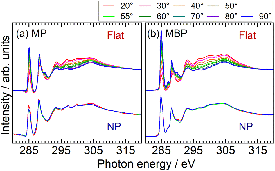 | ||
| Fig. 4 C K-edge NEXAFS spectra of the flat and NP films for (a) MP and (b) MBP molecules. Polarization angle dependence of spectra was investigated by altering the incident direction of the light from grazing (20°) to normal (90°). All spectra were normalized at the pre-edge and post-edge at 317 eV. Measurements for the flat films were taken at 10° intervals between 20° and 90°, as well as at the magic angle of 55°. Measurements for the NP films were performed at 20°, 55°, and 90°. | ||
The O K-edge NEXAFS spectra of the NP and flat films shown in Fig. 5 also exhibited identical spectral features, characteristic of molecules with methyl ester groups.42 Similar to that for the C K-edge NEXAFS spectra, the peaks appeared at the same energy positions for both the NP and flat films. In particular, three prominent peaks were observed: the first peaks for MP (at 531.7 eV) and MBP (at 531.5 eV) were assigned to O(CO) 1s → π*(CO) excitation, the second peaks for MP (at 534.3 eV) and MBP (at 533.9 eV) were assigned to O(OCH3) 1s → π*(CO) excitation, and the peaks at ∼540 eV were assigned to O(OCH3) 1s → σ*(C–OCH3) excitation. We focused on the O-excited CHC at the first π* peaks, for which the energies relative to the Fermi level were crucial for assessment. Considering the XPS data of O 1s (CO) binding energy of 531.7 eV for MP, which coincided with the π* excitation energy, the core-excited electron in the first π* orbital could move from molecules to substrates in the case of MP. Meanwhile, the first π* orbital of MBP is located 0.1 eV below the Fermi level by considering the O 1s (CO) binding energy of 531.6 eV, but electron transport may still be possible within the photon energy resolution.
 | ||
| Fig. 5 O K-edge NEXAFS spectra of the flat (red lines) and NP films (blue lines) for (a) MP and (b) MBP molecules. The incident angle was set to 55°. | ||
Thiolates adsorbed on the 7-nm-diameter AuNPs are expected to be less ordered than on a flat Au (111) surface. The AuNP surfaces are dominated by {111} terraces, rather than NP corners and edges.44 Alkanethiolates on AuNPs with particle sizes >4.4 nm have been reported to form “bundles” on the {111} terrace, forming SAMs similar to flat films.44–47 Based on these findings, an oriented monolayer, similar to that on a flat Au surface, is suggested to form on NP surfaces. Overall, the XPS and NEXAFS measurement results revealed that SAMs were identically formed on both the NP and flat surfaces, enabling the analysis of nuclear and electron dynamics within well-characterized molecule–metal interfaces.
Nuclear dynamics via resonant core excitation
Nuclear dynamics after resonant core excitation was investigated via soft X-ray spectroscopy. The core electron of a specific atom can be excited to an antibonding orbital localized to the adjacent bond, often resulting in selective chemical bond breaking. This is facilitated by the weakening of the bonding power by pumping the core electron into the antibonding orbital and by the Coulomb repulsion between the two holes created in the bonding orbital after the subsequent Auger decay.27 Such site-selective chemical bond breaking indicates nuclear dynamics that reflect the localized nature of core excitation and has been found in gaseous molecules28 and SAMs31 since its discovery by Eberhardt et al.26 In this study, site-selective ion desorption was measured for aromatic molecules adsorbed on NP and flat metal surfaces to demonstrate the local core excitation character.The ion desorption induced by resonant core excitation in the C K-edge region was studied via TOF-MS. As a representative example, TOF-MS spectrum of the MP flat films at 289 eV is shown in Fig. 6(a). Predominantly, the H+, H2+, and CHn+ (n = 0–3) ions desorbed from the films, whereas C2Hm+ (m = 0–5) and C3Hl+ (l = 0–7) ions were also detected as minor products. In conventional TOF measurements with single-bunch operation at the PF facility, all mass peaks were restricted within 624 ns.31 However, using the SR pulse selector solved this problem,38 allowing for clear detection of heavier- and weaker-mass peaks. Fig. 6(b) and (c) show the total ion yield (TIY) spectra and partial ion yield (PIY) spectra of H+ and CHn+ ions desorbed from the flat films at the C K-edge. The PIY spectra were obtained via integration of each mass peak of the TOF-MS spectra measured at various photon energies. The TIY and PIY spectra of the MP and MBP flat films exhibited similar features. The PIY spectra of the CHn+ ions showed single sharp peaks at 289 eV, corresponding to the site-selective desorption of CHn+ ions due to scission of the O–CH3 bond via C(OCH3) 1s → σ*(O–CH3) excitation, consistent with the characteristics observed for flat MHDA SAMs.30,31 However, such selectivity was not observed in the photodissociation of gaseous methyl benzoate molecules (similar to that for MP molecules)48 but was characteristic of adsorbed molecules. Compared with aliphatic MHDA SAMs, the site-selective ion desorption at the σ*(O–CH3) resonance occurred with violent fragmentation from the desorbed CH3+ ions, as shown in Fig. 6(a).31 The PIY spectra of H+ show peaks at the σ*(O–CH3) resonance, but the spectral shapes follow the absorption spectra rather than single peak shapes such as CHn+.31
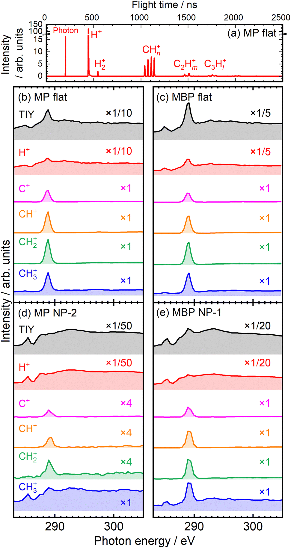 | ||
| Fig. 6 (a) TOF-MS spectra measured at 289 eV for MP flat films using an SR pulse selector. TIY and PIY spectra for the (b) MP flat, (c) MBP flat, (d) MP NP, and (e) MBP NP films. | ||
The ion yield spectra of the NP films are shown in Fig. 6(d) and (e). The PIY spectra of the C+, CH+, and CH2+ ions exhibited sharp peaks at 289 eV for both NP films, indicating site-selective ion desorption even in the condensed NP films, as observed in the case of the flat films. The CH3+ ion for MBP NP films also exhibited sharp peak at 289 eV, whereas the spectrum of the CH3+ ion for MP NP films notably differed and resembled the absorption-reflected H+ spectrum, seemingly decreasing the site-selectivity. Such differences might have arisen depending on the NP films prepared from different batches. Fig. 6(d) and (e) show representative examples of the poor selectivity of MP NP films and the satisfactory selectivity of MBP NP films, respectively. The opposite situation was also measured, as shown in Fig. S3 in the ESI,† where MP NP films retain satisfactory selectivity but MBP NP films lose selectivity. Thus, the PIY profiles sensitively represented the condensation conditions of NP films.
Such poor selectivity was attributed to increase in ion desorption indirectly caused via secondary processes. One process is delocalization of excess energy within a molecule via statistical energy redistribution. This relaxation can nonselectively cause ion desorption that is unrelated to the excitation site. This nonselective ion desorption results in a PIY profile that reflects the absorption intensity, with this effect being specifically pronounced in H+ ions, which desorb more easily.31 Another secondary process is bond scission induced by energetic photoelectrons and Auger electrons, commonly called X-ray-induced electron-stimulated desorption (XESD).31,49,50 This phenomenon is frequently observed in surface-condensed molecules. Such XESD also induces ion desorption depending on absorption intensity, as seen for condensed multilayer films of methyl isobutyrate molecules.29 In particular, these secondary processes might be prominent in condensed NP films.
The site-selective ion desorption was measured to some extent for both NP films, representing the combination of selective and nonselective desorption processes. The CH3+ PIY spectra of NP films depicted in Fig. 7 show variations due to different condensation conditions, where blue line in Fig. 7(a) is redrawn from Fig. S3(a) (ESI†), in Fig. 7(b) is from Fig. 6(e), in Fig. 7(c) is from Fig. 6(d), and in Fig. 7(d) is from Fig. S3(b) (ESI†). The PIY spectra in Fig. 7(a) and (b) were the case when satisfactory selectivity was observed, wheareas selectivity was lost in Fig. 7(c) and (d). As previously mentioned, the H+ PIY (red dotted lines) was used to represent the desorption via secondary processes. To extract the site-selective components of CH3+ PIY, we aligned H+ PIY at spectral intensities at 285 eV and above the IPs. The difference spectra depicted by black lines describe single peaks at the σ*(O–CH3) resonances, similar to that for the flat films. Through the analysis of CH3+ PIY, the site-selectivity for each film was estimated from the component ratios at 289 eV to be (a) 78% for the MP NP-1 films, (b) 69% for the MBP NP-1 films, (c) 39% for the MP NP-2 films, and (d) 30% for the MBP NP-2 films. These findings highlight that ultrafast nuclear dynamics, such as site-selective ion desorption induced by site-specific core excitation,31 occurs in the NP films despite these films having predominant secondary processes, and that site-selective components can be reflected in PIY.
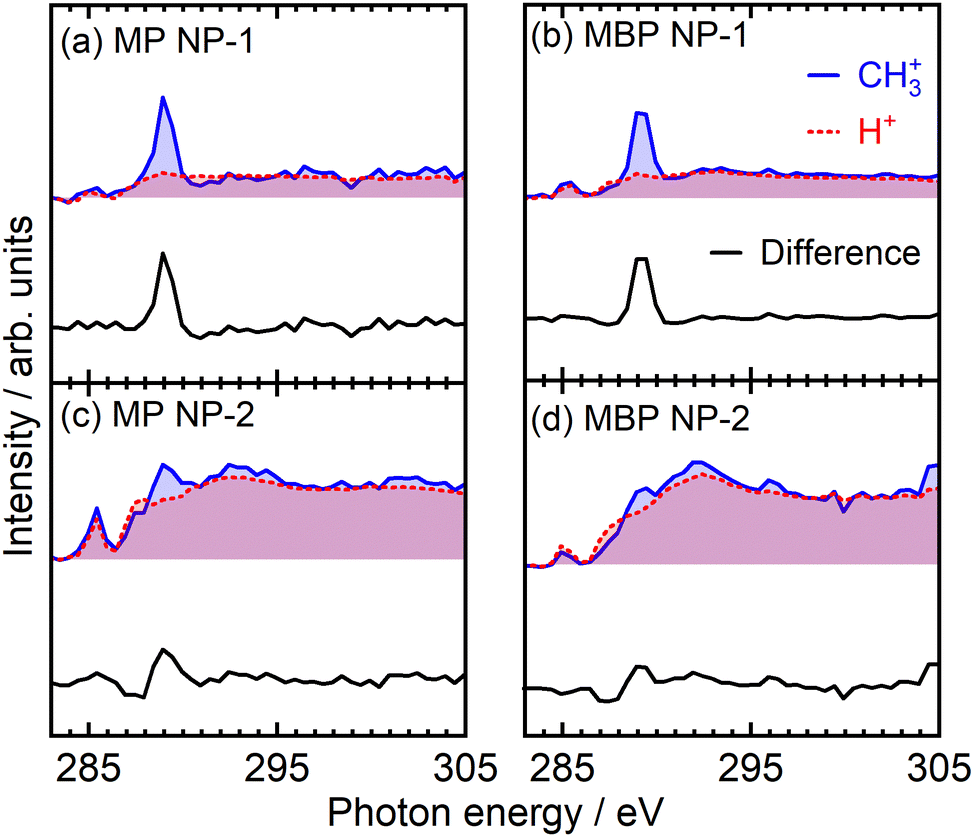 | ||
| Fig. 7 PIY spectra of CH3+ ions (blue lines) measured for MP ((a) and (c)) and MBP ((b) and (d)) NP films prepared from different batches. To extract the site-selective components of CH3+ PIY, the H+ PIY (red dotted lines) was aligned by matching the spectral intensities at 285 eV and above the IP. The difference spectra of CH3+ and H+ PIY, represented by black lines, correspond to the single site-selective peaks. | ||
Electron dynamics via resonant core excitation
RAES-CHC is a powerful tool for monitoring electron transport dynamics on the basis of the RAES spectral shape characteristics of various Auger decay processes. Resonant excitation is generally followed by spectator or participator Auger decay, resulting in emission of an Auger electron. If delocalization of the core-excited electron is allowed and the electron can be transported to the substrate within the core-hole lifetime, the resonant Auger decay and electron transport processes compete with each other. Thus, the Auger decay spectrum represents a combination of resonant Auger decay and electron transport contribution, with the latter corresponding to normal Auger decay and differing from the former in terms of spectral shape and position. To determine the branching ratio between resonant and normal Auger decay pathways, the spectrum was decomposed into a linear combination of the normal and pure resonant Auger spectra. The latter was obtained from a reference sample with negligible electron transport contribution.19 Consequently, the electron transport time could be derived from the branching ratio defined using the core-hole lifetime.
Fig. 8(a) shows the RAES spectra of the NP and flat films where the O(CO) 1s core electron was excited to the conjugated π*(CO) orbital at ∼532 eV. The nonresonant contributions were subtracted using the electron spectra recorded at 525 eV of pre-edge excitation. The RAES spectra are shown for the MP flat (red dots), MBP flat (orange dots), MP NP (green dots), and MBP NP films (blue dots). The spectral shapes of the NP and flat films were almost identical, representing the same final states overall. However, the NP films exhibited notably higher intensity around 460 eV compared with the flat films. This intensity difference was attributed to inelastic scattering due to condensed NPs and was accounted for by the Shirley background, represented by black lines.
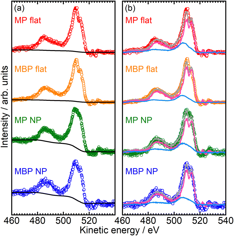 | ||
| Fig. 8 (a) RAES spectra for MP flat (red dots), MBP flat (orange dots), MP NP (green dots), and MBP NP (blue dots) films with Shirley's background represented by black lines. (b) RAES spectra after subtraction of Shirley's background were analyzed via a core-hole-clock approach. The pink and sky-blue lines represent the pure resonant and the normal Auger spectra, respectively. The gray lines represent the reproduced spectra obtained by summing the weighted pure resonant and normal Auger spectra. | ||
The background-subtracted RAES spectra of the NP and flat films shown in Fig. 8(b) were analyzed via the CHC approach. The fitted pure resonant Auger spectra represented by pink lines and the normal Auger spectra denoted by sky-blue lines are also depicted in the figure. The gray lines represent the reproduced spectra obtained via linear combination of the pure-resonant and normal Auger components. The analysis was conducted within the kinetic energy range of 460–517 eV. The normal Auger spectra were measured at 541 eV, which was considerably more than IPs. As the pure resonant Auger spectrum of the reference sample, we used the resonant Auger spectrum at O(C = O) 1s → π*(C = O) excitation for flat MHDA SAMs, in which methyl ester group as an X-ray absorption center is isolated from the metal substrates via the long and insulating methylene chains.23 The branching ratio of electron transport, PET, was obtained using the proportion of the normal Auger components. The PET values were determined to be 0.26 for the MP flat films, 0.20 for the MBP flat films, 0.27 for the MP NP films, and 0.20 for the MBP NP films. The following CHC analytical expression was used to express the electron transport time, τET, using PET:19
 O) resonance were determined to be 11 ± 3 fs for the MP flat films, 15 ± 4 fs for the MBP flat films, 10 ± 5 fs for the MP NP films, and 15 ± 6 fs for the MBP NP films. τET in both the NP and flat films was observed to increase with chain length, similar to the values reported by Zharnikov et al.19,24 report for flat films of aromatic SAMs with nitrile groups, as summarized in Table 1. Most importantly, the τET obtained in this study remained unchanged across the condensed NP and flat films.
Prior to examining the CHC results of the NP films, we discuss the electron transport dynamics in the flat films. τET was observed to exponentially increase with number of phenyl rings, nph:
| τET ∝ exp(βnph), |
The τET and β values of the NP films quantitatively agreed with those of the flat films. Even in environments where interactions between the molecules adsorbed on an NP itself or those on adjacent NPs cannot be ignored, such as in the condensed NP films, the electron transport process could be understood similarly to that in the flat films. These findings were supported by the fact that the spectral energy positions in the XPS and NEXAFS spectra remained unchanged. These results supported the validity of the through-bond electron transport model, in which electron transport was mediated via molecular orbitals, both for the condensed NP films and flat films.
We could explain the electron dynamics by subtracting the inelastic scattering processes. Compared with the flat films, increased background components were observed in the XPS, RAES, and PIY spectra of the condensed NP films. By elucidating the origin of these background components, we could successfully employ soft X-ray spectroscopy to understand electron transport for molecules on metal NP surfaces even under the condensation conditions of NP films.
Conclusions
Nuclear and electron dynamics at aromatic molecule–metal interfaces in condensed AuNP films was elucidated via soft X-ray excitation. The XPS and NEXAFS measurements revealed no notable differences in the chemical states and electronic structures of the aromatic molecules between NP and flat films. In both cases, the aromatic molecules formed SAMs on the metal surfaces, adopting an upright orientation relative to the metal surfaces. Ultrafast nuclear dynamics investigated using ion yield spectra revealed site-selective ion desorption via site-specific core excitation, similar to that observed in the flat films, even in condensed NP films where the secondary processes were dominant. The electron transport time of the condensed NP films was successfully determined via the RAES-CHC approach by subtracting the inelastic scattering components. Despite the presence of intermolecular interactions, the ultrafast electron transport in the NP films remained comparable to that of flat surfaces. The decay coefficients, which were consistent between NP and flat films, supported the through-bond transport model. Our results demonstrate the feasibility of evaluating electron transport and site-selective bond scission for molecules on metal NP surfaces by accounting for the inelastic scattering of electrons and secondary ion processes. The RAES-CHC results extend our understanding of electron transport properties from flat to NP films. These insights provide crucial information for optimizing electron transport properties in the design of next-generation NP-based materials, including molecular electronics, solar cells, biosensors, and memory devices.Data availability
The data supporting the findings of this study are included within the article and its supplementary materials. No additional datasets or code were generated or analyzed during the current study. If the publicly available information is not sufficient, the data for this article, including experimental data and spectral data are available at Hiroshima University at https://molphoto.hiroshima-u.ac.jp/research/2024NPtendo.html.Conflicts of interest
There are no conflicts to declare.Acknowledgements
This work was financially supported by JSPS KAKENHI (grants 19J21707, 26390019, 20K05420, 21K20538, and 22K14555). This work was performed under the approval of the Photon Factory Program Advisory Committee (Proposal No. 2021G095, 2023G050). The NEXAFS, XPS, and RAES measurements were performed with the approval of the Research Institute for Synchrotron Radiation Science (Proposal No. 21BG025, 22AG025, 22BG044). This study was supported in part by the Natural Science Center for Basic Research and Development (NBARD-00135) with an ultrahigh-resolution field-emission scanning electron microscope (Hitachi High-Technologies S-5200). The glass vessel used for pulsed laser ablation in liquid was manufactured at Monozukuri Plaza, Hiroshima University.References
- D. Morales-Martinez, F. Polo, S. Antonello and F. Maran, Electrochemically induced electron transfer through molecular bridges, Curr. Opin. Electrochem., 2021, 28, 100700 CrossRef CAS.
- J. Fujisawa, Interfacial Charge-Transfer Transitions for Direct Charge-Separation Photovoltaics, Energies, 2020, 13, 2521 CrossRef CAS.
- B. P. Bloom, R. Liu, P. Zhang, S. Ghosh, R. Naaman, D. N. Beratan and D. H. Waldeck, Directing Charge Transfer in Quantum Dot Assemblies, Acc. Chem. Res., 2018, 51, 2565–2573 CrossRef CAS.
- M. Hromadová and F. Vavrek, Electrochemical electron transfer and its relation to charge transport in single molecule junctions, Curr. Opin. Electrochem., 2020, 19, 63–70 CrossRef.
- A. Asaithambi, N. Kazemi Tofighi, M. Ghini, N. Curreli, P. J. Schuck and I. Kriegel, Energy transfer and charge transfer between semiconducting nanocrystals and transition metal dichalcogenide monolayers, Chem. Commun., 2023, 59, 7717–7730 RSC.
- V. Amendola, R. Pilot, M. Frasconi, O. M. Maragò and M. A. Iatì, Surface plasmon resonance in gold nanoparticles: a review, J. Phys.: Condens. Matter, 2017, 29, 203002 CrossRef PubMed.
- F. Xie, W. C. H. Choy, W. E. I. Sha, D. Zhang, S. Zhang, X. Li, C. Leung and J. Hou, Enhanced charge extraction in organic solar cells through electron accumulation effects induced by metal nanoparticles, Energy Environ. Sci., 2013, 6, 3372 RSC.
- A. Zabet-Khosousi and A.-A. Dhirani, Charge Transport in Nanoparticle Assemblies, Chem. Rev., 2008, 108, 4072–4124 CrossRef CAS PubMed.
- R. J. Nichols, W. Haiss, S. J. Higgins, E. Leary, S. Martin and D. Bethell, The experimental determination of the conductance of single molecules, Phys. Chem. Chem. Phys., 2010, 12, 2801 RSC.
- J. Xu, X. Tong, P. Yu, G. E. Wenya, T. McGrath, M. J. Fong, J. Wu and Z. M. Wang, Ultrafast Dynamics of Charge Transfer and Photochemical Reactions in Solar Energy Conversion, Adv. Sci., 2018, 5, 1800221 CrossRef.
- A. W. Snow and H. Wohltjen, Size-Induced Metal to Semiconductor Transition in a Stabilized Gold Cluster Ensemble, Chem. Mater., 1998, 10, 947–949 CrossRef CAS.
- A. W. Snow, M. G. Ancona, W. Kruppa, G. G. Jernigan, E. E. Foos and D. Park, Self-assembly of gold nanoclusters on micro- and nanoelectronic substrates, J. Mater. Chem., 2002, 12, 1222–1230 RSC.
- S. Kano, T. Tada and Y. Majima, Nanoparticle characterization based on STM and STS, Chem. Soc. Rev., 2015, 44, 970–987 RSC.
- R. Katoh, A. Furube, M. Kasuya, N. Fuke, N. Koide and L. Han, Photoinduced electron injection in black dye sensitized nanocrystalline TiO2 films, J. Mater. Chem., 2007, 17, 3190 RSC.
- H. S. Kato, Y. Murakami, Y. Kiriyama, R. Saitoh, T. Ueba, T. Yamada, Y. Ie, Y. Aso and T. Munakata, Decay of the Exciton in Quaterthiophene-Terminated Alkanethiolate Self-Assembled Monolayers on Au(111), J. Phys. Chem. C, 2015, 119, 7400–7407 CrossRef CAS.
- L. Wang, W. Chen and A. T. S. Wee, Charge transfer across the molecule/metal interface using the core hole clock technique, Surf. Sci. Rep., 2008, 63, 465–486 CrossRef CAS.
- P. A. Brühwiler, O. Karis and N. Mårtensson, Charge-transfer dynamics studied using resonant core spectroscopies, Rev. Mod. Phys., 2002, 74, 703–740 CrossRef.
- L. Cao, X. Gao, A. T. S. Wee and D. Qi, Quantitative Femtosecond Charge Transfer Dynamics at Organic/Electrode Interfaces Studied by Core-Hole Clock Spectroscopy, Adv. Mater., 2014, 26, 7880–7888 CrossRef CAS.
- M. Zharnikov, Femtosecond Charge Transfer Dynamics in Monomolecular Films in the Context of Molecular Electronics, Acc. Chem. Res., 2020, 53, 2975–2984 CrossRef CAS PubMed.
- P. Waske, T. Wächter, A. Terfort and M. Zharnikov, Nitro-Substituted Aromatic Thiolate Self-Assembled Monolayers: Structural Properties and Electron Transfer upon Resonant Excitation of the Tail Group, J. Phys. Chem. C, 2014, 118, 26049–26060 CrossRef CAS.
- W. Chen, L. Wang, C. Huang, T. T. Lin, X. Y. Gao, K. P. Loh, Z. K. Chen and A. T. S. Wee, Effect of Functional Group (Fluorine) of Aromatic Thiols on Electron Transfer at the Molecule−Metal Interface, J. Am. Chem. Soc., 2006, 128, 935–939 CrossRef CAS.
- T. Hellmann, C. S. Inagaki, M. F. F. Das Neves, M. M. Oliveira, L. S. Roman, A. J. G. Zarbin and M. L. M. Rocco, Preparation and characterization of polythiophene/gold nanoparticles/carbon nanotubes nanocomposites thin films: Spectroscopy and morphology, Mater. Today Commun., 2022, 33, 104314 CrossRef CAS.
- P. Kao, S. Neppl, P. Feulner, D. L. Allara and M. Zharnikov, Charge Transfer Time in Alkanethiolate Self-Assembled Monolayers via Resonant Auger Electron Spectroscopy, J. Phys. Chem. C, 2010, 114, 13766–13773 CrossRef CAS.
- H. Hamoudi, S. Neppl, P. Kao, B. Schüpbach, P. Feulner, A. Terfort, D. Allara and M. Zharnikov, Orbital-Dependent Charge Transfer Dynamics in Conjugated Self-Assembled Monolayers, Phys. Rev. Lett., 2011, 107, 027801 CrossRef CAS.
- F. Blobner, P. B. Coto, F. Allegretti, M. Bockstedte, O. Rubio-Pons, H. Wang, D. L. Allara, M. Zharnikov, M. Thoss and P. Feulner, Orbital-Symmetry-Dependent Electron Transfer through Molecules Assembled on Metal Substrates, J. Phys. Chem. Lett., 2012, 3, 436–440 CrossRef CAS.
- W. Eberhardt, T. K. Sham, R. Carr, S. Krummacher, M. Strongin, S. L. Weng and D. Wesner, Site-Specific Fragmentation of Small Molecules Following Soft-X-Ray Excitation, Phys. Rev. Lett., 1983, 50, 1038–1041 CrossRef CAS.
- S. Wada, in Encyclopedia of Interfacial Chemistry, ed. K. Wandelt, Elsevier, Oxford, 2018, pp. 621–628 Search PubMed.
- Y.-J. Chiang, W.-C. Huang, C.-H. Han, C.-L. Liu, C.-C. Tsai and W.-P. Hu, Near-edge x-ray absorption fine structure spectra and specific dissociation of small peptoid molecules, J. Chem. Phys., 2024, 160, 074305 CrossRef CAS.
- S. Wada, R. Sumii, K. Isari, S. Waki, E. O. Sako, T. Sekiguchi, T. Sekitani and K. Tanaka, Active control of chemical bond scission by site-specific core excitation, Surf. Sci., 2003, 528, 242–248 CrossRef CAS.
- S. Wada, R. Sumii, H. Kizaki, Y. Iizuka, Y. Matsumoto, T. Sekitani and K. Tanaka, Ion desorption of surface-oriented methyl-ester compounds using a self-assembled monolayer by core-electron excitations: Polarization-dependence measurements, Surf. Sci., 2005, 593, 283–290 CrossRef CAS.
- S. Wada, H. Kizaki, Y. Matsumoto, R. Sumii and K. Tanaka, Selective chemical bond breaking characteristically induced by resonant core excitation of ester compounds on a surface, J. Phys.: Condens. Matter, 2006, 18, S1629 CrossRef CAS.
- J. F. Watts and J. Wolstenholme, An Introduction to Surface Analysis by XPS and AES, John Wiley & Sons, Hoboken, 2005 Search PubMed.
- J. Stöhr, NEXAFS Spectroscopy, Springer Berlin Heidelberg, Berlin, Heidelberg, 1992, vol. 25 Search PubMed.
- W.-Y. Rho, D. H. Song, H.-Y. Yang, H.-S. Kim, B. S. Son, J. S. Suh and B.-H. Jun, Recent advances in plasmonic dye-sensitized solar cells, J. Solid State Chem., 2018, 258, 271–282 CrossRef CAS.
- J.-S. Lee, Recent progress in gold nanoparticle-based non-volatile memory devices, Gold Bull., 2010, 43, 189–199 CrossRef.
- D. Zhang, B. Gökce and S. Barcikowski, Laser Synthesis and Processing of Colloids: Fundamentals and Applications, Chem. Rev., 2017, 117, 3990–4103 CrossRef CAS.
- R. Püttner, I. Dominguez, T. J. Morgan, C. Cisneros, R. F. Fink, E. Rotenberg, T. Warwick, M. Domke, G. Kaindl and A. S. Schlachter, Vibrationally resolved O 1 s core-excitation spectra of CO and NO, Phys. Rev. A: At., Mol., Opt. Phys., 1999, 59, 3415–3423 CrossRef.
- B. Watts, L. Thomsen and P. C. Dastoor, A simple polarimeter for quantifying synchrotron polarization, J. Electron Spectrosc. Relat. Phenom., 2006, 151, 208–214 CrossRef CAS.
- D. Vaughan, X-Ray Data Booklet. Center for X-Ray Optics, Lawrence Berkeley National Laboratory, 1985.
- J. Adachi, H. Tanaka, T. Kosuge, H. Ishii, I. H. Suzuki, T. Kaneyasu, T. Taniguchi, T. Odagiri, S. Ohtaki, Y. Tsuji, K. Soejima, P. Lablanquie and Y. Hikosaka, Development of pulse selectors for the synchrotron radiation pulses from the Photon Factory 2.5 GeV ring to study multiple photoionization, J. Phys.: Conf. Ser., 2020, 1412, 152092 CrossRef.
- A. P. Hitchcock, P. Fischer, A. Gedanken and M. B. Robin, Antibonding σ* valence MOs in the inner-shell and outer-shell spectra of the fluorobenzenes, J. Phys. Chem., 1987, 91, 531–540 CrossRef CAS.
- O. Takahashi, K. Tabayashi, S. Wada, R. Sumii, K. Tanaka, M. Odelius and L. G. M. Pettersson, Theoretical study of ion desorption from poly-(methyl methacrylate) and poly-(isopropenyl acetate) thin films through core excitation, J. Chem. Phys., 2006, 124, 124901 CrossRef.
- I. Bâldea, B. Schimmelpfennig, M. Plaschke, J. Rothe, J. Schirmer, A. B. Trofimov and T. Fanghänel, C 1s near edge X-ray absorption fine structure (NEXAFS) of substituted benzoic acids—A theoretical and experimental study, J. Electron Spectrosc. Relat. Phenom., 2007, 154, 109–118 CrossRef.
- J. C. Love, L. A. Estroff, J. K. Kriebel, R. G. Nuzzo and G. M. Whitesides, Self-Assembled Monolayers of Thiolates on Metals as a Form of Nanotechnology, Chem. Rev., 2005, 105, 1103–1170 CrossRef CAS.
- A. Badia, L. Cuccia, L. Demers, F. Morin and R. B. Lennox, Structure and Dynamics in Alkanethiolate Monolayers Self-Assembled on Gold Nanoparticles: A DSC, FT-IR, and Deuterium NMR Study, J. Am. Chem. Soc., 1997, 119, 2682–2692 CrossRef CAS.
- W. D. Luedtke and U. Landman, Structure, Dynamics, and Thermodynamics of Passivated Gold Nanocrystallites and Their Assemblies, J. Phys. Chem., 1996, 100, 13323–13329 CrossRef CAS.
- W. D. Luedtke and U. Landman, Structure and Thermodynamics of Self-Assembled Monolayers on Gold Nanocrystallites, J. Phys. Chem. B, 1998, 102, 6566–6572 CrossRef CAS.
- O. Takahashi, K. Kooser, D. T. Ha, H. Myllynen, J. Laksman, E. Rachlew and E. Kukk, Site-selective bond scission of methylbenzoate following core excitation, Phys. Chem. Chem. Phys., 2018, 20, 9591–9599 RSC.
- R. Jaeger, J. Stöhr and T. Kendelewicz, Ion desorption from surfaces following photon excitation of core electrons in the bulk, Phys. Rev. B: Condens. Matter Mater. Phys., 1983, 28, 1145–1147 CrossRef CAS.
- D. Coulman, A. Puschmann, U. Höfer, H.-P. Steinrück, W. Wurth, P. Feulner and D. Menzel, Excitation, deexcitation, and fragmentation in the core region of condensed and adsorbed water, J. Chem. Phys., 1990, 93, 58–75 CrossRef CAS.
- C. Nicolas and C. Miron, Lifetime broadening of core-excited and -ionized states, J. Electron Spectrosc. Relat. Phenom., 2012, 185, 267–272 CrossRef CAS.
- S. Karthäuser, Control of molecule-based transport for future molecular devices, J. Phys.: Condens. Matter, 2011, 23, 013001 CrossRef.
- L. Cao, Z. Zhang, D. Thompson, D.-C. Qi and C. A. Nijhui, Resolving charge transfer mechanisms in molecular tunnel junctions using dynamic charge transfer and static current–voltage measurements, J. Mater. Chem. C, 2024, 12, 1701–1709 RSC.
Footnotes |
| † Electronic supplementary information (ESI) available. See DOI: https://doi.org/10.1039/d4cp03556a |
| ‡ Present affiliation of Akinobu Niozu: Graduate School of Humanities and Social Sciences, Hiroshima University, Higashi-Hiroshima 739-8524, Japan. |
| This journal is © the Owner Societies 2025 |