
Optimization of active layers for efficient binary organic solar cells†
Yunjie
Li‡
ab,
Beining
Wang‡
b,
Lijun
Chen
b,
Yaqian
Yuan
c,
Jianfei
Fu
b,
Chong
Geng
 c,
Junmin
Wan
*a and
Hai-Qiao
Wang
*b
c,
Junmin
Wan
*a and
Hai-Qiao
Wang
*b
aSchool of Materials Science and Engineering, Zhejiang Sci-Tech University, Hangzhou, China. E-mail: wwjm2001@126.com
bZhejiang Engineering Research Center for Fabrication and Application of Advanced Photovoltaic Materials, School of Materials Science and Engineering, NingboTech University, Ningbo 315100, China. E-mail: hqwang@nbt.edu.cn
cSchool of Electronics and Information Engineering, Hebei University of Technology, Tianjin 300401, China
First published on 29th November 2024
Abstract
The photovoltaic performance of organic solar cells (OSCs) is closely related to the active layer and its microstructure. Therefore, it is essential to coordinately control the preparation process parameters from multiple perspectives to optimize the morphology and improve the device's photovoltaic performance. Based on the classical and efficient PM6:L8-BO active system, this paper systematically studies the effects of annealing temperature, film thickness, solvent additives, and other factors on the film microstructure, exciton generation and dissociation, charge transport, phase separation, and light absorption. The results show that an annealing temperature of 90 °C and the solvent additive diiodooctane (DIO) maximize the optimization of the micromorphology of the active layer. Finally, a champion conversion efficiency (PCE) of 18.33% was achieved for binary OSCs, under the condition of an active layer thickness of 100 nm, with an open-circuit voltage (Voc) of 0.881 V, a short-circuit current density (Jsc) of 26.56 mA cm−2 and a fill factor (FF) of 78.33%.
Introduction
Organic solar cells (OSCs) have garnered significant attention from the photovoltaic research community due to their numerous advantages, including flexibility, a wide absorption spectrum, lightweight, low cost, and excellent thermal stability.1–4 In recent years, the development of new active layers and interface materials has propelled the rapid advancement of OSCs, continually setting new records for power conversion efficiency (PCE).4,5 For instance, the PM6-L8-BO active system can be easily processed by different solvent systems and deliver high power conversion efficiency (PCE), which has gained great attention from the community.6–9 Efficiencies of over 18% and over 19% have been reported for binary10 and ternary7 PM6-L8-BO solar cells, respectively. The recently published research works on this active system have been summarized in the discussion part for comparison.The bulk heterojunction (BHJ) structure is the most employed active layer configuration in OSCs, wherein donor and acceptor materials are mixed at the nanoscale to create a double continuous interpenetrating network that facilitates efficient exciton dissociation and charge transport.11,12 Binary or ternary methods13,14 and additive strategies15 have usually been applied to prepare the BHJ active layer, to tune and optimize the BHJ morphology and device's performance. To enhance the performance of OSCs, researchers have optimized various aspects, including the development of new photoactive materials,16–18 solvent selection,19–21 and interface22,23 and electrode24–26 optimization. However, the PCE of OSCs is predominantly determined by the light absorption performance of the active layer, the efficiency of exciton generation and dissociation, charge transport efficiency, and charge collection efficiency. Therefore, optimizing the active layer is crucial for improving device performance. Current optimization strategies for the active layer involve additives, solvents, temperature control, and adjustments to morphology, structure, thickness,27 and phase separation.28–31 Thus, it is essential to systematically and synergistically regulate OSC performance through multiple parameters.
Studying the influence of the active layer on device performance from the perspective of fundamental preparation techniques is highly meaningful.32 Morphological control by solvent/solid additives and morphology optimization by postdeposition treatment with thermal annealing and/or solvent vapour annealing have been extensively studied.32 They demonstrate promising positive effects in optimizing the morphology. To the best of our knowledge, few similar studies investigate this topic from multiple perspectives. This comprehensive approach is crucial for advancing the OSC field and supporting its industrialization.
This study is focused on a classical and efficient active system, i.e. using semiconducting polymer PM6 as the donor and non-fullerene L8-BO as the acceptor, in a normal device architecture of ITO/PEDOT/PM6:L8-BO/PDINN/Ag. We investigated the performance of OSCs by varying the thickness of the active layer, annealing temperature, and solvent additives. Additionally, we compared the effects of the layer-by-layer (LBL) manufacturing process on charge transport and extraction. The optimized active layer thickness was 100 nm, the annealing temperature was 90 °C, and OSCs with 0.5% DIO added to the PM6 blend solution exhibited the best photovoltaic performance. Specifically, these OSCs achieved a PCE of 18.33%, an open-circuit voltage (Voc) of 0.881 V, a short-circuit current density (Jsc) of 26.56 mA cm−2, and a fill factor (FF) of 78.33%. The results demonstrate that additives, optimizing the active layer thickness, and employing thermal annealing are effective methods for enhancing the photovoltaic performance of PM6:L8-BO non-fullerene system OSCs.
Results and discussion
Fig. 1a shows the schematic diagram of the device structure ITO/PEDOT/PM6:L8-BO/PDINN/Ag. A donor (PM6) and an acceptor (L8-BO) were selected and used in this work, and the chemical structures of the polymer PM6 and L8-BO are shown in Fig. 1c. A clear energy arrangement is formed between the different layers, which is conducive to effective charge transfer, as illustrated in the energy level diagram in Fig. 1b. Additionally, the UV-vis absorption spectra of the solution samples of PM6, L8-BO, and PM6:L8-BO are displayed in Fig. 2a. The pure PM6 solution sample exhibits absorbance in the 300 nm to 700 nm range, with an absorption peak at 630 nm. The L8-BO solution sample shows absorbance in the 300 nm to 800 nm range, with absorption peaks at 610 nm and 730 nm. The PM6:L8-BO solution sample exhibits complementary absorptions, similar to the overlap of the spectra of PM6 and L8-BO. However, compared to the solution sample, the PM6:L8-BO film prepared by spin coating from a chloroform solution shows an increased absorption coefficient and a redshift. The addition of DIO causes the absorption peak to shift further to the red and increases the absorption coefficient, indicating that thermal annealing and additives play a key role in the performance of the active layer (Fig. 2b). | ||
| Fig. 1 (a) Schematic device structure of the BHJ OSC. (b) Energy-level alignment of the materials used in the device. (c) Chemical structure of polymer donor PM6 and non-fullerene acceptor L8-BO. | ||
 | ||
| Fig. 2 (a) Absorption spectra of the pure PM6, L8-BO and mixture solutions dissolved in CF. (b) Absorption spectra of the PM6:L8-BO films with and without DIO additives. | ||
First, we studied the effect of active layer annealing temperature on the photovoltaic performance of the device, since thermal annealing could influence the crystallization and morphology of the active layer,33 thus affecting device efficiency. We compared annealing temperatures of 70, 90, and 110 °C for PM6:L8-BO thin films (Fig. 3a and d). With the thermal annealing temperature increased from 70 °C to 90 °C, a slight increase of Voc (from 0.86 V to 0.90 V) and Jsc (from 24.15 to 25.47 mA cm−2) was observed (Table 1). However, when the temperature increased to 110 °C, the FF got decreased and resulted in a decrease in PCE (from 15.25 to 13.7%). These parameters’ variations could be attributed to the morphology change of the active layer by different annealing temperatures.33 The results demonstrated that 90 °C annealing is suitable for the active layer, which is consistent with the results in the literature.34
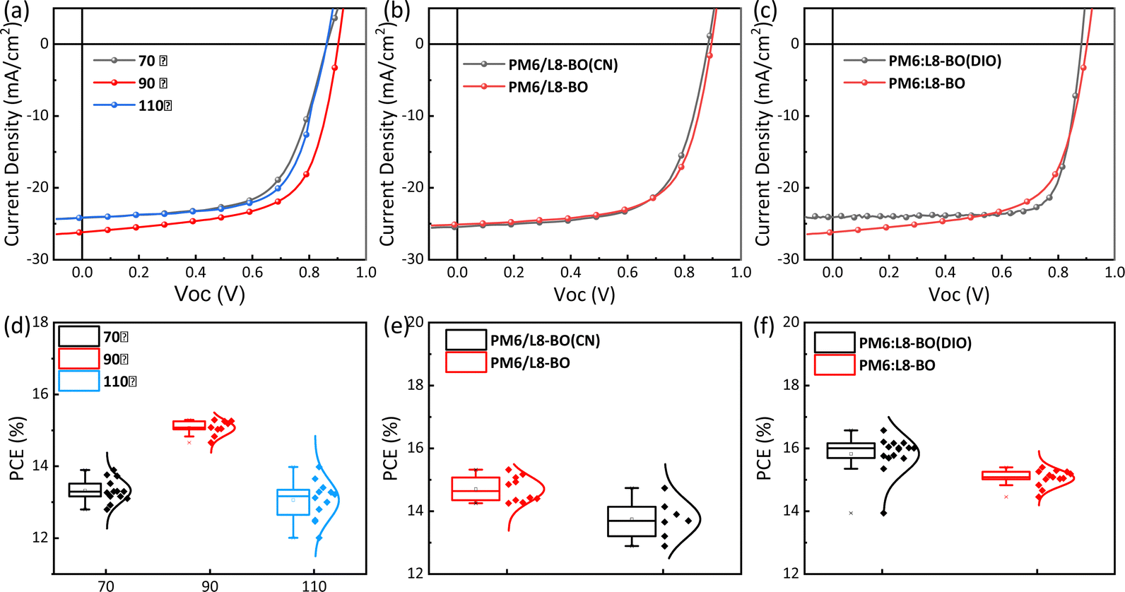 | ||
| Fig. 3 (a) J–V curves and (d) efficiency statistics of the BHJ OSCs with active layer treated at 70, 90 and 110 °C. (b) J–V curves and (e) efficiency statistics of the LBL OSCs with and without CN additives. (c) J–V curves and (f) efficiency statistics of the BHJ OSCs with and without DIO additives. | ||
| Conditions | V oc (V) | J sc (mA cm−2) | FF (%) | PCE (%) | |
|---|---|---|---|---|---|
| Annealing temperature (°C) | 70 | 0.861 (0.86 ± 0.01) | 24.15 (23.82 ± 0.40) | 66.82 (65.41 ± 2.50) | 13.90 (13.37 ± 0.40) |
| 90 | 0.900 (0.937 ± 0.01) | 25.47 (25.32 ± 0.50) | 66.82 (66.36 ± 0.60) | 15.25 (15.08 ± 0.20) | |
| 110 | 0.890 (0.8908 ± 0.01) | 25.34 (25.19 ± 0.30) | 60.77 (59.69 ± 1.8) | 13.70 (13.41 ± 0.50) | |
| Active layer configuration | PM6:L8-BO | 0.900 (0.9 ± 0.003) | 26.18 (25.52 ± 0.49) | 67.46 (65.74 ± 0.98) | 15.39 (15.05 ± 0.26) |
| PM6:L8-BO (0.5% DIO) | 0.870 (0.87 ± 0.01) | 25.58 (24.65 ± 0.50) | 76.77 (74.66 ± 2.59) | 16.88 (15.96 ± 0.70) | |
| PM6/L8-BO | 0.880 (0.87 ± 0.01) | 26.13 (25.21 ± 0.58) | 66.53 (62.75 ± 2.45) | 14.42 (13.74 ± 0.55) | |
| PM6/L8-B0 (0.5% CN) | 0.880 (0.88 ± 0.01) | 25.44 (24.89 ± 0.35) | 65.47 (62.86 ± 1.96) | 14.74 (13.75 ± 0.61) | |
| Active layer thickness (nm) | 96 | 0.880 (0.86 ± 0.01) | 25.7 (25.17 ± 0.39) | 78.22 (73.72 ± 3.27) | 17.42 (16.04 ± 1.08) |
| 100 | 0.881 (0.87 ± 0.01) | 26.61 (25.65 ± 0.82) | 78.36 (76.04 ± 1.50) | 18.33 (17.06 ± 0.57) | |
| 112 | 0.882 (0.87 ± 0.01) | 24.06 (23.94 ± 0.33) | 78.1 (75.72 ± 2.46) | 16.57 (15.82 ± 0.59) | |
Based on this optimal annealing temperature, we studied the performance of BHJ type and LBL type devices, respectively. As shown in Table 1, obvious differences in performance are observed for the BHJ and LBL devices. For the BHJ type, Voc of 0.900 V (0.9 ± 0.003), Jsc of 26.18 mA cm−2 (25.52 ± 0.49), FF of 67.46% (65.74 ± 0.98) and PCE of 15.39% (15.05 ± 0.26) are recorded, compared to Voc of 0.880 V (0.87 ± 0.01), Jsc of 26.13 mA cm−2 (25.21 ± 0.58), FF of 66.53% (62.75 ± 2.45) and PCE of 14.42% (13.74 ± 0.55) for the LBL type. The relative J–V curve and statistical data of the LBL device are presented in Fig. 3b and e. The BHJ type demonstrates higher efficiency based on this structure. To further optimize photovoltaic performance, we explored the effect of additives on device performance.6 Here, two additives are compared: a solvent additive DIO6 with a volume ratio of 0.5% added to the BHJ type active layer solution, and 0.5% chloronaphthalene (CN)35 added to the L8-BO acceptor solution in the LBL type. The results show that adding 0.5% DIO to the BHJ-type device resulted in better photovoltaic performance, particularly with a significantly improved FF (from 67.46% to 76.77%) (Table 1). It should be noted that the CN additive shows only a slight effect on the device performance (Table 1 and Fig. 3b, e) in our study. Based on the observations, it could be concluded that the BHJ PM6:L8-BO devices tend to provide better efficiency than the LBL PM6/L8-BO devices in our study, especially with DIO additives.
To further enhance device performance, we systematically investigated the impact of the BHJ active layer thickness on device efficiency.36 Active layer thicknesses of 90, 100 and 110 nm were confirmed, respectively, for three different cells (Fig. S1, ESI†). The results indicate that an active layer thickness of approximately 100 nm yields optimal performance parameters (Fig. 4a, b and Table 1), compared to that of 90 and 110 nm. At this optimal thickness, the device achieves a PCE of 18.33%, with a Voc of 0.88 V, a Jsc of 26.61 mA cm−2, and a champion PCE of 18.33% (Fig. 4c). Additionally, the maximum power point (MPP) test demonstrates excellent stability (Fig. S2 and S4, ESI†). For comparison, Table 2 provides the representative performance data of binary or ternary PM6:L8-BO solar cells reported in the literature. The ternary solar cells present slightly higher PCE than binary cells but involve more complex and costly processes. A device using PNDIT-F3N as the electron transporting layer (ETL) in a binary system achieves a PCE of 18.44%,7 which is marginally higher than our results. However, PNDIT-F3N is more expensive than PDINN used in our study. Consequently, our work demonstrates highly efficient binary organic solar cells through simple processes and cost-effective optimization, offering valuable insights for advancing industrial applications.
 | ||
| Fig. 4 (a) J–V curves and (b) efficiency statistics of the BHJ OSCs with 96, 100, and 112 nm thick active layer and DIO additives. (c) J–V curve of the device with champion performance. | ||
| Active layer | Additive | HTL | ETL | V oc (V) | J sc (mA cm−2) | FF (%) | PCE (%) | Ref. | |
|---|---|---|---|---|---|---|---|---|---|
| Ternary | PM6:L8-BO:DY-TF | — | PEDOT:PSS | PNDIT-F3N | 0.905 | 26.93 | 78.50 | 19.13 | AM 20237 |
| PM6:L8-BO:BR-C12 | — | PEDOT:PSS | PDINO | 0.881 | 26.66 | 77.72 | 18.26 | Dyes and Pigments 202337 | |
| PM6:L8-BO:BTP-eC9 | Th-BrSi | PEDOT:PSS-TA | PFN-Br-MA | 0.886 | 27.22 | 0.795 | 19.17 | AFM 20248 | |
| Binary | PM6:L8-BO | — | PEDOT:PSS-TA | PFN-Br-MA | 0.911 | 26.03 | 0.747 | 17.71 | AFM 20248 |
| PM6:L8-BO | Th-FSi | PEDOT:PSS-TA | PFN-Br-MA | 0.907 | 25.85 | 0.744 | 17.44 | AFM 20248 | |
| PM6:L8-BO | Th-ClSi | PEDOT:PSS-TA | PFN-Br-MA | 0.897 | 26.28 | 0.776 | 18.29 | AFM 20248 | |
| PM6:L8-BO | Th-BrSi | PEDOT:PSS-TA | PFN-Br-MA | 0.885 | 26.01 | 0.771 | 17.81 | AFM 20248 | |
| PM6:L8-BO | — | PEDOT:PSS | PFN-Br | 0.885 | 26.25 | 78.47 | 18.18 | AM 202210 | |
| PM6:L8-BO | — | PEDOT:PSS | PNDIT-F3N | 0.884 | 26.40 | 79.03 | 18.44 | AM 20237 | |
| PM6:L8-BO | DIO | PEDOT:PSS | PNDIT-F3N | 0.869 | 26.35 | 79.6 | 18.23 | Matter 20216 | |
| PM6:L8-BO | — | 2PACZ | PNDIT-F3N | 0.881 | 25.88 | 77.0 | 17.56 | Angewandte Chemie 20249 | |
| PM6:L8-BO | — | PEDOT:PSS | PDINO | 0.873 | 26.47 | 75.83 | 17.52 | Dyes and Pigments 202337 | |
| PM6:L8-BO | DIO | PEDOT:PSS | PDINN | 0.881 | 26.61 | 78.36 | 18.33 | This work | |
To understand why additives help improve performance, we conducted a series of characterization methods on BHJ devices with and without additives in the active layer. As described earlier, UV-ultraviolet absorption measurements show that the addition of the additive DIO causes a red shift and enhanced intensity in the absorption peak of the PM6:L8-BO film in the long-wavelength (800–850 nm). This suggests that the additive influences film formation and phase separation, which may significantly improve the fill factor (FF) and PCE. To further investigate changes in film morphology and microstructure, we performed AFM tests (Fig. 5). The root mean square roughness (Rq) increases from 1.07 nm to 4.86 nm after adding DIO to the PM6:L8-BO film (panels a and b, first column). Both films exhibit good nanofiber morphology as shown in the phase images (second column). However, the addition of DIO to the blend results in increased aggregation, as demonstrated by the increased Rq in the height image and slightly larger fiber size in the phase image. Combined with the 3D height image (the third column), roughly tens of nanometers of domain size can be estimated from the AFM result for the film with DIO additives, compared to the size of a few nanometers of the film without DIO. This could evidence the more suitable domain size of the polymers by DIO, beneficial the exciton dissociation and charge transfer, which could explain the relatively high-performance parameters of the device with DIO, as listed in Table 1. Elemental mapping by EDS was also applied to understand the film morphology and phase separation in active layers (Fig. S5 and S6, ESI†). However, it is difficult to provide detailed information for donor/acceptor distribution. Further, enhanced photoluminescence was recorded on the active layer with DIO (Fig. S7, ESI†), verifying depressed defect states in the active blend by DIO additives. It is believed that the addition of DIO can alter the crystallization state, surface roughness and domain size of the active layer. By which it could enhance carrier migration and charge transport.15
 | ||
| Fig. 5 AFM height, phase and 3D image of PM6:L8-BO blends without (a) and with (b) DIO additives. | ||
Moreover, to investigate the charge transport performance in the active layer films, we examined the photoinduced charge-transfer dynamics in PM6:L8-BO and PM6:L8-BO (DIO) films using time-resolved femtosecond transient absorption (TA) spectroscopy.38 The TA spectra primarily feature two negative characteristic peaks: the ground state bleaching (GSB) peak and the stimulated (SE) peak. As shown in Fig. 6a and b, to analyze the TA of the films, a specific 400 nm laser was chosen to pump the samples. This wavelength effectively excites the PM6 donor while minimally exciting the acceptor L8-BO (Fig. 2a). The TA spectra of both PM6:L8-BO and PM6:L8-BO (DIO) films show GSB peaks centred at approximately 630 nm, consistent with the stable absorption spectrum of PM6, with no noticeable ESA peak. No obvious signal between 700–750 nm (corresponding to L8-BO) was recorded for either film, due to the weak absorption of the 400 nm pump light. However, clear peaks in this range are evident in the TA spectra of PM6:L8-BO (DIO) within 1–60 ps (Fig. 6a) compared to those of PM6:L8-BO without DIO. This suggests that the presence of DIO facilitates charge transfer from PM6 to L8-BO. The faster decay rate of TA at 630 nm further confirms the enhanced energy/electron transfer from PM6 to L8-BO in the blend film with DIO additive (Fig. 6c). The TA spectra of the PM6 in the PM6:L8-BO(DIO) system display a rapid decay within 50 ps, indicating energy transfer from PM6 to L8-BO.
 | ||
| Fig. 6 TA spectra of PM6:L8-BO (a) and PM6:L8-BO (DIO) (b) films at indicated delay times. (c) The energy transfer processes of the films. | ||
Additionally, we utilized grazing incidence wide-angle X-ray scattering (GIWAXS) to investigate the impact of the additive on the molecular stacking and crystallinity of the active layer films. Both the PM6:L8-BO and PM6:L8-BO (DIO) films exhibit prominent (010) and (100) diffraction peaks in the in-plane (IP) and out-of-plane (00P) directions. Specifically, a (010) π–π stacking peak is observed along the OOP direction at qz = 1.73 Å−1, and a lamellar peak along the IP direction (100) is found at qxy = 0.282 Å−1 (Fig. 7b). The PM6:L8-BO film with DIO additives shows slightly enhanced absorption intensity (Fig. 7a) and denser molecular stacking, which facilitates charge transfer and exciton diffusion, thereby improving photovoltaic performance.
 | ||
| Fig. 7 GIWAXS 2D patterns (a) and 1D line-cuts (b) for PM6:L8-BO films with and without DIO additives. | ||
Conclusions
We prepared organic solar cells using an active layer system of PM6:L8-BO and conducted a detailed study on the effects of thermal annealing, additive treatment, and active layer thickness on performance. Optimal binary OSCs with a PCE of 18.33% were achieved with a Voc of 0.881 V, a Jsc of 26.56 mA cm−2 and an FF of 78.33%, by simple processes and cost-effective interfacial materials. The characterization results of AFM, GIWAXS, etc. indicate that incorporating additives into the active layer, applying thermal annealing at an appropriate temperature, and regulating the thickness can effectively optimise the active layer morphology, enhance charge transport and extraction, balance light absorption, and improve the interface contact between the active layer and the electrode, ultimately boosting the photovoltaic performance of PM6:L8-BO solar cells.Methods
Materials
Patterned ITO glass substrates (Rs ≤ 10 Ω □−1, T% ≥ 83%) were provided by Shenzhen huayulianhe Technology Co. The materials poly[(2,6-(4,8-bis(5-(2-ethylhexyl-3-fluoro)thiophen-2-yl)-benzo[1,2-b:4,5-b′]dithiophene))-alt-(5,5-(1′,3′-di-2-thienyl-5′,7′-bis(2-ethylhexyl)benzo[1′,2′-c:4′,5′-c′]dithiophene-4,8-dione))] (PM6), L8-BO and PDINN were obtained from Solarmer Materials Inc. The hole transporting material PEDOT:PSS was obtained from Xi’an Polymer Light Technology Corp. Chloroform (CF) was bought from Sigma-Aldrich. All the available chemical reagents were used as received without any further purification.(i) PM6:L8-BO bulk heterojunction (BHJ) with a concentration of 18 mg mL−1 (D![[thin space (1/6-em)]](https://www.rsc.org/images/entities/char_2009.gif) :A = 1:1.2);
:A = 1:1.2);
(ii) PM6:L8-BO BHJ with a concentration of 18 mg mL−1, incorporating 0.5 vol% 1,8-diiodooctane (DIO).
(iii) Layer-by-layer (LBL) device with a donor PM6 concentration of 12.5 mg mL−1 and an acceptor L8-BO concentration of 15 mg mL−1.
(iv) Similar to configuration 3, but with the addition of 0.5 vol% chloronaphthalene (CN) to the L8-BO solution.
Characterization
The thickness of the active layer film was measured using an AlphaStep D-12 step profiler. A UV-visible spectrophotometer was employed to assess the light absorption properties of the active layer film. Photovoltaic performance was characterized under the AM1.5G simulated solar spectrum using a Keithley K2450 source meter and a Sirius-SS300A-D solar simulator, calibrated with a certified standard silicon solar cell. The roughness and phase images of the active layer film were obtained using atomic force microscopy (AFM). Lateral and vertical molecular stacking of the active layer film was analyzed using a GIWAXS small-angle diffractometer (Xeuss 2.0).Data availability
The data supporting this article have been included as part of the ESI.†Conflicts of interest
There are no conflicts to declare.Acknowledgements
The authors acknowledge the financial support from the Zhejiang Provincial Natural Science Foundation of China (LY23F040004), the Ningbo Key Scientific and Technological Project (2022Z117), the Ningbo Science and Technology Project (2022-DST-004), the Ningbo Nature Science Foundation (2023J039) and the Joint University Education Program between China and Central and Eastern European Countries (2023268).References
- G. Zhang, J. Zhao, P. C. Y. Chow, K. Jiang, J. Zhang, Z. Zhu, J. Zhang, F. Huang and H. Yan, Chem. Rev., 2018, 118, 3447–3507 CrossRef CAS PubMed.
- Y. Lin, H. Skaff, T. Emrick, A. D. Dinsmore and T. P. Russell, Science, 2003, 299, 226–229 CrossRef CAS.
- Z. Yin, H. Zhao, Y. Liu, X. Xiao, Y. Zhang, H. Lai, N. Li and H.-Q. Wang, Energy Environ. Mater., 2024, 7, e12665 CrossRef CAS.
- G. Li, R. Zhu and Y. Yang, Nat. Photonics, 2012, 6, 153–161 CrossRef CAS.
- J. Yuan, Y. Zhang, L. Zhou, G. Zhang, H.-L. Yip, T.-K. Lau, X. Lu, C. Zhu, H. Peng, P. A. Johnson, M. Leclerc, Y. Cao, J. Ulanski, Y. Li and Y. Zou, Joule, 2019, 3, 1140–1151 CrossRef CAS.
- J. Song, L. Zhu, C. Li, J. Xu, H. Wu, X. Zhang, Y. Zhang, Z. Tang, F. Liu and Y. Sun, Matter, 2021, 4, 2542–2552 CrossRef CAS.
- Y. Wei, Y. Cai, X. Gu, G. Yao, Z. Fu, Y. Zhu, J. Yang, J. Dai, J. Zhang, X. Zhang, X. Hao, G. Lu, Z. Tang, Q. Peng, C. Zhang and H. Huang, Adv. Mater., 2023, 36, 2304225 CrossRef PubMed.
- W. Su, X. Zhou, Z.-F. Yao, H. Bai, Y. Duan, R. Sun, Y. Wu, Q. Wu, H. Qin, C. Zhao, W. Zhu, H. Y. Woo, J. Min, Y. Li, W. Ma and Q. Fan, Adv. Funct. Mater., 2024, 34, 2313744 CrossRef CAS.
- J. Song, C. Zhang, C. Li, J. Qiao, J. Yu, J. Gao, X. Wang, X. Hao, Z. Tang, G. Lu, R. Yang, H. Yan and Y. Sun, Angew. Chem., Int. Ed., 2024, 63, e202404297 CrossRef CAS PubMed.
- C. He, Y. Pan, G. Lu, B. Wu, X. Xia, C. Q. Ma, Z. Chen, H. Zhu, X. Lu, W. Ma, L. Zuo and H. Chen, Adv. Mater., 2022, 34, 2203379 CrossRef CAS.
- Y. Liu, B. Liu, C.-Q. Ma, F. Huang, G. Feng, H. Chen, J. Hou, L. Yan, Q. Wei, Q. Luo, Q. Bao, W. Ma, W. Liu, W. Li, X. Wan, X. Hu, Y. Han, Y. Li, Y. Zhou, Y. Zou, Y. Chen, Y. Liu, L. Meng, Y. Li, Y. Chen, Z. Tang, Z. Hu, Z.-G. Zhang and Z. Bo, Sci. China Chem., 2022, 65, 1457–1497 CrossRef CAS.
- G. Zhang, K. Zhang, Q. Yin, X. F. Jiang, Z. Wang, J. Xin, W. Ma, H. Yan, F. Huang and Y. Cao, J. Am. Chem. Soc., 2017, 139, 2387–2395 CrossRef CAS PubMed.
- S. Goktas and A. Goktas, J. Alloys Compd., 2021, 863, 158734 CrossRef CAS.
- P. Yin, Z. Yin, Y. Ma and Q. Zheng, Energy Environ. Sci., 2020, 13, 5177–5185 RSC.
- M. Dong, S. Chen, L. Hong, J. Jing, Y. Bai, Y. Liang, C. Zhu, T. Shi, W. Zhong, L. Ying, K. Zhang and F. Huang, Nano Energy, 2024, 119, 109097 CrossRef CAS.
- Y. Zhang, Y. Wu, W. Pan, Z. Shen, H. Wang and X. Mao, Energy Rep., 2023, 9, 461–468 CrossRef.
- X. Wang, Z. Li, X. Zheng, C. Xiao, T. Hu, Y. Liao and R. Yang, Adv. Funct. Mater., 2023, 33, 2300323 CrossRef CAS.
- Y. Pan, X. Zheng, J. Guo, Z. Chen, S. Li, C. He, S. Ye, X. Xia, S. Wang, X. Lu, H. Zhu, J. Min, L. Zuo, M. Shi and H. Chen, Adv. Funct. Mater., 2022, 32, 2108614 CrossRef CAS.
- N. Su, J. Chen, M. Peng, G. Li, R. M. Pankow, D. Zheng, J. Ding, A. Facchetti and T. J. Marks, J. Energy Chem., 2023, 79, 321–329 CrossRef CAS.
- Z. Yin, S. Mei, L. Chen, P. Gu, J. Huang, X. Li, H.-Q. Wang and W. Song, Org. Electron., 2021, 99, 106308 CrossRef CAS.
- X. Song, Y. Song, H. Xu, S. Gao, Y. Wang, J. Li, J. Hai, W. Liu and W. Zhu, Adv. Energy Mater., 2023, 13, 2203009 CrossRef CAS.
- H. Q. Wang, T. Stubhan, A. Osvet, I. Litzov and C. J. Brabec, Sol. Energy Mater. Sol. Cells, 2012, 105, 196–201 CrossRef CAS.
- H. Q. Wang, N. Li, N. S. Guldal and C. J. Brabec, Org. Electron., 2012, 13, 3014–3021 CrossRef CAS.
- Z. Yin, H. Zhao, L. Chen, Y. Li, X. Liu, J. Fu, H.-Q. Wang and N. Li, Chem. Eng. J., 2024, 489, 151255 CrossRef CAS.
- G. Zhang, F. R. Lin, F. Qi, T. Heumuller, A. Distler, H. J. Egelhaaf, N. Li, P. C. Y. Chow, C. J. Brabec, A. K. Jen and H. L. Yip, Chem. Rev., 2022, 122, 14180–14274 CrossRef CAS PubMed.
- Z. Yin, S. Mei, P. Gu, H.-Q. Wang and W. Song, iScience, 2021, 24, 103027 CrossRef CAS PubMed.
- S. Nam, M. Song, H. Kim, D. D. C. Bradley and Y. Kim, ACS Sustainable Chem. Eng., 2017, 5, 9263–9270 CrossRef CAS.
- H. Jin, J. Olkkonen, M. Tuomikoski, P. Kopola, A. Maaninen and J. Hast, Sol. Energy Mater. Sol. Cells, 2010, 94, 465–470 CrossRef CAS.
- Y. Xie, F. Yang, Y. Li, M. A. Uddin, P. Bi, B. Fan, Y. Cai, X. Hao, H. Y. Woo, W. Li, F. Liu and Y. Sun, Adv. Mater., 2018, 30, e1803045 CrossRef.
- T. Chen, Y. Bai, X. Ji, W. Feng, T. Duan, X. Jiang, Y.-Q.-Q. Yi, J. Yu, G. Lu, X. Wan, B. Kan and Y. Chen, Nano Energy, 2024, 125, 109604 CrossRef CAS.
- X. Kong, L. Zhan, S. Li, S. Yin, H. Qiu, Y. Fu, X. Lu, Z. Chen, H. Zhu, W. Fu and H. Chen, Chem. Eng. J., 2023, 473, 145201 CrossRef CAS.
- C. Cui and Y. Li, Aggregate, 2021, 2, e31 CrossRef CAS.
- E. Verploegen, R. Mondal, C. J. Bettinger, S. Sok, M. F. Toney and Z. A. Bao, Adv. Funct. Mater., 2010, 20, 3519–3529 CrossRef CAS.
- Y. Zhang, X. Li, T. Dai, D. Xu, J. Xi and X. Chen, RSC Adv., 2019, 9, 24895–24903 RSC.
- Z. Yin, S. Mei, P. Gu, H.-Q. Wang and W. Song, iScience, 2021, 24 Search PubMed.
- S. I. Uddin, M. Tahir, F. Aziz, M. R. Sarker, F. Muhammad, D. Nawaz Khan and S. Hamid Md Ali, Energies, 2020, 13, 5915 CrossRef CAS.
- Z. Liu, H. Feng, L. Guo, T. Liu, B. Zhao, B. Wu, C. Gao, W. Ma and W. Wu, Dyes Pigm., 2023, 217, 111423 CrossRef CAS.
- Y. Wei, Z. Chen, G. Lu, N. Yu, C. Li, J. Gao, X. Gu, X. Hao, G. Lu, Z. Tang, J. Zhang, Z. Wei, X. Zhang and H. Huang, Adv. Mater., 2022, 34, 2204718 CrossRef CAS PubMed.
Footnotes |
| † Electronic supplementary information (ESI) available. See DOI: https://doi.org/10.1039/d4cp03492a |
| ‡ These authors have contributed equally to this paper. |
| This journal is © the Owner Societies 2025 |