
 Open Access Article
 This Open Access Article is licensed under a
 Creative Commons Attribution 3.0 Unported Licence
Wet chemistry nanoarchitectonics for nanocrystal-based films
Gaulthier
Rydzek
*a and
Katsuhiko
Ariga
 *bc
*bc
aICGM, University of Montpellier, CNRS, ENSCM, 34000 Montpellier, France
bResearch Center for Materials Nanoarchitectonics, National Institute for Materials Science (NIMS), 1-1 Namiki, Tsukuba 305-0044, Japan. E-mail: ARIGA.Katsuhiko@nims.go.jp
cGraduate School of Frontier Sciences, The University of Tokyo, 5-1-5 Kashiwa-no-ha, Kashiwa 277-8561, Japan
First published on 12th June 2025
Abstract
Just as nanotechnology has provided a guiding framework for exploring phenomena at the nanoscale, the concept of nanoarchitectonics united and highlighted interdisciplinary approaches for constructing functional materials from basic nano-units such as atoms, molecules, and nanomaterials with precise nanoscale control. Within this context, a variety of nanoarchitectonic approaches were developed to achieve thin films structured at the nanoscale to offer tailored surfaces for applications. This review showcases the unique features and implications of wet-processed thin films of nanocrystals, spanning from assembly techniques to applications. Assembly methods include affordable and scalable adsorption approaches (i) such as the Langmuir–Blodgett (LB) method, layer-by-layer (LbL) assembly, spin coating, automated one-drop assembly, and spontaneous self-assembly. Electrochemical deposition approaches (ii) are also described since they offer a complementary route for spatially specific thin film deposition and for designing electrochemical devices. Both adsorption and electrochemistry-based approaches have utilized a wide variety of pre-formed nanocrystals (e.g. nanoparticles, two-dimensional materials, perovskites, nanocellulose…) with a 0D, 1D or 2D dimension. Yet, ionic precursors were also used, enabling the formation of nanocrystals in situ (iii). These strategies gave access to advanced surface architectures (nanosheets, hierarchical films, mesoporous and twisted structures) enabling highly sensitive sensors, ultrathin catalysts, electromagnetic interference shielding, structurally colored cellulose films, electrocatalytic water oxidation, functional electrodes and asymmetric solid-state devices. In particular, this review highlights recent examples of functional crystal films with chiral properties using circular dichroism and circularly polarized luminescence for sensing, optoelectronics, and smart materials. Future directions and opportunities in wet chemistry nanoarchitectonics for nanocrystal-based films include external process coupling, machine learning integration, and industrial-scale production.
 Gaulthier Rydzek | Gaulthier Rydzek earned his Ph.D. in Physical Chemistry from the University of Strasbourg in 2012. He was later awarded JSPS and ICYS fellowships to conduct research in Prof. Katsuhiko Ariga's group at NIMS, Japan, and held a research fellowship at Trinity College Dublin, focusing on self-assembled polymeric materials and hybrid interfaces. Since 2019, he has been an associate professor at the University of Montpellier, where his research targets nanoscale thin films and hybrid mesoporous materials for electrochemical and biomedical applications. |
 Katsuhiko Ariga | Katsuhiko Ariga received his Ph.D. degree from the Tokyo Institute of Technology in 1990. He joined the National Institute for Materials Science (NIMS) in 2004 and is currently the leader of the Supermolecules Group and a senior scientist with special missions of the Research Centre for Materials Nanoarchitectonics (MANA), NIMS. He is also appointed as a professor at The University of Tokyo. |
1. Introduction
Nowadays, human society faces significant challenges related to energy and resources,1 environmental issues,2 and ongoing biomedical concerns.3 While improving social systems and leveraging information technology can sometimes offer solutions (for instance recent advances in artificial intelligence have demonstrated notable benefits), progress in the physical world, not just in cyberspace, remains crucial. In other words, the quality of tangible functional materials and systems will continue to define our standard of living, and even in the era of artificial intelligence, the importance of materials science remains undiminished.Humans initially sourced materials from Nature and refined them for practical use. In the 20th century, the field of materials chemistry expanded, leading to the creation of new organic4 and inorganic materials,5 coordination complexes,6 polymers,7 supramolecular systems,8 biochemical substances,9 and hybrid composites combining these materials.10 A major turning point in these advancements was the emergence of nanotechnology in the mid-20th century.11 Nanotechnology has become a powerful methodology for observing,12 manipulating13 and for elucidating the unique properties of materials at the nanoscale.14 At the same time, it has demonstrated the importance of controlling nanostructures in functional materials. Indeed, it has become clear that not only the chemical composition of materials but also the precise control of their shapes and internal nanoscale structures can significantly enhance their functionality.15 This realization has spurred the development of research areas focused on creating materials with nanostructured properties, such as self-assembly16 and other assembly methods,17 metal–organic frameworks (MOFs)18 in coordination chemistry, covalent organic frameworks (COFs)19 in polymer chemistry, and the design of ordered microporous and mesoporous materials20 in materials chemistry.
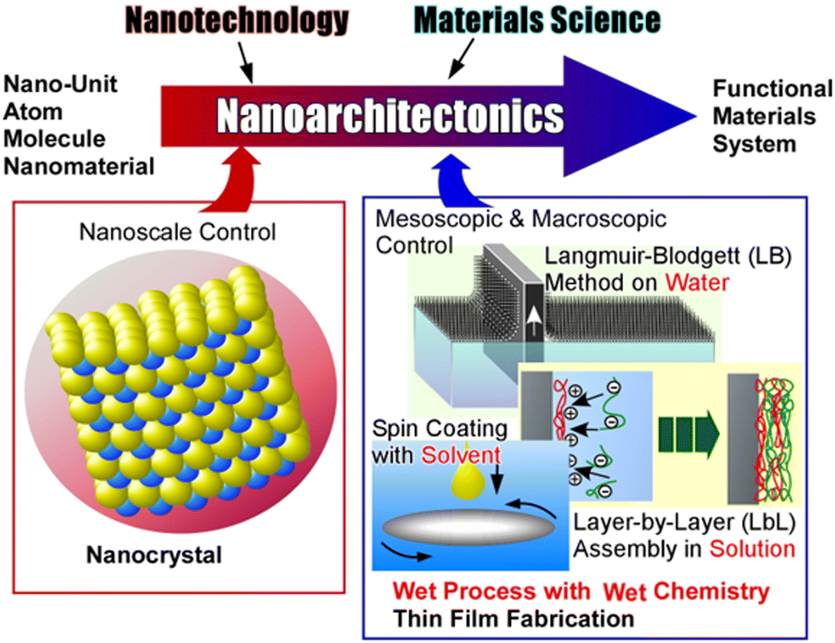
The development of these fields is distinct yet interconnected as they converge in the progression of materials development, the understanding of nanostructures, and the creation of materials with nanoscale characteristics. Just as nanotechnology has established an impactful and foundational direction for studying nanoscale phenomena, nanoarchitectonics was proposed to define a direction that integrates methods for materials development under nanoscale control. This approach will stimulate research and development more effectively than if each field were to advance independently. Nanoarchitectonics was introduced by Masakazu Aono at the start of the 21st century21 as a broad and inclusive concept for constructing functional materials from nano-units such as atoms, molecules, and nanomaterials.22 It encompasses numerous fields without imposing specific limitations on the materials used or their applications. Drawing an analogy to the super unification theory in physics, which is aiming to a theory of everything,23 nanoarchitectonics has the potential to serve as a universal methodology in materials science.24 With this perspective, it is beneficial to discuss the overview by focusing on particular examples that also encourage a reevaluation of the field.
In this review, we aim to provide the materials science and physical chemistry communities with an informed overview of recent conceptual and applicative developments in nanocrystal thin films assembled by wet chemistry nanoarchitectonics. The combination of nanocrystals, which can be deliberately structured at the nanoscale, with thin films, which hold significant promise for applications, is indeed ideal for illustrating the importance of constructing functional material systems from the nanoscale.
Nanocrystals25 are well-suited for the design, prediction, and realization of functions in small-scale structures. Because their atomic and molecular arrangements and shapes are fixed, nanocrystals possess a defined regular structure, making their functions predictable. They find wide application as optical functional materials, catalytic materials, magnetic materials, and bio-related materials. Nanocrystals often exhibit properties distinct from those of bulk crystals and amorphous materials. Indeed, at the nanoscale, the surface lattice bonds of the material are partially broken, resulting in physical properties that differ from those of solids. When crystals are formed from nanocrystals, the constituent particles must be forcibly bound together, leading to the formation of grain boundaries with disordered atomic arrangements between particles. The high proportion of these boundaries imparts unique physical properties. In addition to typical metal,26 organic molecular,27 and polymer28 nanocrystals, nanomaterials with a variety of functions are widely utilized to form nanocrystals. The materials discussed in this review include two-dimensional (2D) transition metal dichalcogenide nanosheets, plasmonic supercrystals, lead halide perovskites, organic–inorganic hybrid perovskites, zeolites, and nanocellulose, among others. Although these represent only a fraction of the many notable examples, the functions and related applications described here are already highly diverse, encompassing photonics, plasmonics, optoelectronics, electrocatalysis, sensing, storage, catalysis, separation and nanodevices. Of particular interest are the properties of chiral nanocrystals, which include chiral light absorption and emission, polarized light detectors and chiral second harmonic generation. These unique properties enable applications for enantioseparation, chiral catalysis, chiral sensing, and the control of quantum states in chiral materials under magnetic fields. Thus, chiral thin films encompassing nanocrystals are another demonstration of the value of the nanoarchitectonic approach for designing a wide range of functionalities.
Considering the above functions, the morphology of thin films is highly advantageous and their integration with functional materials such as nanocrystals is essential for device fabrication. Thin films not only benefit devices but also provide increased useful surface area and facilitate the reception of external stimuli. Although there are many dry processes for producing thin films, including the vacuum deposition of DNA and related substances,29 these assembly methods are generally challenging to apply to materials of a certain size, such as nanocrystals. In such a case, wet film formation approaches are well-suited as they allow the processing of a wide range of pre-formed nanomaterials, regardless of their composition or shape. Therefore, thin film formation of 2D nanosheets by exfoliating layered materials30 in solution and wet processes like normal adsorption,31 electrochemical deposition,32 casting,33 and spin coating34 are all commonly used. For finer control over the nanoscale films, interfacial science techniques can be used, including the self-assembled monolayer (SAM) technique,35 the Langmuir–Blodgett (LB) method,36 and the layer-by-layer (LbL) assembly.37 The latter is particularly effective for fabricating multilayer thin films of nanocrystal-like materials such as colloidal particles,38 quantum materials,39 and biological materials.40 In this review, we present research examples utilizing these and related techniques.
In this review, entitled “Wet chemistry nanoarchitectonics for nanocrystal-based films”, the fabrication of nanocrystal thin films through wet chemical processes and their resulting functional properties are explored (Fig. 1). The review is structured around three primary thin film fabrication strategies: (i) functional films assembled via adsorption of pre-formed nanocrystals, (ii) electrochemical deposition of pre-formed nanocrystals, and (iii) functional crystal films synthesized from ionic precursors. Special attention is given to the dimensionality of pre-formed nanocrystals spanning 0D, 1D and 2D, and its influence on the resulting thin films. Relevant advanced techniques are described such as layer-by-layer (LbL) assembly and liquid-surface processes akin to the Langmuir–Blodgett (LB) method, alongside applications and theoretical frameworks like graph theory for structural analysis. A dedicated section (iv) highlights pioneering advancements in chiral thin film design and functionality, enabling cutting-edge chirality-related applications. Given the vast diversity of nanocrystal targets, functions, and applications, a fully systematic organization is challenging. Instead, this review emphasizes the defining features and broader implications of wet-processed nanocrystal thin films through selected case studies. The concluding section outlines future opportunities in wet chemistry nanoarchitectonics for nanocrystal-based films, addressing scalability, multifunctionality, and integration with emerging technologies like machine learning. These themes highlight the transformative potential of nanoarchitectonics from the angle of nanoscale engineering in advancing functional thin films.
 | ||
| Fig. 1 Utilization and device integration of crystals with nanoscale control into thin films by nanoarchitectonics based on wet chemistry approaches including Langmuir–Blodgett, layer-by-layer and spin-coating. | ||
2. Thin functional films assembled by adsorption of pre-formed nanocrystals
In order to achieve precise control over nanocrystal-based functional films, it is often necessary to synthesise nano-units with the desired structural and functional features before assembling them into films, either alone or with co-deposited precursors. This approach offers a significant advantage in that it facilitates the integration of diverse chemistries and building blocks of varying shapes and sizes into thin films, utilising a limited number of processing tools. In this regard, the elaboration of films by means of adsorption processes is particularly noteworthy as it is both the most accessible and cost-effective method, encompassing techniques such as spin coating, dip coating, LbL and LB assemblies. The obtained nanostructured coatings fully embrace the realm of nanoarchitectonics, as they combine well-defined nanostructures into larger materials where both the individual and collective properties of nano-units can be harvested to offer defect-resilient functions. As the dimensionality of nanomaterials exerts a critical influence on these properties, this section introduces functional nanocrystal thin films as a function of the dimensionality of the precursors.2.1. Functional films formed from 2D crystals
Two-dimensional (2D) nanosheets, defined as single-layer structures obtained by exfoliating layered compounds, exhibit molecular-level thinness and a variety of attractive properties.41 The fabrication of nanodevices using 2D nanosheets is a highly appealing research objective that requires precise positioning of 2D nanosheets on device substrates. This is possible by using a spin-coating approach, as comprehensively demonstrated by Sakai and Sasaki (Fig. 2).42 It was demonstrated that 2D nanosheets self-assemble during the spin-coating process, leading to a surface coverage that depends on the rotation speed used (A ∝ 1/ω2). Consequently, the systematic investigation of the influence of key processing parameters (e.g. spin-coating rotation speed, nanosheet suspension concentration and substrate surface size) allowed providing guidelines for controlling the organization of 2D nanosheets on the substrate, yielding high-quality monolayer films. The method has been successfully applied to various types of nanosheets (e.g. MoS2 and Ti0.87O20.52−) and substrates, including flat and rough indium tin oxide (ITO) substrates and silicon wafers.42 Finally, a new mechanistic model was proposed for nanosheet film formation on the solvent surface rather than directly on the substrate. | ||
| Fig. 2 Spin-coating process for fabricating monolayer films of 2D nanosheets for optimising the production of high-quality monolayer films with the effects of key parameters such as the spin-coating rotation speed, the concentration of the nanosheet suspension and the size of the substrate surface. Reprinted with permission from ref. 42 copyright 2022 American Chemical Society. | ||
The controlled production of high quality 2D thin films is a key element in creating devices that exploit the full potential of 2D nanosheets. The automation of such 2D device fabrication is desirable and will facilitate high-throughput synthesis and screening. Osada and colleagues have reported a novel strategy for producing large-area, highly oriented, and densely packed 2D nanosheet films via a continuous flow-assisted assembly method (Fig. 3).43 They demonstrated the adaptability of one-drop assembly in automated fabrication utilizing a pipetting device. By carefully adjusting key control parameters (e.g. concentration, aspiration speed, and substrate temperature), dense monolayer films with high coverage (>95%) were obtained within 1–2 minutes, while ensuring the orderly arrangement of 2D nanosheets. This method enabled (i) the use of continuous flow to obtain nanosheet-oriented films, (ii) the scalable fabrication of films with controlled thickness (through multiple deposition), and (iii) generalization to different 2D materials, including Ti0.87O2, Ca2Nb3O10 and MoS2 nanosheets. These cumulated advantages positioned this method as a prime candidate for designing energy storage, electronics, and membrane technologies when compared to conventional techniques such as the Langmuir–Blodgett deposition or vacuum filtration.
 | ||
| Fig. 3 A novel approach to the fabrication of large-area, highly oriented and densely packed 2D nanosheet films using one-drop assembly: series of photographs in the film deposition process for Ti0.87O2 nanosheets (top) and plausible model for the 2D film formation mechanism (bottom). Reprinted with permission from ref. 43 copyright 2023 American Chemical Society. | ||
Despite the perspectives offered by this method for on-demand deposition and cost-effective fabrication of 2D devices, further refinement of the pipetting device will optimise the adaptability of one-drop assembly and pave the way for various 2D nanosheet applications. The same group also demonstrated a novel method for ultrafast assembly of 2D nanosheet films via spontaneous spreading on a water surface (Fig. 4).44 By employing a water/ethanol suspension containing a cationic surfactant, Marangoni-enhanced spontaneous spreading of large, uniform 2D films on the water surface was induced within 10 seconds. Both the speed and the assembly efficiency of this approach were outstanding compared to conventional adsorption techniques. In short, the exploitation of the Marangoni effect (i.e. the mass transfer along an interface between two phases caused by a gradient in surface tension) and surface tension gradients was demonstrated to drive the rapid self-assembly of 2D nanosheets with the capability for both large-scale (>4 inches) deposition and minimal material wastage. For instance, merely 10 μL of suspension sufficed to coat a 4-inch diameter surface, in stark contrast to traditional deposition methods such as spin coating (wasting more than 90% of the suspension for a single layer). Furthermore, sequential multilayer deposition enabled the on-demand production of large 2D nanofilms and freestanding films suitable for industrial-scale manufacturing. The broad applicability of Marangoni-enhanced film-assembly was demonstrated with various 2D materials, including metal oxides, graphene oxide, h-BN, MoS2, and MXene. The method's versatility was further demonstrated via the fabrication of functional films, such as transparent conductive RuO2 films exhibiting 81–96% transmittance and 100–400 Ω sq−1 sheet resistance, as well as iridescent optical films composed of high refractive index Ti0.87O2 and Ca2Nb3O10 nanosheets. This combination of optical transparency and electrical conductivity is on par with the performance of ITO electrodes, positioning RuO2 films as credible alternatives.
 | ||
| Fig. 4 A method for ultrafast assembly of 2D nanosheet films via spontaneous spreading on a water surface using a water/ethanol suspension containing a cationic surfactant (tetrabutylammonium hydroxide ion) to induce Marangoni-enhanced spontaneous spreading of large uniform 2D films on a water surface within 10 seconds: schematic illustration of spontaneous spreading of 2D nanosheets (top), series of photographs of the spontaneous spreading process (middle), and schematic illustration of the spreading behaviour of a nanosheet suspension (bottom). Reprinted with permission from ref. 44 copyright 2024 Wiley-VCH. | ||
As a versatile class of materials with well-defined porous structures, zeolites are widely used as industrial catalysts and adsorbents.45 Two-dimensional zeolite nanosheets are remarkably performant nanomaterials that cumulate a great abundance of active sites with rapid ion/molecular diffusion pathways. Using the layer-by-layer (LbL) strategy, Sasaki and colleagues46 developed hierarchical films from exfoliated unilamellar zeolite nanosheets. The alternating adsorption of cationic polymers and zeolite nanosheets produced composite multilayer films with strategic sequencing of MWW- and bifer-type zeolite nanosheets (Fig. 5). These novel hierarchical films with dual zeolite nanosheet types benefited from nanoscale precision in film thickness (2–3 nm per layer) and compositional control, resulting in engineered zeolite architectures with customized pore structures unattainable through traditional synthesis routes. Distinct hierarchical architectures were obtained through designed MWW–bifer nanosheet deposition sequences which demonstrated structure-dependent adsorption properties using rhodamine B dye as a model system. It is clear that such customized ultrathin architectures will support advanced applications in the future, including high-precision sensors, ultrathin catalytic layers, and efficient ion-exchange systems. Future functionalization potential is particularly evident when applied to MFI-type zeolites, where pore orientation perpendicular to the layers facilitates three-dimensional molecular transport.
 | ||
| Fig. 5 Fabrication strategies of hierarchical films of exfoliated unilamellar zeolite nanosheets, MWW and bifer zeolite nanosheets, using LbL assembly in different stacking orders. Reproduced under terms of the CC-BY license from ref. 46, 2024 Wiley-VCH. | ||
The multilayer and hierarchical control conferred by the LbL approach is of particular interest for reflecting electromagnetic waves, a property that is needed for mitigating electromagnetic interference (EMI). Indeed, engineering interfaces between conductive materials with markedly different impedances not only reflects electromagnetic waves but also provides strong electronic/magnetic dipoles that absorb electromagnetic waves to further reduce EMI. An additional attenuation can even be achieved by leveraging multiple internal reflections in the films, which occur due to scattering structures or defects within the shielding material itself. A notable approach to EMI shielding was reported by Kim and co-workers, who developed hierarchical porous copper films using a cost-effective LbL assembly of 2D copper nanosheets (Fig. 6).47 Large single-crystalline copper nanosheets were vertically stacked, resulting in the simultaneous formation of multilayered 2D structures and sheet-like cavities enabling the combination of copper's high electrical conductivity with a tailored porous architecture to enhance shielding effectiveness. The resulting films showed exceptional EMI shielding effectiveness, reaching 100 dB for a thickness of just 15 μm with a high specific shielding effectiveness of 292![[thin space (1/6-em)]](https://www.rsc.org/images/entities/char_2009.gif) 000 dB cm2 g−1 at 1.6 μm thickness. In comparison, commercial EMI shielding typically achieved lower efficiency (<80 dB) for thicker films (>100 μm). The shielding effectiveness was retained over 24 months under ambient conditions, while around 80 dB was still achieved after annealing at 200 °C for one hour. In addition, the film exhibited mechanical flexibility, maintaining performance after 5000 bending cycles. LbL-produced porous copper films are thus strong candidates for integration into next-generation commercial shielding barriers, demonstrating how the film-integration of 2D metallic nanocrystals can enable practical advancement across a broad spectrum of electronic applications.
000 dB cm2 g−1 at 1.6 μm thickness. In comparison, commercial EMI shielding typically achieved lower efficiency (<80 dB) for thicker films (>100 μm). The shielding effectiveness was retained over 24 months under ambient conditions, while around 80 dB was still achieved after annealing at 200 °C for one hour. In addition, the film exhibited mechanical flexibility, maintaining performance after 5000 bending cycles. LbL-produced porous copper films are thus strong candidates for integration into next-generation commercial shielding barriers, demonstrating how the film-integration of 2D metallic nanocrystals can enable practical advancement across a broad spectrum of electronic applications.
 | ||
| Fig. 6 Hierarchical porous copper films fabricated by LbL assembly for electromagnetic interference shielding, where large sheets are vertically stacked to simultaneously create multi-layered 2D structures and sheet-like cavities: actual morphology (left) and model (right). Reprinted with permission from ref. 47 copyright 2021 American Chemical Society. | ||
2.2. Functional films formed from 1D crystals
While non-stabilized 2D nanocrystals have a natural tendency towards stacking in solution, which is beneficial for designing films, the planar orientation of 1D nanocrystal assemblies is more challenging. Nevertheless, this reduced dimensionality also provides opportunities for new functions to emerge, such as chiral films and complex entangled nanostructured coatings.Chirality arises from spontaneous symmetry breaking and is considered a fascinating scientific phenomenon with profound implications across all length scales.48 Hierarchical nanocrystal assemblies are particularly valuable for investigating how chirality can be amplified through symmetry breaking, as they allow for the study of chirality transfer across multiple size regimes. Hanrath and co-workers have carried out comprehensive research on the emergence and reversal of chirality in hierarchical assemblies of CdS nanocrystal fibers.49 The ability to precisely control the hierarchical structure of fiber arrays was identified as a key direction for future research and represents a significant advancement toward the programmable formation of chiroptical metamaterials. Hierarchical nanocrystal assemblies were formed with CdS nanocrystals arranged in bands of approximately 2 μm, and these structures were uniform across over 2 cm scale films. An unusual observation of opposite chirality was made between the top and bottom surfaces of the films. The relationships between the process, structure, and properties in these systems were clarified by systematic investigation of the geometrical arrangement of CdS nanocrystals in hierarchical assemblies and its effect on the chiroptical properties. Consequently, a novel mechanism for chirality inversion was proposed, based on the interplay of hydrodynamic and physicochemical processes. These findings highlight the importance of the mesoscale structure in determining chiroptical properties, particularly with respect to variations in fiber orientation and undulation amplitude. Therefore, the development of more complex, macroscopically patterned chiroptical films will need to consider design principles such as the control of local hydrodynamic conditions. Indeed, by modifying the substrate and designing patterns with specific local contact angles, it is possible to manipulate local hydrodynamic shear and thereby design and fabricate chiroptical metamaterials with improved structural characteristics. The hierarchical structure of fibre arrays is thus an exciting step towards the programmable formation of chiroptical metamaterials with potential applications in sensing, hyperspectral imaging, and quantum information technology.
The development of breakthrough materials necessitates the simultaneous consideration and optimization of multiple properties, including electrical, mechanical, thermal, and optical characteristics. Achieving such multidimensional optimization is inherently challenging and often requires empirical iteration of assembly techniques. Computational models may serve as critical tools for accurately predicting the interdependent properties of complex structures, enabling concurrent calculations of mechanical deformation, charge transport, and optical absorption. Glotzer, Goss, Kotov, and collaborators have introduced a novel approach for designing and analyzing multifunctional nanostructured coatings through the integration of LbL assembly and graph theory (Fig. 7).50 Their work demonstrated that graph theory can effectively describe the structural and functional characteristics of LbL composites comprising Ag and Au nanowires. A predictive framework for complex nanostructured materials was established via the direct use of microscopy images to inform graph theoretical models and the description and prediction of anisotropic properties in aligned nanowire films. For instance, sheet resistance in multilayer films and correlated bond percolation thresholds with current-carrying capacity were accurately predicted. Prediction of conductivity anisotropy in aligned nanowire films was also realised and scalability was demonstrated. Therefore, graph theory parameters provided practical structural descriptors for composites incorporating diverse rod-like nanoscale components and offered a benchmark for enhancing machine learning interpretability. This feature is often absent in conventional image analysis algorithms. Furthermore, the non-linear and non-reciprocal effects of seemingly simple parameters expanded the applicability of machine learning tools for property prediction in such systems.
 | ||
| Fig. 7 An approach to the design and analysis of multifunctional nanostructured coatings using LbL assembly and graph theory, which provides a framework for predicting and tuning multiple properties simultaneously: schematic of 2D confinement of adsorbed nanowires (top) and actual image and graph theory models for LbL assemblies of Ag nanowires and Au nanowires (bottom). Reprinted with permission from ref. 50 copyright 2025 Elsevier. | ||
Combining 1D nanocrystals with grazing incidence spraying and LbL assembly allowed the development of nanostructures exhibiting strong and spectrally tunable circular dichroism (CD) bands (Fig. 8).51 In such coatings, interparticle interactions and plasmonic coupling critically influence the chirality and associated chiroptical properties of surfaces. This unique property makes them highly valuable for chiral sensing applications involving molecules with weak intrinsic chiroptical signals and absorption bands in the UV-visible range. This approach enabled precise control over mesostructural features, such as nanoscale spacing between plasmonic layers and the angular orientation of Ag nanowire layers, facilitating tailored chiroptical responses with exceptionally high CD values across broad spectral ranges. The structure-dependent optical properties were effectively modeled using a transfer matrix formalism, establishing straightforward design principles for engineering chiral plasmonic metasurfaces with targeted functionalities. Distinctive advantages of this method included (i) fine mesostructural control for tuning chiroptical properties, (ii) scalable fabrication using commercially available materials, and (iii) independent modulation of CD intensity (via angle α) and spectral profiles (via interlayer spacing d). The CD activity was directly governed by structural parameters: increasing interlayer spacing induced the redshift of CD peaks in the visible/NIR region, while interference effects at larger spacings (>100 nm) produced oscillations in the CD spectra. The scalability of this technique was demonstrated through large-area fabrication on 12′′ × 12′′ substrates. Therefore, such chiral plasmonic metasurfaces hold promise for polarization-sensitive photodetectors, chiral second harmonic generation, enantioseparation via chiral optical forces, and catalytic or sensing applications.
 | ||
| Fig. 8 A method to fabricate chiral plasmonic nanostructures with highly tuneable chiroptical properties using a combination of grazing incidence spraying and LbL assembly. Reprinted with permission from ref. 51 copyright 2021 American Chemical Society. | ||
Decher, Pauly et al. have extended the same approach to the fabrication of large-area, highly ordered nanoparticle superlattice films to create chiral Bouligand-type assemblies. Bouligand structures are hierarchical structures composed of multiple layers of aligned fibers, with each layer rotated at a fixed angle relative to the previous one. This resulted in functional films with twisted morphologies, providing an efficient route for producing large-area chiral plasmonic metasurfaces (Fig. 9).52 A key advantage of these architectures is that chirality can emerge solely from the spatial geometric arrangement, even when the fundamental building blocks (1D objects) themselves are achiral. Such structures are found in nature and are responsible for remarkable mechanical properties, as exemplified by the phalanx of the mantis shrimp. Artificial fabrication of Bouligand structures is also possible through methods such as nanolithography, which can result in pronounced circular dichroism. Combining 1D nanocrystals with grazing incidence spraying and LbL assembly allowed tuning the nanoscale pitch direction, including left- or right-handed orientation, by simple rotation of the sample during the spray deposition of individual nanorod or nanowire layers. Consequently, highly ordered superlattice films with domain sizes exceeding 50 μm2 were obtained onto various substrates with helical anisotropy and long-range orientational order with correlation lengths up to 1 mm. This methodology confers significant benefits in scalability, long-range order, and versatility, enabling the production of highly ordered nanoparticle superlattice films and allowing for precise tuning of optical properties through control of interparticle spacing and superlattice architecture properties. This method for long-range structural ordering was applied to a broad spectrum of nanoparticle types and sizes (e.g. Au, Ag, Fe3O4, and PbS with sizes ranging from 5 to 20 nm), providing a promising strategy for the template-free fabrication of chiral structures with nanoscale structural tuning. Ultimately, this facilitates the design of advanced multi-material nanocomposites with complex anisotropic characteristics.
 | ||
| Fig. 9 Fabrication of chiral Bouligand-type LbL assemblies by oblique incidence spraying with controlled directions and angles, which is an efficient approach to fabricate large-area chiral plasmonic metasurfaces. Reprinted with permission from ref. 52 copyright 2021 American Chemical Society. | ||
1D nanocrystal-based chiral films with circularly polarised luminescence were also obtained via the Langmuir–Schaeffer technique. These materials attracted considerable attention due to their potential applications in three-dimensional optical displays, bio-encoding, asymmetric catalysis and photovoltaic devices. Ma, Kuang and co-workers have successfully fabricated chiral light-emitting films with robust and highly tuneable chiroptical activity properties using CdSe/CdS semiconductor nanorods (Fig. 10).53 In this work, semiconductor nanorods (used as an alternative to conventional metal nanoparticles) were integrated in the films with precise structural control by modulating the number of deposited layers and the interlayer angular orientation. Large-scale fabrication (>4 inches) of uniform chiral films was achieved, complemented by electromagnetic simulations that validated the chiral characteristics of the assembled architectures. Leveraging the intrinsic luminescence of CdSe/CdS nanorods, the resulting chiral films exhibited both pronounced chiral activity and substantial circularly polarized luminescence (CPL) signals, broadening the functional scope of circularly polarized luminescence devices in practical applications.
 | ||
| Fig. 10 Fabrication of chiral plasmonic nanostructures with highly tuneable chiroptical properties using CdSe/CdS semiconductor nanorods by the Langmuir–Schaeffer method. Reprinted with permission from ref. 53 copyright 2021 Wiley-VCH. | ||
2.3. Functional films formed from 0D crystals
While 2D and 1D nanocrystals promote the formation of stacked or entangled networks inside thin films, large-scale structural order in 0D nanocrystal films, which relies on their good packing, is not easily achieved. In fact, thin film integration of 0D nanocrystals is by far the most investigated case in the context of adsorption-based wet-chemistry assembly of nanocrystal films. Achieving structural control of these films has been the focal point of recent investigations, with the aim of rationalizing their structure–composition–property relationship.The self-assembly of cellulose nanocrystals into structurally colored films is of particular interest due to the potential for developing more sustainable photonic pigments. Vignolini and colleagues achieved large-scale production of structurally colored cellulose nanocrystal films through roll-to-roll deposition (Fig. 11).54 This industrially relevant process was achieved by casting cellulose nanocrystal suspensions using commercially available coating equipment. The approach provides a scalable and industrially viable method for producing sustainable, structurally colored materials, marking the first demonstration of meter-long films created with commercial roll-to-roll deposition tools. Optimizing the coating parameters that govern self-assembly enabled tunable structural colors spanning the visible spectrum, a versatility that was further demonstrated through solvent-induced swelling. At the same time, the films exhibited a remarkable stability, with unchanged structural color even after immersion in water for more than 1.5 years, an outstanding performance as compared to sustainable organic pigments. These advances demonstrate the promise of photonic pigments as environmentally friendly alternatives to traditional materials for industrial applications, such as replacing non-biodegradable microplastic glitter in paints and packaging.
 | ||
| Fig. 11 Large-scale production of structurally coloured cellulose nanocrystal films using roll-to-roll deposition: flow chart (top), process photos (middle), and schematic of the pathway (bottom). Reprinted with permission from ref. 54 copyright 2021 Springer-Nature. | ||
Well-controlled assemblies of 0D nanocrystals are also of interest for enhanced vibrational spectroscopy. Plasmonic supercrystals are highly ordered, three-dimensional assemblies of plasmonic nanoparticles, in which light is tightly confined to regularly spaced electric field hotspots. This configuration significantly enhances the light–matter interactions of molecules embedded within the supercrystal. The high density of these hotspots is especially beneficial for vibrational spectroscopy, as their small cross-sectional area leads to pronounced signal enhancement. Mueller et al. fabricated plasmonic supercrystals that serve as effective platforms for surface-enhanced vibrational spectroscopy, delivering reproducible and uniform signal enhancement.55 Gold nanoparticle supercrystals were synthesized via self-assembly on a liquid subphase, with polystyrene molecules acting as spacers between nanoparticles. Reproducible and tunable surface-enhanced spectroscopy was achieved by correlating the structural and optical properties of these supercrystals. Surface-enhanced Raman scattering (SERS) resonances, resulting from the overlap of incoming and outgoing polariton modes, were observed, and a coupled oscillator model was employed to explain the enhancement observed in surface-enhanced infrared absorption spectroscopy (SEIRAS). The peak integrated SERS enhancement reached up to 300, with individual hotspot enhancements as high as 105 which can be considered a high performance. Additionally, SEIRAS enhancement increased by up to 400% when the polariton resonance was matched to the molecular vibrational frequency. Furthermore, plasmonic supercrystals composed of multiple nanoparticle layers were capable of supporting several polariton resonances across the mid-infrared to near-infrared spectral range, enabling the integration of polariton-mediated SERS and SEIRAS on a single substrate.
Confinement at the nano- or microscale, particularly within geometrically defined pores, exerts a pronounced influence on crystallization processes. The fabrication of structures within lithographically engineered groove patterns on substrates enables the production of devices featuring sub-wavelength dimensions and precisely controlled morphological characteristics. Lee, Mirkin et al. demonstrated the assembly of DNA-functionalized gold nanocubes under microscale lateral confinement (Fig. 12)56 by fabricating square trenches on DNA-functionalized substrates using electron beam lithography (EBL). This approach leveraged EBL to create geometrically defined confinement environments, enabling precise control over superlattice formation. The DNA-functionalized substrate facilitated programmable interactions, while the square trench morphology guided the nanocubes into ordered configurations through spatially restricted self-assembly pathways. Control over the superlattice size, orientation and defect structure was achieved through microscale confinement. The superlattices formed square prism shapes filling the entire trench volume while smaller trenches (1 μm) produced higher quality assemblies with fewer defects.
 | ||
| Fig. 12 Assembly of DNA-functionalised gold nanocubes under lateral confinement in microscale square trenches on a DNA-functionalised substrate using electron beam lithography to pattern the square: trench array fabrication process (top), superlattice assembly scheme (middle), and SEM images of representative superlattices grown in 3, 2, and 1 μm trenches (bottom). Reprinted with permission from ref. 56 copyright 2022 American Chemical Society. | ||
Natural materials serve as significant inspiration for designing artificial photonic systems and multifunctional devices. For instance, films incorporating helical arrays of cellulose nanocrystals exhibited remarkable photonic properties and structural anisotropy. As shown in Fig. 13, Zhang, Qing, Liu et al. have developed a simple and robust method to co-assemble cellulose nanocrystals with poly(ethylene glycol)dimethacrylate (PEGDMA) monomers in N,N-dimethylformamide.57 Solvent resistant, chiral nematic and vivid iridescent composites were obtained by UV induced free radical polymerisation. Through UV-initiated free radical polymerization, solvent-resistant, chiral nematic composites with vivid iridescence and mechanochromic properties were obtained. Under mechanical strain, the material exhibited mechanochromism, transitioning from red to green as strain increased. Moisture exposure triggered rapid bending (4.6° s−1) and complex 3D deformations, mimicking natural tendril coiling. Intriguingly, the actuation favored right-handed helical configurations with a 63% probability, reflecting the intrinsic left-handed chirality of the CNC template. These properties established a foundation for bioinspired photonic materials capable of dual optical and mechanical responsiveness.
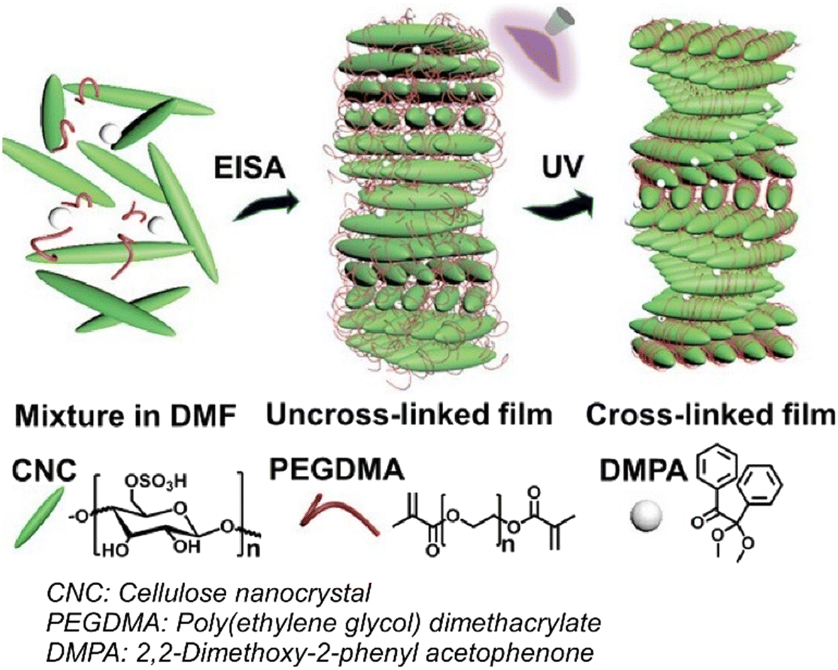 | ||
| Fig. 13 A simple and robust method to co-assemble cellulose nanocrystals with poly(ethylene glycol)dimethacrylate (PEGDMA) monomers in N,N-dimethylformamide by integration of cellulose nanocrystal self-assembly with UV-initiated polymerisation. Reprinted with permission from ref. 57 copyright 2022 Wiley-VCH. | ||
Lead halide perovskite nanocrystals are highly regarded for their exceptional photoluminescence quantum yields, tunable emission across broad spectral ranges, and cost-effective solution processability, positioning them as promising candidates for next-generation light-emitting diodes (LEDs). Extensive research has focused on enhancing their performance through compositional engineering strategies such as doping, alloying, surface passivation, morphology optimization, and interface engineering. These advancements have elevated the external quantum efficiency (EQE) of perovskite nanocrystal LEDs to about 20%, marking significant progress toward practical applications. Yao and colleagues demonstrated the fabrication of high-performance green perovskite nanocrystal light-emitting diodes using weakly confined CsPbBr3 nanocrystals with a diameter of 18 nm, which exhibited the highest colour purity, high external quantum efficiencies and good operational stability (Fig. 14).58 The film formation was based on the innovative use of a calcium tributylphosphine oxide (Ca-TBPO) passivation strategy that enhanced colloidal stability and film uniformity, and the exploitation of large nanocrystal dimensions to mitigate non-radiative recombination. A narrow emission linewidth was obtained, which ensured high color purity and a rapid brightness increase near the turn-on voltage, indicative of efficient charge injection. Thus, large perovskite nanocrystal films offered an original pathway to balance optical performance, efficiency, and device longevity. Further developments of perovskite-based films for LEDs will support applications in displays, solid-state lighting, and optoelectronics requiring precise color control and robust operation.
 | ||
| Fig. 14 Fabrication of perovskite nanocrystal light-emitting diodes using weakly confined CsPbBr3 perovskite nanocrystals with a diameter of 18 nm, which exhibit the highest colour purity, high external quantum efficiencies and good operational stability: SEM image (right top) and assembly model (right bottom). Reprinted with permission from ref. 58 copyright 2021 American Chemical Society. | ||
In summary, nanocrystals of varying dimensionalities have enabled the synthesis of functional thin films with tailored properties, driven by the structure–property–processing relationship of the assembled materials. Two-dimensional nanosheets typically produce highly oriented films with tuneable thickness that are desirable for energy storage applications and for electromagnetic interference shielding. One-dimensional nanocrystal assemblies, such as CdS fibers, leverage mesoscale chirality to achieve programmable optical metamaterials for sensing. Zero-dimensional nanocrystals, like cellulose nanocrystals, enable scalable production of structurally coloured films with tuneable optical responses while large-sized lead halide perovskite nanocrystals demonstrate high-efficiency LEDs. The selection of the dimensionalities of pre-engineered nanocrystals in accordance with target properties is thus of critical importance in the design of functional thin films.
3. Thin functional films assembled by electrochemical deposition of pre-formed nanocrystals
Electrochemical film assembly methods using pre-formed functional nano-units stand out due to their capability to direct the growth of conformal films with well controlled thicknesses. In this regard, the electrochemical stimulus aims to either induce precipitation of well-suspended precursors (e.g. electrodeposition, performed with the precursor alone or by co-precipitation) or induce their reticulation on the electrode surface (e.g. electrosynthesis).59 In both cases, the surface-confined nature of the electrochemical stimulus is key to controlling the spatial deposition, homogeneity and thickness of the films. Here, two prominent methods are reviewed: electrophoretic deposition and electrosynthesis of films from pre-engineered nanocrystals.Robust, low-cost, and highly transparent functional nanocomposite thin films have garnered significant attention due to their potential in energy-saving technologies. These materials hold promise for applications such as light/color management devices, photovoltaic luminescent solar concentrators, and smart solar-control windows. Grasset, Uchikoshi et al. have developed three distinct types of transparent 0D metal cluster/polymethyl methacrylate (PMMA) nanocomposite films fabricated via electrophoretic deposition (EPD) on indium tin oxide (ITO)-coated glass substrates (Fig. 15).60 Dual UV-NIR blocking and red-NIR luminescence properties were obtained with transparent nanocomposite films combining octahedral Mo6 and Nb6 metal clusters with PMMA, demonstrating their utility for optical applications. Homogeneous films with thicknesses of up to 1.5 μm were achieved, featuring high cluster loadings (29 wt% for Mo6 and 6 wt% for Nb6 clusters). Mo6@PMMA films maintained excellent photoluminescence quantum yields even after 4 weeks of exposure to 50 °C and 70% relative humidity, underscoring their environmental stability. These materials are thus promising candidates for energy-efficient optical windows, where simultaneous light management and durability are critical.
 | ||
| Fig. 15 Fabrication of highly transparent metal cluster/PMMA nanocomposite thin films on indium tin oxide-coated glass by electrophoretic deposition. Reproduced under terms of the CC-BY license from ref. 60, 2019 The Royal Society of Chemistry. | ||
EPD was also used for film integration of 2D nanocrystals such as MoS2 nanosheets. Indeed, 2D transition metal dichalcogenides are being studied intensively to find earth-abundant and low-cost alternatives for the development of optoelectronic devices. Optoelectronic devices based on 2D transition metal dichalcogenides have high optical absorption coefficients over a wide spectral range, allowing them to be used for the detection of very weak optical signals. Bhakhar, Pataniya, Solanki et al. have fabricated photoelectrochemical photodetectors embedding MoS2 nanosheets by EPD (Fig. 16).61 The electrodeposition of liquid-phase exfoliated MoS2 nanosheets resulted in thin films (of 59 nm maximum) with a vertical alignment of the nanosheets. This vertical orientation was particularly advantageous because the ab-basal planes of MoS2, which are inactive for electrochemical charge transport, were positioned perpendicular to the substrate. As a result, the surface-to-volume ratio of the films was significantly increased compared to flat-lying nanosheets, enhancing electrochemical charge transport and overall device performance. The resulting electrodes demonstrated a photocurrent density of 0.5 μA cm−2 at zero bias under illumination with 670 nm light at an intensity of 100 mW cm−2. While this sensitivity performance is moderate, the photodetector exhibited fast response characteristics, with both rise and decay times measured at 0.3 seconds, indicating rapid and efficient photodetection.
 | ||
| Fig. 16 Fabricated photoelectrochemical photodetectors using electrophoretically deposited MoS2 nanosheets, in which liquid-phase exfoliated MoS2 nanosheets were deposited on conductive substrates by electrophoretic deposition: deposition scheme (top) and images (bottom). Reprinted with permission from ref. 61 copyright 2022 Elsevier. | ||
Building on the same system, electrodes for hydrogen production by electrochemical water splitting were investigated. In such a case, the hydrogen evolution reaction (HER) plays an important role for hydrogen production.62 The development of high-performance precious and non-precious metal-based electrocatalysts is a key effort to facilitate the development of this technology. Pataniya et al. reported that the electrocatalytic HER performance of MoSe2 nanosheets can be significantly enhanced by combining liquid phase exfoliation, partial oxidation and EPD.63 The electrocatalytic activity of MoSe2 nanosheet films for the HER was improved by increasing the concentration of catalytically active sites, by reducing charge transfer resistance, by forming an oxygen-deficient MoOx phase, and by utilizing photogenerated charge injection.
The binder-free MoSe2–MoOx electrodes were prepared by EPD onto silver foil and benefited from a larger surface-to-volume ratio compared to bulk nanosheets. Under 670 nm illumination, the electrodes achieved a high photoresponsivity of 0.34 A W−1 and an external quantum efficiency of 62.9%, both excellent performances for solution-processed films. In addition to high activity, the electrodes demonstrated excellent operational stability, maintaining performance over 60000 seconds and showing minimal overpotential change after 1000 cycles of cyclic voltammetry. Film integration of 2D nanocrystals by EPD stands thus as a promising approach for solar-assisted electrocatalysts, advancing clean hydrogen production technologies.
Electrosynthesis approaches were also employed for nanocrystal film assembly. While optically confining materials using highly dispersed nano-objects in covalently bonded thin films have been widely investigated to minimise pathological effects on the eye and damage to optical sensors, this approach is at a disadvantage in terms of practical applications due to the good transparency of thin films. Li, Chen and co-workers demonstrated the tuning of optical confinement properties using heterosized gold nanoparticles and electrosynthetically assembled fullerenes.64 Gold nanoparticles and C70, which have different optical limiting mechanisms, free carrier absorption and reverse saturable absorption, were electrochemically integrated into the same film by exploiting the C–C coupling reaction of carbazole with pyrene functions by cyclic voltammetry. The synergistic interplay between Au NPs and C70 was explored, focusing on their combined influence on nanostructure dimensions and optical confinement performance. Films incorporating heterosized Au NPs and C70 merged the free carrier absorption of Au NPs with the reverse saturable absorption of C70. It was shown that multilayered heterosized Au NP films with periodic bilayer architectures exhibit superior optical limiting compared to monosized Au NP films. Meanwhile, the reverse saturable absorption of C70 contributed more significantly to optical confinement than the free carrier absorption of Au NPs in hybrid films. Therefore, hybrid nanostructures based on reverse saturable absorption may be a great potential strategy for programmable electrochemically fabricated high performance optical confinement films.
Leveraging on a different electrosynthesis approach, covalently reticulated nanoparticle thin films were also proposed in the context of lateral confinement. Pichon, Boulmedais and co-workers reported an electro-click approach for the specific surface integration of gold and iron oxide nanoparticles by covalent bonding into nanodevices, with potential applications in biosensing and granular electronics (Fig. 17).65 A high aspect ratio nanodevice consisting of two gold electrodes separated by a 40 μm long, 100 nm wide nanotrench was utilized to induce the covalent self-assembly of nanoparticle films selectively in the nanotrench. This methodology established a robust platform for fabricating functional nanoparticle films with precise spatial control and enhanced interparticle coupling. The originality of this approach relied on its one-pot electroclick self-construction strategy where dendronized iron oxide nanoparticles functionalized with azide and alkyne groups served as modular building blocks. Spatially restricted electroclick reticulation was achieved through localized electrochemical generation of Cu(I) catalysts. A linear film growth rate of 0.28 nm min−1 was obtained, permitting fine thickness modulation. Non-linear current–voltage curves in nanoparticle-filled nanotrenches were obtained, indicative of Coulomb blockade behavior and offering potential applications in granular electronics. The versatility of this method stems from its reliance on functionalized commodity nanoparticles, which can be extended to diverse nanoparticle types bearing clickable moieties. By combining programmable electrochemical control with modular nanomaterial design, the approach bridges nanoscale assembly principles with macroscale device fabrication.
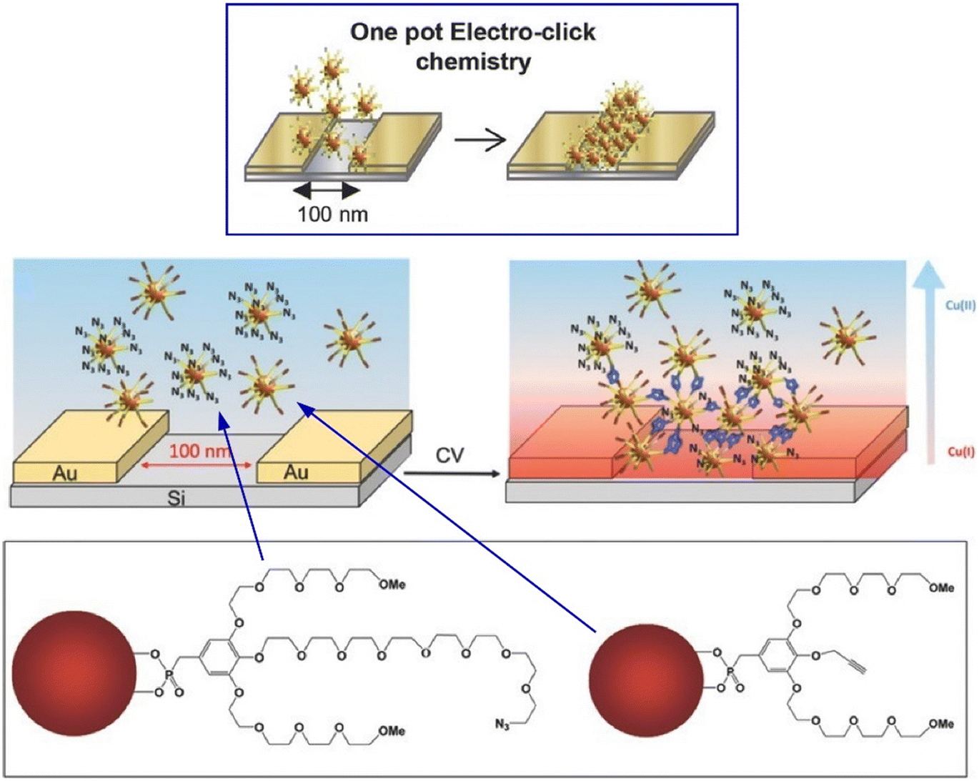 | ||
| Fig. 17 An electro-click approach for the specific surface integration of gold and iron oxide nanoparticles by covalent bonding into nanodevices to selectively fill the nanotrench. Reprinted with permission from ref. 65 copyright 2015 Wiley-VCH. | ||
Two major challenges were the focal points of building devices with nanomaterials: achieving one-pot deposition of films and controlling structures at the nanoscale. For example, films containing nanocapsules have attracted attention to enable the development of biomaterials, sensors and energy storage devices while this morphology allows accommodating the large volume changes associated with electrochemical cycling in energy storage devices. Sciortino, Rydzek et al. demonstrated the electroclick approach to create multifunctional nanocapsule coatings with controlled release capabilities (Fig. 18).66 The assembly of hybrid films was achieved using a one-pot electro-click approach, where hybridosomes (hybrid nanocapsules functionalized with polyacrylic acid bearing alkyne groups) were crosslinked with homobifunctional polyethylene glycol linkers containing azide functionalities. This process took place on a fluorine-doped tin oxide (FTO) electrode and was driven by the electrochemical generation of Cu(I) ions, which catalyzed the alkyne–azide cycloaddition reaction between the hybridosomes and the PEG linkers. This method effectively combined the unique properties of nanocapsule-based materials with the spatial precision offered by electrochemical techniques, enabling the construction of hybrid films from pre-formed hybridosomes in a single step. Furthermore, these electro-clicked films exhibited stimuli-responsive behavior: the encapsulated contents within the nanocapsules could be rapidly released in response to either a drop in pH or electrochemical oxidation. Upon activation by these triggers, the films disintegrated, releasing more than 95% of their cargo within 15 minutes. This work opened up the prospects of multifunctional films with desired chemical diversity, controllable stability and hollow nanostructures for the design of even more complex physicochemical interfaces.
 | ||
| Fig. 18 Electroclick approach to create multifunctional coatings with controlled release capabilities, where hybridosomes with functional polyacrylic acid-bearing alkyne moieties were reticulated by electroclick reaction with azide-bearing homobifunctional polyethylene glycol linkers on an F–SnO2 (FTO) electrode. Reprinted with permission from ref. 66 copyright 2018 The Royal Society of Chemistry. | ||
To sum-up, electrochemical approaches are highly suitable for assembling functional thin films due to their precise control, scalability, and environmental benefits (e.g. low energy cost and limited solvent use). Both electro-active and electro-inert (nano)crystals can be incorporated into the films using one-pot electrophoretic deposition and electrosynthesis. Interactions between the nano-units and other film components can be tuned from adsorption to covalent bonding using crystal-surface chemistry, while the film morphology, thickness and specific deposition can be adjusted by electrochemical parameters. Electrochemical approaches for film assembly from pre-formed nanocrystals are especially well-suited to assembling hybrid organic/inorganic thin films, which opens perspectives for synergetic combination of their respective properties.
4. Thin functional crystal films assembled from ionic precursors
The direct synthesis of crystals within thin films offers distinct advantages over conventional nano-crystal deposition approaches, as it circumvents the necessity for synthetic steps and the characterisation of precursors. In such cases, the conversion of ionic precursors into (nano)crystals within the films is affected by thermal, electrochemical or photochemical stimuli. Metal ions are particularly well-suited to this process due to their solubility in polar solvents and their ability to undergo reduction or oxidation into (nano)crystals in response to physico-chemical stimuli. The combination of these features with self-assembled nano-units (e.g. surfactants, copolymers) or pre-engineered matrices (e.g. mesoporous substrates) gives access to specific structural control over the functional films.Mesoporous metal oxides have always been of interest as materials for clean energy generation and storage.67 They have been investigated as electrode materials in lithium-ion batteries, supercapacitors, electrocatalysts for water oxidation, fuel cells, etc. Their critical parameter criteria for designing advanced electrode materials include stability, ease of fabrication, and the utilization of earth-abundant elements. The work by Dag and collaborators underscores the significance of mesoporous metal oxide thin films with enhanced electrochemical properties for advancing energy storage and conversion technologies.68 These mesoporous oxides, particularly when employed as electrocatalysts for water oxidation and related processes, depend critically on structural parameters (e.g. porosity and pore size). Mesoporous and pure-phase CaFe2O4 thin films were synthesized using salt-surfactant lyotropic liquid crystal templates and 800 °C annealing, yielding ordered pore structures with high surface areas (up to 74 m2 g−1). The film thickness was modulated by diluting the precursor solution, while the porosity and pore size were tailored via annealing temperature adjustments. The films deposited on electrodes exhibited exceptional electrochemical performance: a specific capacitance of 509 F g−1 at 5 mV s−1, a rate capability of 328 F g−1 at 100 mV s−1, and 95% capacitance retention after 5000 cycles. Notably, the oxygen evolution reaction (OER) was found to occur predominantly at the electrode's outermost surface, emphasizing the importance of surface morphology over bulk porosity in electrocatalytic water oxidation. This insight redirects focus toward surface engineering rather than solely maximizing internal porosity. Further investigation into solvent effects and electrode thickness for other mesoporous metal oxides is necessary to elucidate fundamental principles of mesoporous thin films for electrocatalyst design.
Organic–inorganic hybrid perovskites have electronic and optoelectronic properties that make them attractive for many device applications.69 In particular, single crystal hybrid perovskites have improved carrier transport and stability compared to their polycrystalline counterparts due to their orientation dependent transport behaviour and low defect concentration. However, single-crystal hybrid perovskites have the disadvantage that they are difficult to prepare with well-controlled morphology and composition. Xu et al. introduced a solution-based lithography-assisted epitaxial-growth-and-transfer technique for fabricating flexible single-crystal perovskite devices (Fig. 19).70 This approach enabled the production of high-quality, flexible single-crystal perovskite films with enhanced performance and stability relative to conventional polycrystalline counterparts. The devices have shown a certain mechanical flexibility with bending radii up to 2.5 mm for 2 μm thick films. By incorporating lead–tin gradient alloying, bandgap-graded single-crystal perovskites were synthesized, facilitating improved carrier mobility and reduced recombination. Solar cells utilizing these graded structures achieved an average power conversion efficiency of 18.77% which is excellent for flexible devices although higher efficiency can be reached for rigid devices.70
 | ||
| Fig. 19 An approach to flexible single-crystal perovskite devices assembled using a solution-based lithography-assisted epitaxial growth and transfer technique providing high-quality, flexible single-crystal perovskite devices with improved performance and stability: schematics of the process (left) and images (right). Reprinted with permission from ref. 70 copyright 2020 Springer-Nature. | ||
Electrodeposition approaches can also be used for the formation of nanocrystals in situ within thin films. Surface incorporation of noble metal nanostructures with controlled size and distribution is an attractive platform for applications in catalysis, sensing, optics, energy and biomedical devices, as they exhibit different physical–chemical properties from their bulk counterparts. Nasir, Hector and co-workers demonstrated the electrodeposition of nanostructured gold using mesoporous silica thin films as hard templates.71 First, films with three-dimensional mesopore structures were created by using either the evaporation-induced self-assembly (EISA) or the electrochemically assisted self-assembly (EASA) procedures. Then gold was electrodeposited in the mesopores, starting from ionic precursors. Using this approach, the size of the nanoparticles can be somehow determined from the pore size of the template (typically below 10 nm). In the future, it may be possible to increase the robustness of mesoporous silica films by reducing the microporosity and increasing the density of the silica walls. This would promote uniform pore filling and nanostructure growth within the mesopores, rather than growth beyond the pore walls.
Another electrodeposition strategy was developed to assemble nanocrystal-based battery-supercapacitor hybrid systems starting from ionic precursors. Ambare et al. employed a straightforward, cost-effective electrodeposition process to synthesize binder-free Bi2CuO4 nanostructures directly on copper substrates, with deposition time as a key variable.72 The vertically aligned Bi2CuO4 nanosheets, resembling spruce leaf-like morphologies, enhanced the surface-to-volume ratio and facilitated efficient electrochemical charge transport. Optimized electrodes achieved a specific capacitance of 706.47 F g−1 at a scan rate of 2 mV s−1, a value largely exceeding the capacitance of commercial supercapacitors, attributed to the high surface area and structural advantages of the nanosheets. Asymmetric solid-state devices incorporating Bi2CuO4 as the anode electrode demonstrated practical utility, leveraging the material's high energy density and redox capability. These devices exhibited exceptional cycling stability, retaining 98.15% of their initial capacity after 5000 charge–discharge cycles.
In summary, the stimuli-driven synthesis of nano-crystals within thin films allows for precise control over nanocrystal growth, with direct benefits for energy, catalysis, and optoelectronic applications. The exact crystal phase can be adjusted using thermal and/or electrochemical annealing while the nanostructure is adjusted using structure directing agents. In this regard, soft mesophases (liquid crystals and surfactant assemblies) and hard templates (mesoporous substrates) are prime additives to provide well controlled nanostructures, but this strategy requires a template elimination step. In contrast, this drawback is circumvented by lithographic epitaxy methods.
5. Thin functional crystal films for chiral applications
The combination of structural control and (nano)crystal chemical versatility within thin functional films is of prime interest in order to derive their structure–activity properties. In this context, the interaction of films with light, arising from either structural or compositional-driven absorption, presents a significant opportunity to develop optical sensors with the capacity to detect the stereochemistry of molecular analytes with high sensitivity. In recent years, significant efforts have been directed towards the development of nanostructured crystal-based films, where the presence of chiral nano-units or their chiral organisation facilitates the manifestation of circular dichroism properties. Furthermore, the distinct and collective properties of nanocrystals (e.g. surface plasmons, magnetic and luminescence properties) have enabled the creation of surface platforms with coupled properties.Chiral thin films have unique properties, such as chiral light absorption and emission,73 which could be of practical use in next-generation optoelectronic technologies. For example, thin films that exhibit circular dichroism (CD), or circularly polarised emission, could be useful for novel organic light-emitting diodes, polarisers and organic field-effect transistors. Lewandowski and co-workers have successfully fabricated chiral plasmonic films using liquid crystal templating.74 The chirality transfer was achieved via the integration of liquid crystals, chiral dopants, and achiral gold nanoparticles, resulting in films whose chiroptical properties can be precisely controlled and adapted. The thermal response of the films, arising from the phase transitions of the liquid crystal matrix, was transduced into plasmonic CD. The spectral properties of the films were also tailored by altering the size and shape of the gold nanoparticles incorporated into the structure. Complementing their tunable chiral plasmonic properties, these films were also highly adaptable in terms of form factor through molding and transfer-printing onto flexible substrates. Therefore, this method paves the way for the development of next-generation active chiroptical materials that are both environmentally responsive and mechanically flexible, ideal for future wearable and implantable photonic technologies. Lewandowski and co-workers also reported the fabrication of hydrophobic gold nanoparticles with intrinsic chirality for chiral plasmonic nanocomposites (Fig. 20).75 To this end, a nature-inspired approach was developed using amino acids and peptides for nanoparticle growth and bottom-up fabrication of nanoparticles with a chiral morphology. Chiral nanoparticle dispersions were integrated with block copolymers, liquid crystals and physical gels to engineer nanocomposites surface platforms exhibiting plasmonic chirality. By bridging chiral plasmonics with soft matter engineering, the potential for designing adaptive materials that dynamically interact with chiral optical stimuli was demonstrated.
 | ||
| Fig. 20 Fabrication of hydrophobic gold nanoparticles with intrinsic chirality for chiral plasmonic nanocomposites with different compatibilities depending on surfactant types: scheme of the phase transfer of gold nanoparticles into the hydrophobic environment through the ligand-exchange reaction (top) and images of decorated nanoparticles with elemental mapping images (bottom). Reproduced under terms of the CC-BY license from ref. 75, 2022 American Chemical Society. | ||
The control of global and local chirality is crucial for a variety of applications, including enantioselective synthesis, chiral optical photonics, chiral plasmonic appearance, chiral electronic superconductivity, etc. In particular, needle-like rigid cellulose nanocrystals with natural lyotropic chiral nematic organisation have been widely studied due to their self-assembled helical arrangement accompanied by selective light reflection and circular dichroism. Tsukruk and co-workers reported the creation of magneto-responsive chiral optical materials using cellulose nanocrystals in patterned magnetic fields (Fig. 21).76 Patterned magnetic fields below 300 mT with narrow peripheral magnetic gaps and local magnetic gradients induced a left-to-right reversal of the twist structure of magnetically decorated cellulose nanocrystals. This reorganization occurred during thin film formation in slow evaporation regions of chiral nematic suspensions in the presence of circularly patterned magnetic fields with local evaporation-induced vortex flows. Nevertheless, local right-handed chirality was still independently observed in circular dichroism spectra and Mueller matrix analysis of spectroscopic ellipsometry data and was confirmed by morphological observations and simulations. In-depth investigations confirmed that localised chirality inversion in cellulose nanocrystal films arose from the interplay between local magnetic field gradients and the receding evaporation front during film assembly. Thus, coatings with left- and right-handed chiral and achiral regions can be well controlled. Future developments in this field may enable patterned photonic crystals with tuneable chiroptical properties for nonlinear photonics, stimulated luminescence or enantiomer sensing.
 | ||
| Fig. 21 Formation of magneto-responsive chiral optical materials using cellulose nanocrystals in patterned magnetic fields where local magnetic gradients induce a left-to-right reversal of the twist structure of magnetically decorated cellulose nanocrystals: preparation schemes of the film by evaporating within a patterned magnetic field (top), perspective view of a simulated circular patterned magnetic field (bottom), and corresponding alignment of cellulose nanocrystals depending on the position of the magnetic field (bottom). Reproduced under terms of the CC-BY license from ref. 76, 2024 American Chemical Society. | ||
In recent years, great efforts were made on circularly polarised luminescence (CPL) active materials,77 among which chiral inorganic semiconductor nanomaterials and their assemblies have several inherent advantages, such as high stability, high luminescence quantum efficiency, and diversity of shapes and sizes. Zhou and co-workers reported an interesting approach to enhance and dynamically control CPL using heterogeneous twisted stacked structures composed of CdSe@CdS nanorod assemblies and poly(vinyl alcohol) anisotropic films (Fig. 22).78 The resulting composites exhibited a significant CPL enhancement with up to a 15-fold increase compared to homogeneous structures. Notably, the handedness of the CPL was reversibly switched from negative to positive by mechanically stretching the PVA layer, demonstrating dynamic control over the material's chiroptical properties. Reversible electrical switching of CPL was also achieved, with good cycling stability, and was compatible with patterning technologies. Thus, the versatility of this approach was further demonstrated by employing laser etching techniques to produce in situ voltage-driven CPL patterns and encrypted multi-channel for chiral optoelectronic and display technologies.
 | ||
| Fig. 22 An approach to enhance and dynamically control circularly polarised luminescence using heterogeneous twisted stacked structures composed of CdSe@CdS nanorod assemblies and poly(vinyl alcohol) films: control upon stretching (top, left), by rotating (top, right), and switching on/off (bottom). Reprinted with permission from ref. 78 copyright 2024 Wiley-VCH. | ||
The macroscopic manipulation of quantum states in chiral materials under magnetic fields holds potential for harnessing chiral magnetic effects in applications such as magnetic cooling, information storage, asymmetric catalysis, and chiral separation. Effective detection of subtle electronic imbalance signals in chiral magnetic responses is critical for advancing these applications. Xu and colleagues developed a platform to investigate chiral magnetic effects and engineer enantiomeric recognition systems (Fig. 23).79 Their work demonstrated magnetic field-tunable chiral ionic currents generated by enantiomerically modified Fe3O4 nanofilms, which influenced ion transport. Distinct ionic currents were measured between L- and D-tartaric acid-functionalized Fe3O4 nanofilms, with magnetically sensitive currents exhibiting polarity-dependent selectivity. This phenomenon was attributed to magnetic field-induced electron redistribution at the chiral-ferromagnetic interface, which depends on differently configured chiral nanomaterials, ultimately creating potential differences across the nanofilms that drive ion flow. The films enabled efficient discrimination of chiral drug enantiomers, with L-isomer-modified films producing ionic currents up to 7.91 times higher than D-isomer counterparts under magnetic fields. This enantioselectivity ratio reached 8.30 even in real serum samples. The method's scalability and stability were validated through multilayer nanofilm fabrication, which amplified circular dichroism signals (260 mdeg for six-layer films) and ionic currents while maintaining performance over multiple cycles. This approach provided a simple, scalable strategy to monitor chiral magnetic effects and engineer flexible magneto-responsive devices for chirality-dependent ionic transport, paving the way for efficient enantiomeric differentiation.
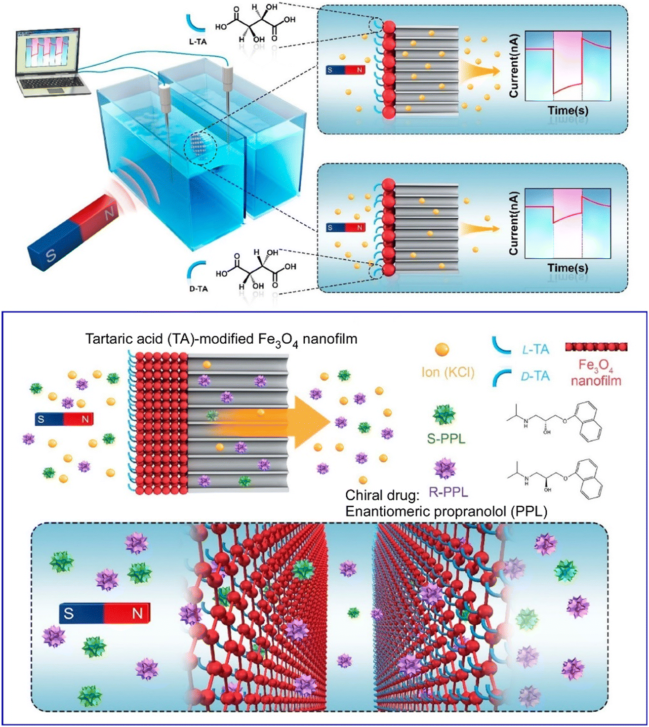 | ||
| Fig. 23 Magnetic field tuneable chiral ionic current generated by chiral magnetic Fe3O4 nanofilms acting on ion transport due to the different redistribution of electrons at the chiral-ferromagnetic interface caused by the magnetic field acting on differently configured chiral nanomaterials: chirality-dependent ion transport with magnetic gating (top) and detection and separation of propranolol (PPL) enantiomers (bottom). Reprinted with permission from ref. 79 copyright 2022 American Chemical Society. | ||
The self-assembly of nanocrystals into ordered superstructures constitutes a promising avenue for realizing emergent properties such as chirality, super-fluorescence, and band-like charge transport. However, conventional approaches are constrained by the inherent structural rigidity of nanocrystals, which typically yields tightly packed configurations and limits the formation of complex hierarchical architectures. A potential solution lies in scaling down nanocrystal dimensions to the molecular regime (∼2 nm), where their reduced size (termed nanoclusters) confers enhanced flexibility for structural engineering. Zang, Manna, Lu, and collaborators have demonstrated this principle through the fabrication of CsPbBr3 superstructures exhibiting circularly polarized photoluminescence, achieved via a two-step protocol involving nanocluster self-assembly followed by thermal annealing (Fig. 24).80 Critical to their methodology was the substitution of benzoic acid with the more hydrophobic 4-methylbenzoic acid during synthesis, which stabilized nucleated nanoclusters at ∼1.4 nm. This size reduction enabled the exploration of hierarchical assembly across multiple length scales: hexagonal packing at the nanoscale, wire bundles at the microscale, and millimeter-scale fiber-like morphologies. Remarkably, chirality emerged intrinsically without chiral ligands or templates, yielding dissymmetry factors of up to 0.1. Post-annealing, the superstructures retained chiral optical properties while exhibiting tunable photoluminescence (425 to 530 nm) and functional utility in light-emitting diodes (LEDs), which demonstrated electroluminescence polarization of 3 × 10⁻³. This work provided a viable alternative approach to creating multilevel chiral CsPbBr3 superstructures, which in principle can be extended to other materials. It may thus be possible to assemble intrinsically polarised emitters for LED and display applications.
 | ||
| Fig. 24 Fabrication of CsPbBr3 superstructures with circularly polarised photoluminescence using a two-step process involving self-assembly of nanoclusters (top) followed by annealing (bottom). Reprinted with permission from ref. 80 copyright 2025 Wiley-VCH. | ||
To conclude, chiral thin films have demonstrated considerable potential for applications, not only in CD and CPL, but also as combined multi-responsive platforms. On the one hand, the chemical nature of the nanocrystals can confer plasmonic or luminescence properties to the coatings. On the other hand, interfacing chiral nanocrystals with soft materials like block copolymers and liquid crystals provides films with signal modulation responses as a function of temperature, mechanical stretching and magnetic fields (Table 1).
| Nanocrystal system | Key mechanism for chirality | Main applications |
|---|---|---|
| 0D CdS arranged into 1D fiber bands (−2 μm wide) | Symmetry breaking during assemblyTop vs. bottom surface inversion | Chiroptical metamaterialsQuantum information technologies |
| 1D Ag/Au nanowires aligned on a 2D substrate by LbL | Structural anisotropy captured by graph descriptorsBond-percolation governs anisotropy | Polarization-sensitive coatingsModel for machine learning in chiral design |
| 1D Ag nanowires arranged in angled LbL bilayers | Interparticle plasmonic couplingTuning of CD intensity and spectral position | Chiral plasmonic metasurfacesChiral sensing platforms |
| 0D/1D (Au, Ag, Fe3O4, PbS) forming twisted multilayer superlattices | Geometric rotation of each layer yields overall helical stackChirality even with achiral building blocks | Large-area chiral photonic coatingsEnantioselective catalysis/sensing |
| 1D CdSe/CdS semiconductor nanorods | Tuning of CPL and CDIntrinsic rod luminescence couples to chiral arrangement | CPL devices3D displays, bioencoding, asymmetric catalysis |
| 0D Au NPs with intrinsic chirality (ligand-wrapped) | Ligand exchange to preserve gold NP chirality in a hydrophobic environmentMacroscopic CD achieved | Chiral plasmonic nanocompositesEnantioselective sensors and photonics |
6. Summary and perspectives
Nanoarchitectonics is a general and comprehensive concept of building functional materials from nano-units such as atoms, molecules and nanomaterials. The assembly of functional materials was examined across multiple scales, highlighting representative methodologies for structural control at distinct hierarchical levels. At the nanoscale, precision in nanocrystal fabrication enables tailored architectures with defined size, shape, and composition. Solution-processed thin film fabrication techniques provide scalable pathways to engineer material organization and interfacial properties. By bridging nanocrystals, which can be precisely engineered at the nanoscale, with macroscale processing strategies, a wide range of integrative approaches were developed to achieve functional coherence from molecular building blocks to device-relevant architectures.The presented examples encompass a diverse array of materials, methodologies, and applications within the realm of nanoarchitectonic material design. Key components include nanocrystals of 0D (including noble metal nanoparticles and nanocellulose), 1D (nanofibers, nanorods) and 2D nanomaterials that are either pre-formed or synthesised in situ, during the film processing. Fabrication techniques span adsorption approaches (e.g. Langmuir–Blodgett (LB) assembly, layer-by-layer (LbL) deposition, spin coating, automated one-drop assembly) and electrochemical approaches (electrosynthesis, EPD, electrodeposition), enabling precise structural control across scales. These methods facilitate the creation of sophisticated architectures such as hierarchical nanosheet arrays, twisted metastructures, and graph-theory-informed networks, alongside theoretical frameworks for predictive modeling. The applications highlighted range from high-sensitivity sensors and ultrathin catalytic interfaces to electromagnetic interference shielding, structurally colored cellulose films, water oxidation electrocatalysts, and asymmetric solid-state devices. A unifying theme across these examples is the rational integration of functionality into nanocrystal architectures. By leveraging nanoscale structural control-such as tailored crystallinity, surface chemistry, and chiral configurations, macroscopic surface platforms are engineered to exploit emergent nanophenomena, including quantum confinement, plasmonic coupling, and anisotropic charge transport. Notably, the strategic incorporation of chirality – through chiral nanocrystals, plasmonic metasurfaces, or helically anisotropic nanocomposites – represents an actively researched frontier. These advances hold promise for applications in enantioselective separation, asymmetric catalysis, chiral optical sensing, circularly polarized light detection, second-harmonic generation, and magnetically responsive devices.
This review has shown the synergy between nanocrystal design and solution-processed thin-film deposition, which enables scalable fabrication of multifunctional systems. This advantage can be extended beyond nanocrystals to a wide range of crystalline thin films. A unique example is the development of a chemical doping technique by Ishii, Yamashita and coworkers who exploited the redox reaction of benzoquinone and hydroquinone in air and in aqueous solution for doping control of polymeric semiconductor thin films (Fig. 25).81 This methodology employs a crystalline polymer-semiconductor thin film system characterized by molecular-scale voids capable of hosting dopant species. The incorporation of dopants into these interstitial sites is governed by proton-coupled electron transfer reactions, a process modulated by solution acidity (pH). The doping concentration exhibits precise pH dependence, enabling systematic control of electrical conductivity across approximately five orders of magnitude. The unique feature of this system is that the electrical conductivity of the crystalline polymer-semiconductor thin film can be coupled to an external process, proton-coupled electron transfer and a supramolecular doping phenomenon. In other words, the controllable physical properties of the crystal structure can be freely controlled by external processes. It is expected that this concept can be extended to systems such as thin films of nanocrystals. Indeed, the integration of external coupling processes with wet chemistry nanoarchitectonics represents a promising direction for dynamic control over nanocrystal-based thin films that will tune electronic, optical, or catalytic functionalities. These systems would benefit from hierarchical design principles, where predictable crystalline or supramolecular architectures enhance functional coherence across scales.
 | ||
| Fig. 25 Doping control of crystalline polymeric semiconductor thin films through the redox reaction of benzoquinone and hydroquinone in air and in aqueous solution. Reprinted with permission from ref. 81 copyright 2023 Springer-Nature. | ||
Although the current state of wet-chemistry nanoarchitectonics for nanocrystal-based thin films demonstrates impressive advances in structural control, scalability, and functional diversity, several limitations persist. Achieving defect-free, large-area films with precise nanoscale organization and integration of nanocrystals of varying dimensionality (0D, 1D, 2D) remains challenging, especially when translating laboratory assembly methods (e.g. LbL, LB…) to industrial scales. Issues of film uniformity, interfacial compatibility, and long-term stability under operational conditions will likely be a focal point for future research on adsorption-based nanocrystal film assembly. In addition, while electrochemical and in situ growth techniques offer comparatively better spatial control, they require further optimization for robust, reproducible, and environmentally benign processing. Priority areas for future research include the development of automated, high-throughput assembly systems, coupling external stimuli (e.g., pH, magnetic fields) for dynamic property tuning, and leveraging machine learning for predictive design and process optimization.
In particular, recent advancements in machine learning (ML) and artificial intelligence (AI) hold significant potential for optimizing such systems.82 These computational tools provide a framework for data-driven design, enabling precise control over nanocrystal assembly and thin-film performance. For example, a direction to combine nanoarchitectonics and materials informatics has been proposed.83 Data-driven discovery is thus expected to drastically accelerate the design and discovery of materials, nanomaterials and compounds with tailored properties.84 Emerging platforms (e.g. machine learning for materials design, MLMD) democratize AI-powered materials exploration by removing coding barriers and integrating model inference, surrogate optimization, and active learning, thus accelerating the optimization of complex chemical systems.84a The integration of ML with density functional theory (DFT) and high-throughput screening allows for fast and accurate property prediction that can achieve near-DFT accuracy at a fraction of the computational cost.84b,85 Other techniques, including transfer learning, multitask learning, and graph neural networks, are addressing the challenges of modeling complex polymer systems for further experimental validation.86 At a moment when multi-scale simulations, autonomous experimentation, and AI start converging, hidden structure–property relationships in materials science may be unveiled, which could support a new paradigm to accelerate the development of sustainable, high-performance nanomaterials for next-generation technologies.87
Ultimately, scalability remains a cornerstone for transitioning lab-scale innovations to industrial production. Wet-chemical methods, such as roll-to-roll deposition or automated LbL assembly, demonstrate compatibility with high-throughput manufacturing of large-area systems. By integrating these techniques with nanoarchitectonic principles, functional nanocrystal films such as chiral metasurfaces or structurally colored composites can be synthesized with uniform properties across macroscopic dimensions. For instance, controlled self-assembly of cellulose nanocrystals now achieves tunable photonic bandgaps and complex hierarchical structures for optical coatings and sensors.88In situ growth and precise alignment of perovskite nanocrystals within flexible matrices enable ultrastable, high-resolution scintillation films for advanced imaging technologies.89 Collectively, these innovations have the potential to accelerate the transition from laboratory-scale crystal films to industrial applications. Therefore, it is expected that wet-chemical nanoarchitectonics for nanocrystal-based films will pave the way for precise functional design of industry-compatible surface platforms. This convergence not only advances fundamental understanding of nanoscale phenomena but also paves the way for mass-produced, adaptive surfaces with programmable properties, poised to address global challenges in advanced technology (Table 2).
| Technique | Dimensionality | Key advantages | Representative applications |
|---|---|---|---|
| LB | 2D, 1D | Monolayer control at the air–water interfaceUniform coverageFine thickness tuning | Chiral plasmonic metasurfacesOptoelectronic devices |
| LbL | 0D, 1D, 2D | Precise multilayer stackingCompositional control (hybrid or hierarchical) Low-cost |
Electromagnetic interference shieldingHierarchical zeolite architectures for sensing/catalysis |
| Spin-coating | 0D, 2D | Fast film formationCompatible with various substrates | High-quality monolayer films on ITO/silicon2D device prototyping |
| Automated one-drop | 2D | Fast large-area depositionHigh packing density Highly oriented films |
Nanofilms and free-standing membranes for industrial scale manufacturing |
| Marangoni-effect | 2D | Ultrafast (≈10 s) large filmMinimal waste Easily scalable |
Transparent conductive filmsIridescent optical coatings |
| Roll-to-roll | 0D cellulose | Meter-long continuous depositionTunable structural color Excellent environmental stability (>1.5 years in water) |
Sustainable photonic pigmentsBiodegradable iridescent films |
| EPD | 0D, 2D | Thickness up to 1.5 μmVertical alignment for 2D Binder-free films |
UV-NIR blockingPhotoelectrochemical photodetectors |
| Electro-click | 0D | One-pot covalent reticulationFine thickness control | Granular electronicsTriggered drug-release coatings |
| Electrodeposition | Ionic precursor | In situ crystal growth with template-directed size controlDirect integration into device electrodes | Catalysts for water oxidationBattery and supercapacitor hybrids |
| Lithography-based epitaxial growth | Single-crystal perovskites | Flexible single crystals with low defect densityBandgap grading for optimized carrier transport | Flexible perovskite solar cellsHigh-stability optoelectronics |
Glossary
| AI | Artificial intelligence |
| COF(s) | Covalent organic framework(s) |
| CNC(s) | Cellulose nanocrystal(s) |
| CD | Circular dichroism |
| CPL | Circularly polarized luminescence |
| DFT | Density functional theory |
| DNA | Deoxyribonucleic acid |
| EBL | Electron beam lithography |
| EMI | Electromagnetic interference |
| EPD | Electrophoretic deposition |
| EQE | External quantum efficiency |
| FTO | Fluorine-doped tin oxide |
| HER | Hydrogen evolution reaction |
| ITO | Indium tin oxide |
| LED(s) | Light-emitting diode(s) |
| LbL | Layer-by-layer |
| LB | Langmuir–Blodgett |
| MOF(s) | Metal–organic framework(s) |
| MXene | 2D transition metal carbides/nitrides |
| OER | Oxygen evolution reaction |
| PEGDMA | Poly(ethylene glycol)dimethacrylate |
| PMMA | Polymethyl methacrylate |
| PVA | Poly(vinyl alcohol) |
| SAM | Self-assembled monolayer |
| SERS | Surface-enhanced Raman scattering |
| SEIRAS | Surface-enhanced infrared absorption spectroscopy |
Data availability
Because this is a review paper, new data are not included.Author contributions
G. R.: conceptualization, writing, review & editing. K. A.: conceptualization, writing, review & editing, funding acquisition.Conflicts of interest
There are no conflicts to declare.Acknowledgements
This study was partially supported by the Japan Society for the Promotion of Science KAKENHI (Grant Numbers JP25H00898 and JP23H05459). U. Ramirez Garcia is acknowledged for his editorial help with the revised manuscript.Notes and references
- (a) T. Fukushima, M. Higashi and M. Yamauchi, Bull. Chem. Soc. Jpn., 2023, 96, 1209–1215 CrossRef CAS; (b) T. Nakamura, Y. Kondo, N. Ohashi, C. Sakamoto, A. Hasegawa, S. Hu, M. A. Truong, R. Murdey, Y. Kanemitsu and A. Wakamiya, Bull. Chem. Soc. Jpn., 2024, 97, uoad025 CrossRef CAS; (c) G. Chen, M. Isegawa, T. Koide, Y. Yoshida, K. Harano, K. Hayashida, S. Fujita, K. Takeyasu, K. Ariga and J. Nakamura, Angew. Chem., Int. Ed., 2024, 63, e202410747 CrossRef CAS PubMed; (d) Y. Deng, M. Wei, Y. Lei, J. Lu, P. Peng, Y. Zhang and Z. Zheng, CrystEngComm, 2025, 27, 1055–1077 RSC; (e) M. A. Truong, T. Funasaki, Y. Adachi, S. Hira, T. Tan, A. Akatsuka, T. Yamada, Y. Iwasaki, Y. Matsushige, R. Kaneko, C. Asahara, T. Nakamura, R. Murdey, H. Yoshida, Y. Kanemitsu and A. Wakamiya, J. Am. Chem. Soc., 2025, 147, 2797–2808 CrossRef CAS PubMed.
- (a) J. Wang, F. Matsuzawa, N. Sato, Y. Amano and M. Machida, Bull. Chem. Soc. Jpn., 2023, 96, 1088–1098 CrossRef CAS; (b) U. Vattanasit, J. Kongpran and A. Ikeda, Sci. Total Environ., 2023, 904, 166745 CrossRef CAS PubMed; (c) S. Lim, C. Chen and M. Akiyama, Struct. Eng. Int., 2024, 35, 106–117 CrossRef; (d) N. Chen, M. Hu, L. Gou, L. Tan, D. Zhao and H. Feng, Bull. Chem. Soc. Jpn., 2024, 97, uoae030 CrossRef CAS; (e) Y. N. Myat, J. Kongpran, U. Vattanasit and S. Tanaka, Environ. Chem. Lett., 2024, 22, 2887–2911 CrossRef CAS.
- (a) T. Niwa, T. Tahara, C. E. Chase, F. G. Fang, T. Nakaoka, S. Irie, E. Hayashinaka, Y. Wada, H. Mukai, K. Masutomi, Y. Watanabe, Y. Cui and T. Hosoya, Bull. Chem. Soc. Jpn., 2023, 96, 283–290 CrossRef CAS; (b) S. Sando, Bull. Chem. Soc. Jpn., 2023, 96, 995–1002 CrossRef CAS; (c) P. H. Syaifie, M. A. F. Nasution, I. Rahmawati, E. Saepudin and T. A. Ivandini, Bull. Chem. Soc. Jpn., 2024, 97, uoad007 CrossRef CAS; (d) A. S. Tanwara and F. Meyer, CrystEngComm, 2025, 27, 736–748 RSC; (e) A. Javed, N. Kong, M. Mathesh, W. Duan and W. Yang, Sci. Technol. Adv. Mater., 2024, 25, 2345041 CrossRef PubMed.
- (a) G. Povie, Y. Segawa, T. Nishihara, Y. Miyauchi and K. Itami, Science, 2027, 356, 172–175 CrossRef PubMed; (b) Z. Sun, K. Ikemoto, T. M. Fukunaga, T. Koretsune, R. Arita, S. Sato and H. Isobe, Science, 2019, 363, 151–155 CrossRef CAS PubMed; (c) M. Sugiyama, M. Akiyama, Y. Yonezawa, M. Higashi, K. Nozaki and T. Okazoe, Science, 2022, 377, 756–759 CrossRef CAS PubMed; (d) K. Fuchibe, T. Fujita and J. Ichikawa, Bull. Chem. Soc. Jpn., 2024, 97, uoad024 CrossRef CAS; (e) Y. Nakao, Bull. Chem. Soc. Jpn., 2024, 97, uoae027 CrossRef CAS.
- (a) D. Guo, R. Shibuya, C. Akiba, S. Saji, T. Kondo and T. Nakamura, Science, 2016, 351, 361–365 CrossRef CAS PubMed; (b) A. Fukuoka, Bull. Chem. Soc. Jpn., 2023, 96, 1071–1076 CrossRef CAS; (c) S. Biswas, S. Das and Y. Negishi, Nanoscale Horiz., 2023, 8, 1509–1522 RSC; (d) A. Kuzume and K. Yamamoto, Bull. Chem. Soc. Jpn., 2024, 97, uoae022 CrossRef CAS; (e) K. Maeda, T. Motohashi, R. Ohtani, K. Sugimoto, Y. Tsuji, A. Kuwabara and S. Horike, Sci. Technol. Adv. Mater., 2024, 25, 2416384 CrossRef PubMed.
- (a) Y. Ashida, K. Arashiba, K. Nakajima and Y. Nishibayashi, Nature, 2019, 568, 536–540 CrossRef CAS PubMed; (b) S. Horike, Bull. Chem. Soc. Jpn., 2023, 96, 887–898 CrossRef CAS; (c) A. I. Osman, A. Ayati, P. Krivoshapkin, B. Tanhaei, M. Farghali, P.-S. Yap and A. Abdelhaleem, Coord. Chem. Rev., 2024, 514, 215900 CrossRef CAS; (d) Y. Mizumoto, M. Murao, Y. Yamazaki and T. Tsubomura, Bull. Chem. Soc. Jpn., 2024, 97, uoae035 CrossRef CAS; (e) J. J. Zakrzewski, M. Liberka, J. Wang, S. Chorazy and S. Ohkoshi, Chem. Rev., 2024, 124, 5930–6050 CrossRef CAS PubMed.
- (a) T. Yamamoto, A. Takahashi and H. Otsuka, Bull. Chem. Soc. Jpn., 2024, 97, uoad004 CrossRef CAS; (b) Y. Kim, K. Iimura and N. Tamaoki, Bull. Chem. Soc. Jpn., 2024, 97, uoae034 CrossRef CAS; (c) M. Kamigaito, Bull. Chem. Soc. Jpn., 2024, 97, uoae069 CrossRef CAS; (d) G. Gao, M. Hara, T. Seki and Y. Takeoka, Sci. Technol. Adv. Mater., 2024, 25, 2302795 CrossRef PubMed; (e) T. Kitao, Bull. Chem. Soc. Jpn., 2024, 97, uoae103 CrossRef CAS.
- (a) S. Datta, Y. Kato, S. Higashiharaguchi, K. Aratsu, A. Isobe, T. Saito, D. D. Prabhu, Y. Kitamoto, M. J. Hollamby, A. J. Smith, R. Dalgliesh, N. Mahmoudi, L. Pesce, C. Perego, G. M. Pavan and S. Yagai, Nature, 2020, 583, 400–405 CrossRef CAS PubMed; (b) O. Oki, H. Yamagishi, Y. Morisaki, R. Inoue, K. Ogawa, N. Miki, Y. Norikane, H. Sato and Y. Yamamoto, Science, 2022, 377, 673–678 CrossRef CAS PubMed; (c) H. Fujimoto, T. Hirao and T. Haino, Bull. Chem. Soc. Jpn., 2024, 97, uoad016 CrossRef CAS; (d) A. T. N. Doan and K. Sakurai, Bull. Chem. Soc. Jpn., 2024, 97, uoae042 CrossRef CAS; (e) T. Sugawara, M. Matsuo and T. Toyota, Bull. Chem. Soc. Jpn., 2025, 98, uoae134 CrossRef CAS.
- (a) S. D. K. Sundaram, M. M. Hossain, M. Rezki, K. Ariga and S. Tsujimura, Biosensors, 2023, 13, 1018 CrossRef PubMed; (b) T. Hayashi, Bull. Chem. Soc. Jpn., 2023, 96, 1331–1338 CrossRef CAS; (c) K. Murayama, H. Okita and H. Asanuma, Bull. Chem. Soc. Jpn., 2023, 96, 1179–1187 CrossRef CAS; (d) W. Yospanya, A. Matsumura, Y. Imasato, T. Itou, Y. Aoki, H. Nakazawa, T. Matsui, T. Yokoyama, M. Ui, M. Umetsu, S. Nagatoishi, K. Tsumoto, Y. Tanaka and K. Kinbara, Bull. Chem. Soc. Jpn., 2024, 97, uoae090 CrossRef CAS; (e) Y. Mizuuchi, Y. Hata, T. Sawada and T. Serizawa, Sci. Technol. Adv. Mater., 2024, 25, 2311052 CrossRef PubMed.
- (a) R. Kubota, Bull. Chem. Soc. Jpn., 2023, 96, 802–812 CrossRef CAS; (b) T. D. Bennett, S. Horike, J. C. Mauro, M. M. Smedskjaer and L. Wondraczek, Nat. Chem., 2024, 16, 1755–1766 CrossRef CAS PubMed; (c) S. Miyazaki, N. Ogiwara, C. A. Nagasaka, K. Takiishi, M. Inada and S. Uchida, Bull. Chem. Soc. Jpn., 2024, 97, uoae105 CrossRef CAS; (d) M. Minoshima, S. I. Reja, R. Hashimoto, K. Iijima and K. Kikuchi, Chem. Rev., 2024, 124, 6198–6270 CrossRef CAS PubMed; (e) M. Nakayama and W. Yoshida, ChemSusChem, 2025, 18, e202401907 CrossRef CAS PubMed.
- (a) R. P. Feynman, Eng. Sci., 1960, 23, 32–36 Search PubMed; (b) M. Roukes, Sci. Am., 2001, 285, 48–51 CrossRef CAS PubMed.
- (a) Y. Sugimoto, P. Pou, M. Abe, P. Jelinek, R. Pérez, S. Morita and Ó. Custance, Nature, 2007, 446, 64–67 CrossRef CAS PubMed; (b) K. Tada, Y. Hinuma, S. Ichikawa and S. Tanaka, Bull. Chem. Soc. Jpn., 2023, 96, 373–380 CrossRef CAS; (c) H. Hoelzel, S. Lee, K. Y. Amsharov, N. Jux, K. Harano, E. Nakamura and D. Lungerich, Nat. Chem., 2023, 15, 1444–1451 CrossRef CAS PubMed; (d) T. Nakamuro, Bull. Chem. Soc. Jpn., 2024, 97, uoae082 CrossRef CAS; (e) J. Hou, N. Xu, M. Z. H. Khan, L. Shan and T. Komeda, Appl. Surf. Sci., 2015, 694, 162852 CrossRef.
- (a) Y. Okawa and M. Aono, Nature, 2001, 409, 683–684 CrossRef CAS PubMed; (b) K. Terabe, T. Hasegawa, T. Nakayama and M. Aono, Nature, 2005, 433, 47–50 CrossRef CAS PubMed; (c) Y. Suzuki, A. Ikeda, S. Nakao, T. Nakato, K. Saito and J. Kawamata, Bull. Chem. Soc. Jpn., 2024, 97, uoae086 CrossRef CAS; (d) S. Kawai, O. Krejcí, T. Nishiuchi, K. Sahara, T. Kodama, R. Pawlak, E. Meyer, T. Kubo and A. S. Foster, Sci. Adv., 2020, 6, eaay8913 CrossRef CAS PubMed; (e) K. W. Sun, N. Cao, O. J. Silveira, A. O. Fumega, F. Hanindita, S. Ito, J. L. Lado, P. Liljeroth, A. S. Foster and S. Kawai, Sci. Adv., 2025, 11, eads1641 CrossRef CAS PubMed.
- (a) K. Kimura, K. Miwa, H. Imada, M. Imai-Imada, S. Kawahara, J. Takeya, M. Kawai, M. Galperin and Y. Kim, Nature, 2019, 570, 210–213 CrossRef CAS PubMed; (b) N. Oyamada, H. Minamimoto, T. Fukushima, R. Zhou and K. Murakoshi, Bull. Chem. Soc. Jpn., 2024, 97, uoae007 CrossRef CAS; (c) T. Tahara, Bull. Chem. Soc. Jpn., 2024, 97, uoae012 CrossRef CAS; (d) E. Kazuma, F. Prihatno, J. Jung, M. Trenary and Y. Kim, J. Phys. Chem. Lett., 2025, 16, 1810–1816 CrossRef CAS PubMed.
- (a) K. Saitow, Bull. Chem. Soc. Jpn., 2024, 97, uoad002 CrossRef CAS; (b) B. Roy and T. Govindaraju, Bull. Chem. Soc. Jpn., 2024, 97, bcsj.20230224 CrossRef CAS; (c) H. Gong, Y. Sakaguchi, T. Suzuki, M. Yanagisawa and T. Aida, Nature, 2024, 636, 92–99 CrossRef CAS PubMed; (d) K. Ariga, S. Akakabe, R. Sekiguchi, M. L. Thomas, Y. Takeoka, M. Rikukawa and M. Yoshizawa-Fujita, ACS Omega, 2024, 9, 22203–22212 CrossRef CAS PubMed.
- (a) K. Ariga, M. Nishikawa, T. Mori, J. Takeya, L. K. Shrestha and J. P. Hill, Sci. Technol. Adv. Mater., 2019, 20, 51–95 CrossRef CAS PubMed; (b) Y. Yamamoto, S. Kushida, D. Okada, O. Oki, H. Yamagishi and H. Hendra, Bull. Chem. Soc. Jpn., 2023, 96, 702–710 CrossRef CAS; (c) T. Kurita and K. Numata, Phys. Chem. Chem. Phys., 2024, 26, 28776–28792 RSC; (d) N. Chen, M. Hu, L. Gou, L. Tan, D. Zhao and H. Feng, Bull. Chem. Soc. Jpn., 2024, 97, uoae030 CrossRef CAS.
- (a) Z. Feng, X. Han, H. Wang, T. Tang and B. Xu, Chem, 2019, 5, 2442–2449 CrossRef CAS PubMed; (b) Y. Haketa, Y. Murakami and H. Maeda, Sci. Technol. Adv. Mater., 2024, 25, 2313958 CrossRef PubMed; (c) J. Song, K. Kawakami and K. Ariga, Adv. Colloid Interface Sci., 2025, 339, 103420 CrossRef CAS PubMed.
- (a) K. Sugamata, S. Kobayashi, A. Shirai, N. Amanokura and M. Minoura, Bull. Chem. Soc. Jpn., 2024, 97, uoae017 CrossRef CAS; (b) A. Yamauchi and N. Yanai, Acc. Chem. Res., 2024, 57, 2963–2972 CrossRef CAS PubMed; (c) K. Adpakpang, P. Ponchai, L. Pukdeejorhor, K. Faungnawakij and S. Bureekaew, Bull. Chem. Soc. Jpn., 2024, 97, uoae016 CrossRef CAS; (d) R. Rani, T. Ueda, K. Saeki, K. Toda and S. Ohira, Bull. Chem. Soc. Jpn., 2024, 97, uoae113 CrossRef CAS; (e) Z. Wang, Z. Yang, K.-I. Otake, J. Guo, X. Yang, Z. Xue, M.-S. Yao and S. Kitagawa, ChemElectroChem, 2025, 12, e202400525 CrossRef CAS.
- (a) J. Xiao, J. Chen, J. Liu, H. Ihara and H. Qiu, Green Energy Environ., 2023, 8, 1596–1618 CrossRef CAS; (b) H. Mabuchi, T. Irie, J. Sakai, S. Das and Y. Negishi, Chem. – Eur. J., 2024, 30, e202303474 CrossRef CAS PubMed; (c) W. Guo, J. Liu, H. Tao, J. Meng, J. Yang, Q. Shuai, Y. Asakura, L. Huang and Y. Yamauchi, Adv. Mater., 2024, 36, 2405399 CrossRef CAS PubMed; (d) D. Jiang, X. Xu, Y. Bando, S. M. Alshehri, M. Eguchi, T. Asahi and Y. Yamauchi, Bull. Chem. Soc. Jpn., 2024, 97, uoae074 CrossRef CAS; (e) T. Irie, S. Das, Q. Fang and Y. Negishi, J. Am. Chem. Soc., 2025, 147, 1367–1380 CrossRef CAS PubMed.
- (a) S. Mohanan, C. I. Sathish, T. J. Adams, S. Kan, M. Liang and A. Vinu, Bull. Chem. Soc. Jpn., 2023, 96, 1188–1195 CrossRef CAS; (b) J. M. Davidraj, C. I. Sathish, M. R. Benzigar, Z. Li, X. Zhang, R. Bahadur, K. Ramadass, G. Singh, J. Yi, P. Kumar and A. Vinu, Sci. Technol. Adv. Mater., 2024, 25, 2357062 CrossRef PubMed; (c) M. Yamamoto, S. Goto, R. Tang and K. Yamazaki, Chem. Sci., 2024, 15, 1953–1965 RSC; (d) A. Alowasheeir, M. Eguchi, Y. Fujita, K. Tsuchiya, R. Wakabayashi, T. Kimura, K. Ariga, K. Hatano, N. Fukumitsu and Y. Yamauchi, Bull. Chem. Soc. Jpn., 2024, 97, uoae099 CrossRef CAS; (e) J. Florek, M. Negoro, Y. Hu, K. Kanamori, K. Nakanishi and F. Kleitz, Adv. Funct. Mater., 2024, 35, 2409462 CrossRef.
- (a) K. Ariga, J. Li, J. Fei, Q. Ji and J. P. Hill, Adv. Mater., 2016, 28, 1251–1286 CrossRef CAS PubMed; (b) K. Ariga, Nanoscale Horiz., 2021, 6, 364–378 RSC.
- K. Ariga, X. Jia, J. Song, J. P. Hill, D. T. Leong, Y. Jia and J. Li, Angew. Chem., Int. Ed., 2020, 59, 15424–15446 CrossRef CAS PubMed.
- R. B. Laughlin and D. Pines, Proc. Natl. Acad. Sci. U. S. A., 2000, 97, 28–31 CrossRef CAS PubMed.
- K. Ariga, Bull. Chem. Soc. Jpn., 2024, 97, uoad001 CrossRef CAS.
- (a) M. Naguib, M. Kurtoglu, V. Presser, J. Lu, J. Niu, M. Heon, L. Hultman, Y. Gogotsi and M. W. Barsoum, Adv. Mater., 2011, 23, 4248–4253 CrossRef CAS PubMed; (b) M. Osada and T. Sasaki, Adv. Mater., 2012, 24, 210–228 CrossRef CAS PubMed; (c) Y. Kanemitsu, Nano Res., 2024, 17, 10536–10542 CrossRef CAS.
- (a) Y. Xia, Y. Xiong, B. Lim and S. Skrabalak, Angew. Chem., Int. Ed., 2009, 48, 60–103 CrossRef CAS PubMed; (b) S. Lee, T. Watanabe, F. M. Ross and J. H. Park, Small, 2024, 20, 2403969 CrossRef CAS PubMed.
- (a) N. Yamasaki, C. Matsuhashi, H. Oyama, H. Uekusa, J. Morikawa, M. Ryu, T. Tsujii, N. Nakayama, S. Obata, H. Goto, S. Maki and T. Hirano, Bull. Chem. Soc. Jpn., 2023, 96, 793–801 CrossRef CAS; (b) M. Shibuta and A. Nakajima, Nanoscale, 2024, 16, 12397–12405 RSC.
- (a) T. Takano, H. Masunaga, A. Fujiwara, H. Okuzaki and T. Sasaki, Macromolecules, 2012, 45, 3859–3865 CrossRef CAS; (b) H. Nobuoka, R. Tanaka, O. Urakawa and T. Inoue, Macromolecules, 2025, 58, 1380–1389 CrossRef CAS.
- T. Murata, K. Minami, T. Yamazaki, T. Sato, H. Koinuma, K. Ariga and N. Matsuki, Bull. Chem. Soc. Jpn., 2023, 96, 29–34 CrossRef CAS.
- (a) A. K. Geim and K. S. Novoselov, Nat. Mater., 2007, 6, 183–191 CrossRef CAS PubMed; (b) H. Endo, M. Mitsuishi and T. Miyashita, J. Mater. Chem., 2008, 18, 1302–1308 RSC.
- (a) T. Yokota, T. Kajitani, R. Shidachi, T. Tokuhara, M. Kaltenbrunner, Y. Shoji, F. Ishiwari, T. Sekitani, T. Fukushima and T. Someya, Nat. Nanotechnol., 2018, 13, 139–144 CrossRef CAS PubMed; (b) A. Yamamura, H. Fujii, H. Ogasawara, D. Nordlund, O. Takahashi, Y. Kishi, H. Ishii, N. Kobayashi, N. Niitsu, B. Blülle, T. Okamoto, Y. Wakabayashi, S. Watanabe and J. Takeya, Commun. Phys., 2020, 3, 20 CrossRef CAS.
- (a) M. Li, S. Ishihara, M. Akada, M. Liao, L. Sang, J. P. Hill, V. Krishnan, Y. Ma and K. Ariga, J. Am. Chem. Soc., 2011, 133, 7348–7351 CrossRef CAS PubMed; (b) M. Li and Y. Li, Acc. Chem. Res., 2023, 56, 3694–3703 CrossRef CAS PubMed.
- (a) L. Trotochaud, J. K. Ranney, K. N. Williams and S. W. Boettcher, J. Am. Chem. Soc., 2012, 134, 17253–17261 CrossRef CAS PubMed; (b) M. Yamagishi, S. Yamamoto, K. Okano, Y. Koshiba, S. Horike, K. Ishida, M. Horie and A. Mori, Bull. Chem. Soc. Jpn., 2024, 97, uoae095 Search PubMed.
- (a) Y. Yuan, G. Giri, A. L. Ayzner, A. P. Zoombelt, S. C. B. Mannsfeld, J. Chen, D. Nordlund, M. F. Toney, J. Huang and Z. Bao, Nat. Commun., 2014, 5, 3005 CrossRef PubMed; (b) M. Ishizaki, N. Koya, Y. Gotoh, K. Muramatsu and M. Kurihara, Bull. Chem. Soc. Jpn., 2024, 97, uoae071 CrossRef CAS.
- (a) J. Sagiv, J. Am. Chem. Soc., 1980, 102, 92–98 Search PubMed; (b) R. G. Nuzzo and D. L. Allara, J. Am. Chem. Soc., 1983, 105, 4481–4483 CrossRef CAS; (c) L. Strong and G. M. Whitesides, Langmuir, 1988, 4, 546–558 Search PubMed; (d) A. Akatsuka, M. Miura, G. Kapil, S. Hayase and H. Yoshida, Appl. Phys. Lett., 2024, 124, 241603 CrossRef CAS; (e) M. Zharnikov, Y. Shoji and T. Fukushima, Acc. Chem. Res., 2025, 58, 312–324 CrossRef CAS PubMed.
- (a) O. N. Oliveira Jr., L. Caseli and K. Ariga, Chem. Rev., 2022, 122, 6459–6513 CrossRef CAS PubMed; (b) R. Terui, Y. Otsuki, Y. Shibasaki and A. Fujimori, Bull. Chem. Soc. Jpn., 2024, 97, uoae050 CrossRef CAS; (c) S. Negi, M. Hamori, Y. Kubo, H. Kitagishi and K. Kano, Bull. Chem. Soc. Jpn., 2023, 96, 48–56 CrossRef CAS; (d) T. Ohata, K. Tachimoto, K. J. Takeno, A. Nomoto, T. Watanabe, I. Hirosawa and R. Makiura, Bull. Chem. Soc. Jpn., 2023, 96, 274–282 CrossRef CAS; (e) T. Mori, Sci. Technol. Adv. Mater., 2024, 25, 2334667 CrossRef PubMed; (f) J. Song, A. Jancik-Prochazkova, K. Kawakami and K. Ariga, Chem. Sci., 2024, 15, 18715–18750 RSC.
- (a) G. Decher, Science, 1997, 277, 1232–1237 CrossRef CAS; (b) G. Rydzek, Q. Ji, M. Li, P. Schaaf, J. P. Hill, F. Boulmedais and K. Ariga, Nano Today, 2015, 10, 138–167 CrossRef CAS; (c) K. Ariga, Y. Lvov and G. Decher, Phys. Chem. Chem. Phys., 2022, 24, 4097–4115 RSC; (d) E. Hasan, C. J. Lewis, J. G. Hernandez, P. Gentile and A. M. Ferreira, RSC Adv., 2025, 15, 13908–13923 RSC; (e) N. Fujisawa, L. Chen and M. Ebara, Langmuir, 2024, 40, 23895–23901 CrossRef CAS PubMed.
- (a) N. A. Kotov, I. Dekany and J. H. Fendler, J. Phys. Chem., 1995, 99, 13065–13069 CrossRef CAS; (b) Y. Lvov, K. Ariga, M. Onda, I. Ichinose and T. Kunitake, Langmuir, 1997, 13, 6195–6203 CrossRef CAS; (c) M. Fujita, A. Toyotama, T. Okuzono, H. Niinomib and J. Yamanaka, Soft Matter, 2024, 20, 985–992 RSC.
- (a) F.-X. Xiao, J. Miao and B. Liu, J. Am. Chem. Soc., 2014, 136, 1559–1569 CrossRef CAS PubMed; (b) T. Lee, K. Ohshiro, T. Watanabe, K. Hyeon-Deuk and D. Kim, Adv. Opt. Mater., 2022, 10, 2102781 CrossRef CAS; (c) K. Enomoto, R. Miranti, J. Liu, R. Okano, D. Inoue, D. Kim and Y.-J. Pu, Chem. Sci., 2024, 15, 13049–13057 RSC.
- (a) Y. Lvov, K. Ariga, I. Ichinose and T. Kunitake, J. Am. Chem. Soc., 1995, 117, 6117–6123 CrossRef CAS; (b) S. Yamaguchi, K. Chujo, N. Ohashi, K. Minamihata and T. Nagamune, Chem. – Eur. J., 2022, 28, e202103941 CrossRef CAS PubMed; (c) Z. Zhang, J. Zeng, W. Li and M. Matsusaki, Chem. Mater., 2024, 36, 1947–1956 CrossRef CAS.
- (a) Z. Liu, R. Ma, M. Osada, N. Iyi, Y. Ebina, K. Takada and T. Sasaki, J. Am. Chem. Soc., 2006, 128, 4872–4880 CrossRef CAS PubMed; (b) R. Hikichi, Y. Tokura, Y. Igarashi, H. Imai and Y. Oaki, Bull. Chem. Soc. Jpn., 2023, 96, 766–774 CrossRef CAS; (c) M. Bai, H. Wan, Y. Zhang, S. Chen, C. Lu, X. Liu, G. Chen, N. Zhan and R. Ma, Chem. Sci., 2024, 15, 16887–16907 RSC; (d) X. Tao, T. Tsugawa, K. Awaya, K. Hatakeyama, T. Ishihara and S. Ida, Inorg. Chem., 2025, 64, 882–891 CrossRef CAS PubMed.
- N. Sakai and T. Sasaki, Langmuir, 2022, 38, 12399–12407 CrossRef CAS PubMed.
- Y. Shi, E. Yamamoto, M. Kobayashi and M. Osada, ACS Appl. Mater. Interfaces, 2023, 15, 22737–22743 CrossRef CAS PubMed.
- Y. Shi, H. Li, H. Tsunematsu, H. Ozeki, K. Kano, E. Yamamoto, M. Kobayashi, H. Abe, C.-W. Chen and M. Osada, Small, 2024, 20, 2403915 CrossRef CAS PubMed.
- (a) R. Simancas, A. Chokkalingam, S. P. Elangovan, Z. Liu, T. Sano, K. Iyoki, T. Wakihara and T. Okubo, Chem. Sci., 2021, 12, 7677–7695 RSC; (b) J. Zhao, T. Wu, Q. He, H. Fang, M. Liu, Y. Liu, Z. Zhou, J. Zhang and W. Yang, Bull. Chem. Soc. Jpn., 2024, 97, uoae015 CrossRef CAS; (c) W. J. Roth, M. Opanasenko, M. Mazur, B. Gil, J. Čejka and T. Sasaki, Adv. Mater., 2024, 36, 2307341 CrossRef CAS PubMed; (d) T. Moteki, N. Tominaga and M. Ogura, Bull. Chem. Soc. Jpn., 2024, 97, uoae053 CrossRef CAS.
- C. Wang, N. Sakai, Y. Ebina, T. Kikuchi, J. Grzybek, W. J. Roth, B. Gil, R. Ma and T. Sasaki, Small, 2024, 20, 2308293 CrossRef CAS PubMed.
- H. K. Choi, A. Lee, M. Park, D. S. Lee, S. Bae, S.-K. Lee, S. H. Lee, T. Lee and T.-W. Kim, ACS Nano, 2021, 15, 829–839 CrossRef CAS PubMed.
- (a) E. Yashima, N. Ousaka, D. Taura, K. Shimomura, T. Ikai and K. Maeda, Chem. Rev., 2016, 116, 13752–13990 CrossRef CAS PubMed; (b) T. Ito, M. Nakagawa and T. Kawai, Bull. Chem. Soc. Jpn., 2024, 97, uoae075 CrossRef CAS; (c) S. Kobayashi, R. Nakazono, R. Okada, M. P. Schramm and T. Amaya, Bull. Chem. Soc. Jpn., 2024, 97, uoae098 CrossRef CAS; (d) R. Sekiya, S. Arimura, H. Moriguchi and T. Haino, Nanoscale, 2025, 17, 774–787 RSC.
- A. V. Gonzalez, M. Gonzalez and T. Hanrath, Sci. Adv., 2023, 9, eadi5520 CrossRef CAS PubMed.
- W. Wu, A. Kadar, S. H. Lee, H. J. Jung, B. C. Park, J. E. Raymond, T. K. Tsotsis, C. E. S. Cesnik, S. C. Glotzer, V. Goss and N. A. Kotov, Matter, 2025, 8, 101870 CrossRef CAS.
- W. Wu, Y. Battie, V. Lemaire, G. Decher and M. Pauly, Nano Lett., 2021, 21, 8298–8303 CrossRef CAS PubMed.
- H. Hu, S. Sekar, W. Wu, Y. Battie, V. Lemaire, O. Arteaga, L. V. Poulikakos, D. J. Norris, H. Giessen, G. Decher and M. Pauly, ACS Nano, 2021, 15, 13653–13661 CrossRef CAS PubMed.
- L. Chen, C. Hao, J. Cai, C. Chen, W. Ma, C. Xu, L. Xu and H. Kuang, Angew. Chem., Int. Ed., 2021, 60, 26276–26280 CrossRef CAS PubMed.
- B. E. Droguet, H.-L. Liang, B. Frka-Petesic, R. M. Parker, M. F. L. De Volder, J. J. Baumberg and S. Vignolini, Nat. Mater., 2022, 21, 352–358 CrossRef CAS PubMed.
- N. S. Mueller, E. Pfitzner, Y. Okamura, G. Gordeev, P. Kusch, H. Lange, J. Heberle, F. Schulz and S. Reich, ACS Nano, 2021, 15, 5523–5533 CrossRef CAS PubMed.
- C. Y. Zheng, Y. Yao, J. Deng, S. Seifert, A. M. Wong, B. Lee and C. A. Mirkin, ACS Nano, 2022, 16, 4813–4822 CrossRef CAS PubMed.
- W. Ge, F. Zhang, D. Wang, Q. Wei, Q. Li, Z. Feng, S. Feng, X. Xue, G. Qing and Y. Liu, Small, 2022, 18, 2107105 CrossRef CAS PubMed.
- J.-N. Yang, T. Chen, J. Ge, J.-J. Wang, Y.-C. Yin, Y.-F. Lan, X.-C. Ru, Z.-Y. Ma, Q. Zhang and H.-B. Yao, J. Am. Chem. Soc., 2021, 143, 19928–19937 CrossRef CAS PubMed.
- F. Sciortino, G. Rydzek and F. Boulmedais, Langmuir, 2023, 39, 11149–11165 CrossRef CAS PubMed.
- N. T. K. Nguyen, M. Dubernet, Y. Matsui, M. Wilmet, N. Shirahata, G. Rydzek, N. Dumait, M. A. Cortes, A. Renaud, S. Cordier, Y. Molard, F. Grasset and T. Uchikoshi, R. Soc. Open Sci., 2019, 6, 181647 CrossRef CAS PubMed.
- S. A. Bhakhar, P. M. Pataniya, M. Tannarana, G. K. Solanki and V. M. Pathak, Opt. Mater., 2022, 125, 112097 CrossRef CAS.
- (a) H.-F. Wang, L. Chen, H. Pang, S. Kaskel and Q. Xu, Chem. Soc. Rev., 2020, 49, 1414–1448 RSC; (b) P. Ganesan, A. Ishihara, A. Staykov and N. Nakashima, Bull. Chem. Soc. Jpn., 2023, 96, 429–443 CrossRef CAS; (c) P. Wang, J. Zheng, X. Xu, Y.-Q. Zhang, Q.-F. Shi, Y. Wan, S. Ramakrishna, J. Zhang, L. Zhu, T. Yokoshima, Y. Yamauchi and Y.-Z. Long, Adv. Mater., 2024, 36, 2404806 CrossRef CAS PubMed; (d) S. Yamada and T. Honda, Nanoscale, 2024, 16, 20027–20036 RSC.
- P. M. Pataniya, V. Patel and C. K. Sumesh, ACS Appl. Energy Mater., 2021, 4, 7891–7899 CrossRef CAS.
- J. Du, Y. Lu, J. Zhang, J. Wang, Y. Wang, M. Li and Q. Chen, ACS Omega, 2018, 3, 12495–12500 CrossRef CAS PubMed.
- G. Rydzek, D. Toulemon, A. Garofalo, C. Leuvrey, J.-F. Dayen, D. Felder-Flesch, P. Schaaf, L. Jierry, S. Begin-Colin, B. P. Pichon and F. Boulmedais, Small, 2015, 11, 4638–4642 CrossRef CAS PubMed.
- F. Sciortino, G. Rydzek, F. Grasset, M. L. Kahn, J. P. Hill, S. Chevance, F. Gauffre and K. Ariga, Phys. Chem. Chem. Phys., 2018, 20, 2761–2770 RSC.
- (a) X. Wang, K. Maeda, X. Chen, K. Takanabe, K. Domen, Y. Hou, X. Fu and M. Antonietti, J. Am. Chem. Soc., 2009, 131, 1680–1681 CrossRef CAS PubMed; (b) M. Inaba, R. Murase, T. Takeshita, K. Yano, S. Kosaka, N. Takahashi, N. Isomura, K. Oh-ishi, W. Yoshimune, K. Tsuchiya, T. Nobukawa and K. Kodama, ACS Appl. Mater. Interfaces, 2024, 16, 10295–10306 CrossRef CAS PubMed; (c) L. Fu, H. N. Nam, J. Zhou, Y. Kang, K. Wang, Z. Zhou, Y. Zhao, L. Zhu, R. Nandan, M. Eguchi, Q. M. Phung, T. Yokoshima, K. Wu and Y. Yamauchi, ACS Nano, 2024, 18, 27617–27629 CrossRef CAS PubMed; (d) Y. Shigeta, R. Asano, T. Kurihara, S. Amemori, T. Ida and M. Mizuno, J. Phys. Chem. C, 2025, 129, 6032–6040 CrossRef CAS.
- H. A. Raza, I. Karakaya and Ö. Dag, ACS Appl. Energy Mater., 2023, 6, 9681–9697 CrossRef CAS.
- (a) Y. Yamada, T. Nakamura, M. Endo, A. Wakamiya and Y. Kanemitsu, Appl. Phys. Express, 2014, 7, 032302 CrossRef CAS; (b) A. K. Cheetham, P. D. Bristowe, S. Tominaka and F. Wei, Mater. Horiz., 2024, 11, 1832–1837 RSC; (c) P.-J. Huang, I. Naruse and K. Taniguchi, Chem. Mater., 2024, 36, 7292–7298 CrossRef CAS; (d) C. Shi, J. Wang, X. Lei, Q. Zhou, W. Wang, Z. Yang, S. Liu, J. Zhang, H. Zhu, R. Chen, Y. Pan, Z. Tan, W. Liu, Z. Zhao, Z. Cai, X. Qin, Z. Zhao, J. Li, Z. Liu and W. Chen, Nat. Commun., 2015, 16, 3029 CrossRef PubMed.
- Y. Lei, Y. Chen, R. Zhang, Y. Li, Q. Yan, S. Lee, Y. Yu, H. Tsai, W. Choi, K. Wang, Y. Luo, Y. Gu, X. Zheng, C. Wang, C. Wang, H. Hu, Y. Li, B. Qi, M. Lin, Z. Zhang, S. A. Dayeh, M. Pharr, D. P. Fenning, Y.-H. Lo and S. Xu, Nature, 2020, 583, 790–795 CrossRef CAS PubMed.
- T. Nasir, L. Shao, Y. Han, R. Beanland, P. N. Bartlett and A. L. Hector, Nanoscale Adv., 2022, 4, 4798–4808 RSC.
- R. G. Bobade, U. T. Nakate, P. Roasiah, M. Ouladsmane, B. J. Lokhande and R. C. Ambare, Inorg. Chem. Commun., 2023, 154, 110998 CrossRef CAS.
- (a) T. Yamaguchi, T. Kimura, H. Matsuda and T. Aida, Angew. Chem., Int. Ed., 2004, 43, 6350–6355 CrossRef CAS PubMed; (b) Y.-B. Tian, K. Tanaka, L.-M. Chang, C. Wöll, Z.-G. Gu and J. Zhang, Nano Lett., 2023, 23, 5794–5801 CrossRef CAS PubMed; (c) S.-M. Jing, Z.-G. Gu and J. Zhang, J. Am. Chem. Soc., 2025, 147, 8948–8958 CrossRef CAS PubMed; (d) X. Nie, Y. Zhang, B. Wu, Z. Ye, F. Gao, Y. Chen, C. Wang, D. Zhu, P. Alam, Z. Qiu and B. Z. Tang, ACS Nano, 2025, 19, 11221–11229 CrossRef CAS PubMed.
- D. Grzelak, M. Tupikowska, D. Vila-Liarte, D. Beutel, M. Bagiński, S. Parzyszek, M. Góra, C. Rockstuhl, L. M. Liz-Marzán and W. Lewandowski, Adv. Funct. Mater., 2022, 32, 2111280 CrossRef CAS.
- N. Kowalska, F. Bandalewicz, J. Kowalski, S. Gómez-Graña, M. Bagiński, I. P. Santos, M. Grzelczak, J. Matraszek, J. Pérez-Juste and W. Lewandowski, ACS Appl. Mater. Interfaces, 2022, 14, 50013–50023 CrossRef CAS PubMed.
- M. Kim, J. Jeon, K. Pierce, D. Bukharina, W. Choi, J. Choi, D. Nepal, M. E. McConney, T. J. Bunning and V. V. Tsukruk, ACS Nano, 2024, 18, 25512–25521 CrossRef CAS PubMed.
- (a) S. Bao, S. Li, Z. Tang, Y. Wan, G. Zhou, Z. Yang, D. Sun, D. Ye and L. Zhu, J. Mater. Chem. C, 2025, 13, 9453–9464 RSC; (b) Y. Imai, Y. Mimura, Y. Motomura, R. Ikemura, M. Shizuma and M. Kitamatsu, Bull. Chem. Soc. Jpn., 2023, 96, 268–273 CrossRef CAS; (c) M. Ikeshita, Y. Tani, M. Kitahara, Y. Imai and T. Tsuno, Bull. Chem. Soc. Jpn., 2023, 96, 969–976 CrossRef CAS; (d) Y. H. Koo, Y. Tsutsui, M. Omoto, Y. Yomogida, K. Yanagi, Y. K. Kato, M. A. Hermosilla-Palacios, J. L. Blackburn and S. Seki, J. Phys. Chem. Lett., 2025, 16, 3232–3239 CrossRef CAS PubMed.
- L. Wen, Y. Xie, P. Yang, H. Zhang, J. Li, Z. Feng and G. Zou, Adv. Opt. Mater., 2024, 12, 2301308 CrossRef CAS.
- J. Cai, J. Zhao, X. Gao, W. Ma, D. Meng, H. Zhang, C. Hao, M. Sun, H. Kuang, C. Xu and L. Xu, ACS Nano, 2022, 16, 11066–11075 CrossRef CAS PubMed.
- B. Zhang, J. Xiao, Z. Xie, M. Jiang, H. Song, S. Toso, S. Zang, L. Manna and S. Lu, Angew. Chem., Int. Ed., 2025, 64, e202423272 CrossRef CAS PubMed.
- M. Ishii, Y. Yamashita, S. Watanabe, K. Ariga and J. Takeya, Nature, 2023, 622, 285–291 CrossRef CAS PubMed.
- (a) S. Wu, Y. Kondo, M. Kakimoto, B. Yang, H. Yamada, I. Kuwajima, G. Lambard, K. Hongo, Y. Xu, J. Shiomi, C. Schick, J. Morikawa and R. Yoshida, npj Comput. Mater., 2019, 5, 66 CrossRef; (b) K. Nakaguro, Y. Mitsuta, S. Koseki, T. Oshiyama and T. Asada, Bull. Chem. Soc. Jpn., 2023, 96, 1099–1107 CrossRef CAS; (c) K. Nakayama and K. Sakakibara, Sci. Technol. Adv. Mater., 2024, 25, 2351356 CrossRef PubMed; (d) T. Sadakane, K. Nakata, K. Suda and D. Yokogawa, Bull. Chem. Soc. Jpn., 2024, 97, uoae121 CrossRef CAS; (e) R. Tamura, K. Nagata, K. Sodeyama, K. Nakamura, T. Tokuhira, S. Shibata, K. Hammura, H. Sugisawa, M. Kawamura, T. Tsurimoto, M. Naito, M. Demura and T. Nakanishi, Sci. Technol. Adv. Mater., 2024, 25, 2388016 CrossRef PubMed.
- W. Chaikittisilp, Y. Yamauchi and K. Ariga, Adv. Mater., 2022, 34, 2107212 CrossRef CAS PubMed.
- (a) J. Ma, B. Cao, S. Dong, Y. Tian, M. Wang, J. Xiong and S. Sun, npj Comput. Mater., 2024, 10, 59 CrossRef; (b) I. Papadimitriou, I. Gialampoukidis, S. Vrochidis and I. Kompatsiaris, Comput. Mater. Sci., 2024, 235, 112793 CrossRef CAS.
- X. Liu, K. Yang, L. Zhang, W. Wang, S. Zhou, B. Wu, M. Xiong, S. Yang and R. Tan, Energy Mater. Adv., 2024, 5, 0131 CrossRef CAS.
- L. Gao, J. Lin, L. Wang and L. Du, Acc. Mater. Res., 2024, 5, 571–584 CrossRef CAS.
- Y. Ma, P. Xu, M. Li, X. Ji, W. Zhao and W. Lu, npj Comput. Mater., 2024, 10, 141 CrossRef.
- G. Chu, Acc. Mater. Res., 2024, 5, 1388–1400 CrossRef CAS.
- R. Li, W. Zhu, H. Wang, Y. Jiao, Y. Gao, R. Gao, R. Wang, H. Chao, A. Yu and X. Liu, npj Flexible Electron., 2024, 8, 31 CrossRef CAS.
| This journal is © The Royal Society of Chemistry 2025 |