
 Open Access Article
 This Open Access Article is licensed under a Creative Commons Attribution-Non Commercial 3.0 Unported Licence
Elucidating thin film growth mechanisms for high-performance II–VI photovoltaic semiconductors: simulation-driven insights and challenges
Chengchi
Cao
 and
Qi
An
*
and
Qi
An
*
Department of Materials Science and Engineering, Iowa State University, Ames, IA 50011, USA. E-mail: qan@iastate.edu
First published on 15th April 2025
Abstract
Thin film growth is a critical process in manufacturing photovoltaic semiconductors. However, defects such as grain boundaries and dislocations that form during film deposition can significantly impair device efficiency. A thorough understanding of the underlying mechanisms is therefore essential to improve film quality. In this review, we summarized recent advancements in understanding thin film growth mechanisms, with a focus on II–VI compound semiconductors, which are highly promising materials for photovoltaic applications. We highlight studies that have increasingly integrated atomistic simulations—such as molecular dynamics (MD) and kinetic Monte Carlo (kMC)—with experimental techniques to address the challenges inherent in thin film deposition. We further discuss critical factors influencing film quality, including deposition conditions, substrate interactions, and kinetic constraints. These insights contribute to a deeper understanding of thin film growth and may guide future efforts to optimize deposition techniques for high-performance photovoltaic materials.
 Qi An | Qi An has been an Associate Professor in the Department of Materials Science and Engineering at Iowa State University since 2022. His research primarily focuses on elucidating the processing and properties of materials—such as semiconductors and ceramics—through advanced computational approaches including machine learning, electronic structure calculations, and atomistic simulations. |
1. Introduction
Thin film growth involves the sequential deposition of atoms on a substrate, forming films with thicknesses ranging from a few nanometers to several micrometers.1 These films consist of metals, semiconductors, insulators, or composites, with their properties determined by the deposition process, material selection, and growth conditions.2,3 One of the most significant applications of thin films is in the semiconductor industry, where they are used to fabricate integrated circuits, transistors, and memory devices.4–6 In addition, thin-film technologies are employed in photovoltaic cells to improve energy conversion efficiency while reducing material consumption.7,8 Their versatility stems from their ability to enhance surface properties, such as hardness, corrosion resistance, and conductivity, without significantly altering the bulk properties of the substrate. This makes them invaluable for next-generation materials and devices across diverse scientific and industrial applications.Thin film growth can be achieved through various experimental methods, each tailored to specific applications and material requirements. Physical vapor deposition (PVD) uses vacuum-based techniques like evaporation and sputtering to deposit high-purity films, typically achieving thickness from a few nm to several μm at deposition rates of 1–10 nm per second.9 In contrast, chemical vapor deposition (CVD) relies on chemical reactions of gaseous precursors to produce uniform coatings, with variants like plasma-enhanced CVD enabling lower deposition temperatures. CVD does not require a high vacuum environment, allows for changes in precursor composition during deposition, and is particularly effective for coating 3D structures, recesses, and holes, often at high deposition rates.10–14 Atomic layer deposition (ALD), known as a bottom-up method,15 offers atomic-scale control ideal for producing ultra-thin films with precise composition control, high conformality, self-limiting reactions, and highly uniform thickness.16 Molecular beam epitaxy (MBE) provides unparalleled control over crystalline structure by using atomic or molecular beams in an ultra-high vacuum environment, achieving films of the highest quality with atomic layer control.17,18 Additionally, solution-based methods such as sol–gel processing, spin-coating, and dip-coating offer cost-effective, scalable, and low-temperature routes to thin film fabrication, though they often result in significant structural polydispersity (i.e., a broad distribution of thickness profiles), small lateral size, and chemical degradation.19–21 Collectively, these techniques drive innovations in semiconductors, optics, energy, and nanotechnology, with the selection of methods dependent on the desired film properties, cost considerations, and specific application requirements.
Mechanisms of thin film growth have been extensively studied, with Volmer–Weber growth (also referred to as nucleation and growth) serving as a classic example. In this mode, 3D nuclei form as gas phase atoms arrive uniformly on the substrate, spontaneously organizing into a crystal structure with an island shape (Fig. 1(a)). Following the initial nucleation, additional atoms diffuse across the surface to join these growing nuclei. Their incorporation depletes the local concentration of adsorbed atoms, establishing a gradient that further promotes atom attachment to the nuclei, thereby reinforcing the growth of islands. As deposition continues, these discrete crystal grains coalesce into a continuous film. This mechanism is typically observed when there is a significant difference in chemical properties or lattice parameters between the substrate and the thin film. For example, metals such as Au and Ag (ref. 22) are vapor-deposited onto ionic crystalline substrates such as NaCl or KCl, or Mn onto a Si substrate.23 Similarly, compound semiconductors such as AlN are deposited on Si substrates.24
 | ||
| Fig. 1 Schematic illustration of thin film growth modes with examples in oxide films, (a) Volmer–Weber (island growth), (b) Frank–van der Merwe (layer-by-layer growth), and (c) Stranski–Krastanov (layer-plus-island growth). | ||
Frank–van der Merwe growth involves the sequential, layer-by-layer deposition of atoms from the gas phase onto a substrate, as shown in Fig. 1(b). This mode typically occurs when the substrate and film share similar crystal structures and lattice constants—for instance, Ag on Cu and Au on Pd in metals,25 and GaAs on GaAs (homoepitaxy) and AlAs on GaAs in semiconductors.26 Such growth produces atomically flat films essential for artificial superlattices and heterostructure devices. However, even slight lattice mismatches can introduce dislocations that relax misfit strain, compromising interface quality. The allowable mismatch without dislocations depends on the material: up to 10% for metals, about 7% for semiconductors,27 and roughly 3% for ionic oxides.28
Stranski–Krastanov growth starts with the formation of a complete monolayer on the substrate, followed by the nucleation of three-dimensional islands (Fig. 1(c)), merging aspects of Frank–van der Merwe and Volmer–Weber modes.29 For example, high-temperature vapor deposition of Ag on Si (111) initially forms a monolayer (an R30° structure) before 3D islands develop, eventually coalescing into a continuous film. Similarly, the deposition of lanthanum strontium manganese oxide (LSMO) on LaAlO3 (ref. 30) follows this pattern. Notably, this mode can drive the self-assembly of quantum dots over large areas without lithography, opening avenues for novel applications.
The study of growth mechanisms,31 including Volmer–Weber, Frank–van der Merwe, and Stranski–Krastanov modes, is critical for controlling material properties at the atomic level, optimizing fabrication processes, and reducing defects in advanced II–VI semiconductors such as CdTe. CdTe stands out for its potential to enable low-cost, high-efficiency solar cells, being the only thin-film photovoltaic technology that surpasses crystalline Si in watt-per-cost efficiency.32,33 However, laboratory efficiencies for CdTe devices remain well below their theoretical maximum. A deep understanding of these growth processes is therefore essential for engineering high-quality thin films, nanostructures, and interfaces, which are important for next-generation photovoltaic devices.
In this highlight paper, we review the typical simulation methods for semiconductor thin film growth, comparing their advantages and limitations with a focus on II–VI semiconductors. We then discuss recent advances in this field, analyzing key findings and emerging trends. Our discussion centers on critical deposition and growth parameters—such as temperature, crystallographic orientation, and substrate conditions—that govern the structural quality, morphology, and defect formation in thin films. Finally, we outline the remaining challenges and propose potential directions for future research to advance thin film growth technologies.
2. Theoretical approaches in studying thin film growth
Theoretical modeling and computational simulations have become indispensable for studying the thin film growth mechanisms at the microscale. At the mesoscale, rate equations and phase field models treat thin films as continuous media, focusing on macroscopic parameters such as thickness, surface roughness, and growth rate.34 However, these approaches cannot capture the discrete nature of atomic-scale processes. At the atomic scale, methods such as lattice gas models, kinetic Monte Carlo (kMC) simulations, and molecular dynamics (MD) provide detailed insights into atomistic diffusion, nucleation, and adsorption–desorption dynamics.35–38Among these techniques, MD has emerged as a powerful tool for investigating the atomic-scale dynamics in real-time by solving Newton's equations of motion for interacting atoms. This method provides detailed atomistic perspectives on phenomena such as adatom diffusion, defect formation, nucleation processes, and surface reconstruction.39–42 The accuracy of MD simulations relies heavily on the interatomic potentials, including empirical potentials (e.g., Lennard-Jones, embedded atom method (EAM), Stillinger–Weber, and Tersoff potentials) and machine learning-based potentials for more complex systems. However, MD simulations are limited by short simulation timescales, typically on the order of nanoseconds. To overcome this, kMC simulations are frequently employed as a complementary method.
kMC simulations, when combined with rates derived from first-principles calculations such as density functional theory (DFT), enable long-time and large-scale modeling of thin-film growth processes.43 By incorporating activation energies and diffusion barriers, kMC simulations can accurately capture rare events and thermally activated processes that occur over microsecond to second timescales, which are inaccessible to MD simulations due to computational constraints.
In recent years, hybrid approaches that combine MD and kMC have been developed to leverage their respective strengths. MD simulations provide insights into atomic-scale dynamics,44 while kMC excels at modeling long-time-scale phenomena such as nucleation,45 growth kinetics, and microstructural evolution.46 Together, these methods offer a comprehensive framework for understanding complex processes such as thin film growth.
3. Epitaxy thin film growth and its relevant variables
Deposition and growth conditions critically determine the formation and structural quality of thin films by directly influencing growth dynamics, crystallinity, and defect formation. Temperature, substrate termination, and crystallographic orientation are key factors that affect atomic mobility, nucleation, and defect densities. For instance, temperature governs adatom diffusion and surface morphology, with variations leading to differences in stacking fault formation, dislocation densities, and phase composition. Similarly, substrate termination (e.g., Cd-terminated and Te-terminated surfaces in CdTe growth) impacts atomic reactivity and bonding configurations, thereby affecting growth behavior and defect distribution. Moreover, crystallographic orientation determines the arrangement and evolution of defects, including dislocations, stacking faults, and grain boundaries. MD simulations and other computational modeling provide critical insights into these interdependencies, guiding the optimization of deposition parameters for producing high-quality thin films with precisely controlled structural properties. The details of these effects are discussed below.3.1 Temperature
Temperature plays a pivotal role in epitaxial growth and the quality of semiconductor thin films by controlling adatom mobility and surface diffusion. At higher temperatures, adatoms gain sufficient kinetic energy to migrate to stable lattice sites, promoting layer-by-layer growth and reducing surface roughness. In contrast, lower temperatures hinder adatom diffusion, resulting in rougher films with a higher density of defects and amorphous regions. Temperature also influences nucleation dynamics; elevated temperatures tend to produce fewer, larger islands that merge into smoother films, whereas lower temperatures lead to numerous smaller islands and irregular morphologies. Additionally, optimal temperature conditions facilitate elastic strain relaxation, thereby minimizing dislocations, while inappropriate temperatures can trigger plastic relaxation and generate structural defects such as stacking faults and twin boundaries. Although higher substrate temperatures generally improve crystallinity and reduce dislocation density, they can also induce stacking faults and twinning on reactive surfaces like Te-terminated CdTe, where competing zinc-blende and wurtzite phases coexist. Thus, precise control of temperature, in combination with flux ratios and deposition rates, is essential for fabricating high-quality thin films with balanced composition and minimal defects.Li et al.47 employed MD simulations and force-bias Monte Carlo (fbMC) simulations to investigate the growth dynamics of CdTe films. They developed a machine learning force field (ML-FF) to accurately model atomic interactions in MD simulations. Using CdTe substrates with both (111) Te-terminated and (111) Cd-terminated surfaces, isolated Cd and Te atoms were allowed to adsorb onto the substrates, with the fbMC method efficiently relaxing the adsorbates and forming surface structures. Fig. 2 illustrates the growth dynamics over a temperature range from 400 to 1000 K. As temperature increases, the number of stacking faults (represented by orange atoms) increases drastically due to the competitive formation between CdTe zinc-blende and wurtzite structures. Notably, at low temperatures, the (111) Cd-terminated surface (Fig. 2(a)) exhibits significantly fewer stacking faults compared to the (111) Te-terminated surface (Fig. 2(b)), a difference attributed to the higher reactivity of the (111) Te-terminated surface.
 | ||
| Fig. 2 Layer structures of CdTe homoepitaxial films grown on (a) (111) Cd-terminated and (b) (111) Te-terminated surfaces across a range of substrate temperatures: 400 K, 600 K, 800 K, and 1000 K. (c) Overall crystallinity and (d) WZ-crystallinity of the CdTe homoepitaxial layers as a function of substrate temperature. (e) Free energy difference of CdTe zinc-blende and wurtzite structures as a function of temperature. Atoms are color-coded for clarity: light gray represents disordered atoms; blue denotes diamond-structured atoms; cyan and green indicate the first and second neighbors of diamond-structured atoms; orange represents hexagonal-structured atoms; and yellow and purple denote the first and second neighbors of hexagonal-structured atoms. The substrate region is marked by a shaded area (copyright from ACS Crystal Growth and Design).47 | ||
The substrate temperature also greatly influences the crystallization quality of CdTe films. As shown in Fig. 2(c) and (d), both the overall crystallinity and the WZ-crystallinity ratio of CdTe homoepitaxial layers increase with substrate temperature, stabilizing at ∼0.80 for (111) Cd and ∼0.82 for (111) Te layers above 600 K. This arises from the enhanced adatom mobility at elevated temperatures, which allows atoms to efficiently reach lower energy lattice sites before encountering additional vapor-phase species. Furthermore, as illustrated in Fig. 2(e), the reduced free energy difference between zinc-blende and wurtzite structures at higher temperatures further favors wurtzite formation, thereby promoting stacking fault layers and reducing their spacing. Consequently, higher growth temperature yields films with improved crystallinity, in line with previous studies.48 CdTe homoepitaxial layers typically exhibit a zinc-blende structure interspersed with stacking faults that form wurtzite regions.
Another study also shows the effect of temperature on the crystallization quality of thin films. Hew et al.49 utilized MD simulations with Stillinger–Weber (SW) potential, tailored for II–VI compounds Zn–Cd–Hg–S–Se–Te, to examine the effects of substrate temperature on the crystallinity and sticking coefficient of Hg1−xCdxTe (MCT) on a perfect (211) Te-terminated CdTe substrate during MBE growth. In their simulations, as shown in Fig. 3(a), vapor species (including Cd, Hg, and Te2 dimers) were randomly injected above the substrate with a constant kinetic energy per atom. Fig. 3(c) revealed that the Hg sticking coefficient decreases exponentially with increasing substrate temperature at a growth rate of 0.03–0.07 nm ns−1 and a fixed Hg/Te flux ratio of 1.4, trends that align well with experimental observations.50 Their results also indicate that the optimal substrate temperature is growth rate dependent: a higher deposition rate necessitates higher substrate temperatures to provide adatoms with sufficient energy to migrate to their lowest-energy sites before subsequent atoms arrive. Additionally, substrate temperature significantly affects both the crystallinity and Cd composition (x) of the films, as shown in Fig. 3(d). Under fixed growth rate and Hg/Te flux conditions, an optimum temperature of 758 K was found to yield a crystallinity of 0.84 and a Cd composition of 0.3. Temperatures below this optimum result in excess Hg deposition, whereas higher temperatures promote excess Te incorporation (Fig. 3(b)). Although the SW potential successfully captures these trends, it does not fully reproduce the experimental structure, which is predominantly amorphous with traces of FCC and HCP phases (only counting Te atoms).
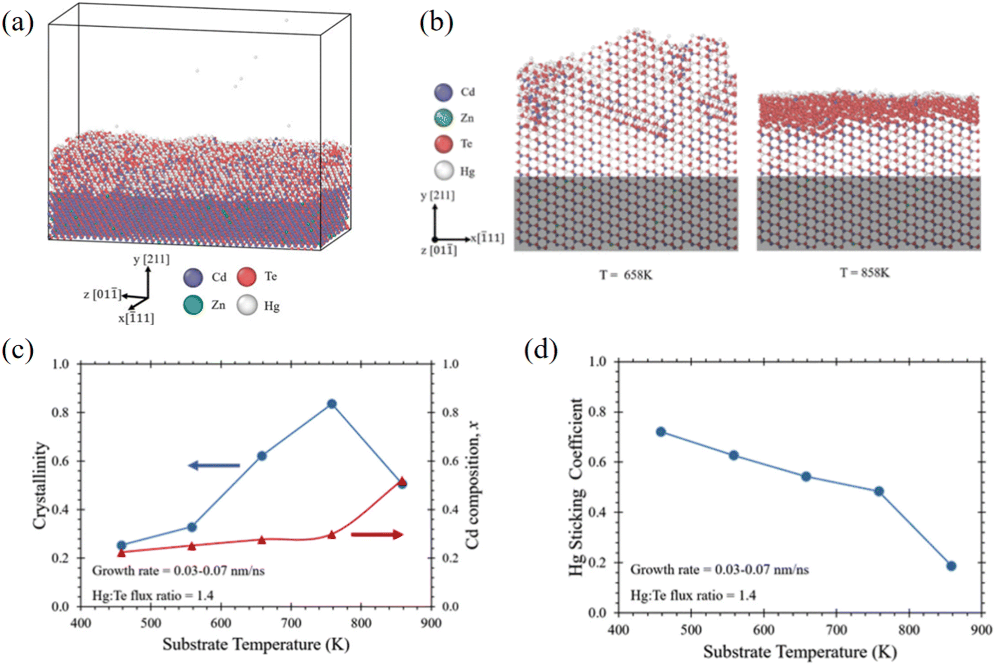 | ||
| Fig. 3 (a) Hg1−xCdxTe deposition process. (b) MCT grown on a perfect (211) Te-terminated Cd0.96Zn0.04Te substrate at temperatures of 658 K and 858 K. (c) Hg sticking coefficient as a function of substrate temperature. (d) Crystallinity and Cd composition as a function of substrate temperature (copyright from ACS Applied Electronic Materials).49 | ||
In another study, Almeida et al.51 used MD with SW potential52 to investigate the effects of temperature on wurtzite CdS homoepitaxial growth. In their simulations, Cd and S atoms were randomly deposited onto a Cd-terminated CdS[0001] substrate. The findings show that films grown at higher temperatures exhibit lower dislocation length densities (Fig. 4(a)). Additionally, although elevated temperatures accentuate the impact of the deposition rate on dislocation density, they do not eliminate dislocation entirely (Fig. 4(b)). These results reveal the thermal sensitivity of dislocation formation and corroborate previous studies on temperature-dependent defect reduction.49
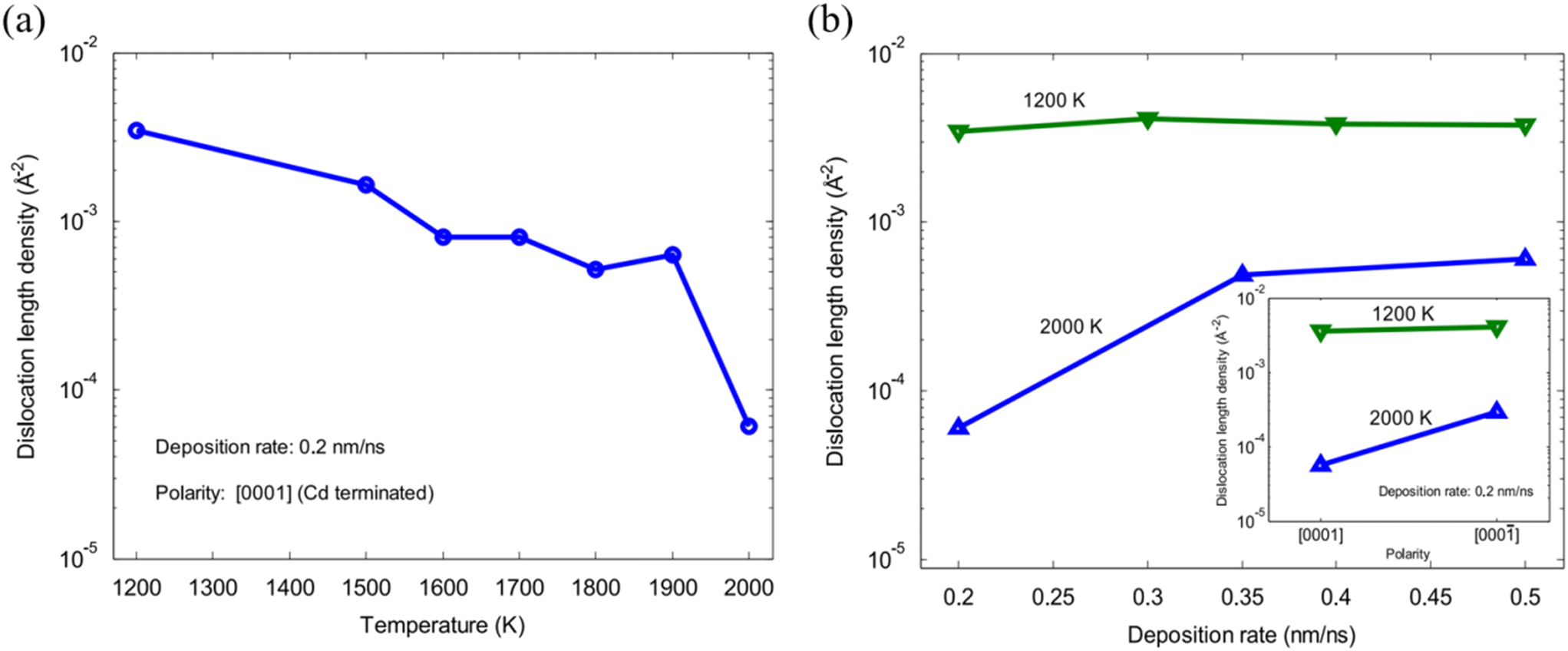 | ||
Fig. 4 (a) Dislocation length density as a function of substrate temperatures at constant deposition rate. (b) Dislocation length density as a function of different deposition rates at 1200 K and 2000 K. The inset shows the dislocation length density for different polarities: [0001] for Cd-terminated and [000![[1 with combining macron]](https://www.rsc.org/images/entities/char_0031_0304.gif) ] for S terminated surfaces at 1200 K and 2000 K (copyright from Elsevier, Journal of Crystal Growth).51 ] for S terminated surfaces at 1200 K and 2000 K (copyright from Elsevier, Journal of Crystal Growth).51 | ||
3.2 Substrate effect: heteroepitaxy vs. homoepitaxy
The choice of substrate, whether heteroepitaxial or homoepitaxial, significantly influences the quality and properties of epitaxial films. Chavez et al.53 used MD simulations with Zn–Cd–Hg–S–Se–Te SW potential54 to investigate the growth of CdTe films on CdTe and CdS substrates containing pre-existing stacking faults, double positioning (DP) twins, and lamellar twin boundaries. Growth simulations were achieved by randomly injecting Cd and Te adatoms to the surface at a constant temperature of 1200 K with a stoichiometric vapor ratio of Cd/Te = 1![[thin space (1/6-em)]](https://www.rsc.org/images/entities/char_2009.gif) :1. The simulations reveal distinct behaviors of defect evolution during the growth of CdTe films under homoepitaxy and heteroepitaxy conditions. While DP and lamellar twin boundaries propagate consistently in both homogeneous and heterogeneous cases, stacking faults were found to propagate only in homogeneous cases. Notably, narrow stacking faults, confined by interacting Shockley partial dislocations, only propagate into the thin film up to a critical thickness before collapsing, leaving behind defect-free crystal regions. For homogeneous cases, the thin films exhibit high crystal quality; in contrast, heterogeneous cases develop regions dominated by WZ phase along with interfacial misfit and threading dislocations to accommodate the lattice mismatch. The DP and lamellar twins are highly reproducible despite the existence of lattice distortions and mismatch, though they disappear at grain boundaries. These findings provide important insight into defect interactions and propagation during thin film growth, helping to control epilayer grain boundaries and crystal quality during thin film growth.
:1. The simulations reveal distinct behaviors of defect evolution during the growth of CdTe films under homoepitaxy and heteroepitaxy conditions. While DP and lamellar twin boundaries propagate consistently in both homogeneous and heterogeneous cases, stacking faults were found to propagate only in homogeneous cases. Notably, narrow stacking faults, confined by interacting Shockley partial dislocations, only propagate into the thin film up to a critical thickness before collapsing, leaving behind defect-free crystal regions. For homogeneous cases, the thin films exhibit high crystal quality; in contrast, heterogeneous cases develop regions dominated by WZ phase along with interfacial misfit and threading dislocations to accommodate the lattice mismatch. The DP and lamellar twins are highly reproducible despite the existence of lattice distortions and mismatch, though they disappear at grain boundaries. These findings provide important insight into defect interactions and propagation during thin film growth, helping to control epilayer grain boundaries and crystal quality during thin film growth.
3.3 Te/Cd-terminated surface effect
The growth behavior of semiconductor thin films is profoundly influenced by the atomic arrangement and chemical nature of the substrate surface. Variations in surface termination, such as Cd-terminated or Te-terminated configurations, result in distinct growth dynamics due to differences in bonding strength and atomic reactivity. These differences impact critical processes such as nucleation, diffusion, and defect formation during deposition. By employing advanced computational methods, including MD and kMC simulations, researchers have gained valuable insights into optimizing deposition conditions for improved film quality and reduced defect densities.In a related study, Yu et al.55 employed MD simulations with SW potential56 specializing for II–VI elements52 to investigate the deposition of CdxTey clusters onto the wurtzite CdS surfaces with Cd- and S-terminated (111) facets. They identified six distinct impact scenarios—illustrated in Fig. 5(a)—by performing over 1200 simulations to ensure robust statistics. The results (Fig. 5(b)) indicate that Cd atoms are more readily sputtered from the surface than Te atoms, particularly on Cd-terminated facets. Deposited clusters are more likely to be reflected than sputtered, and a higher sticking probability is observed on S-terminated surfaces. Furthermore, increasing the deposition energy generally leads to more deposited atoms replacing surface atoms, fewer atoms remaining on the surface layer, and an increased number of interstitial defects.
 | ||
| Fig. 5 (a) The illustration graph for the 6 cases of the final states after impact. (b) Energetic impact results of small CdxTey (x, y = 0, 1) clusters on wurtzite (111) Cd-terminated and S-terminated CdS surfaces (copyright from Elsevier, Nuclear Instruments and Methods in Physics Research B).55 | ||
Yu et al.57 applied an on-the-fly kMC method using analytical bond-order potentials (BOPs)58,59 specifically developed for the CdTe binary system60,61 to simulate thin film growth on Cd- and Te-terminated surfaces. On the Te-terminated (111) surface, the CdTe clusters typically “lay down” such that Cd and Te atoms initially align at the same height. These clusters then form a mixed-species layer with a zig-zag chain morphology, from which Te atoms subsequently migrate to form an additional upper layer, resulting in a double-layer structure. In contrast, on the Cd-terminated (111) surface, the Cd and Te atoms adopt a “stand up” configuration with atoms at different heights, and the double-layer structure forms immediately after deposition. Moreover, while the deposited clusters tend to remain intact and stoichiometric on Te-terminated surfaces, they are more prone to dissociation and exhibit non-stoichiometry on Cd-terminated surfaces. Over an equivalent simulation period, the final lattice on Cd-terminated surfaces contained fewer atoms than that on Te-terminated surfaces, indicating a slower growth rate, even though atomic diffusion was more rapid on the Cd-terminated surfaces.
In Li et al.'s47 research work, which has been mentioned in the Temperature part, they studied CdTe film growth using MD and force-bias Monte Carlo simulations with an ML-FF. They deposited isolated Cd or Te atoms on CdTe substrates with (111) Te- and (111) Cd-terminated surfaces and found that homoepitaxial growth on (111) Te surfaces produced more pronounced planar defects, likely due to higher surface reactivity. In addition, the higher WZ-crystallinity ratio is observed in (111) Te-terminated layers compared with (111) Cd-terminated layers. As shown in Fig. 2(d), there is a clear propensity for lamella twin formation on these surfaces, likely due to their increased lateral growth and reactivity, a mode similar to the Frank–van der Merwe (layer-by-layer) mechanism. Indeed, the (111) Te-terminated surface, with a surface energy of 0.60 J m−2, leads to reduced stacking fault spacing compared to the 0.35 J m−2 of the (111) Cd-terminated surface.
3.4 Orientation
Recent MD studies on CdTe and CdS thin films highlight the critical influence of substrate crystallographic orientation on thin film growth and defect formation.62–64 Specific orientations can reduce misfit dislocation densities by optimizing interfacial properties and minimizing lattice mismatch strain energies. For example, films grown on {112} zinc-blende (ZB) and certain hexagonal wurtzite (WZ) surfaces exhibit superior crystallinity and lower defect densities, whereas orientations such as {0010} WZ and {111} ZB tend to generate higher density defects, including stacking faults, vacancies, and twins.In a study by Zhou et al.,64 MD simulations on vapor deposition using a Zn–Cd–Hg–S–Se–Te SW potential52 were employed to analyze CdTe films grown on{112} zinc-blende (ZB) CdS surfaces. Contrary to the anticipated epitaxial growth along the <112> direction, the CdTe films preferentially adopted a <331> orientation. Atomistic modeling revealed that this deviation arises from reduced misfit dislocation energies, highlighting the role of substrate orientation in modulating Burgers vectors and strain energy relaxation. These insights offer promising strategies for optimizing thin film growth and defect engineering.
Chavez et al.65 further explored the impact of substrate orientation by using MD simulations with the same multi-component SW potential52 to investigate the CdTe thin films deposited on eight distinct wurtzite (WZ) and ZB CdS substrate orientations. Their findings demonstrate that substrate orientation decisively influences the distribution and morphology of film defects, such as polytypism, grain boundaries, and dislocations, with dislocation lines displaying three unique patterns depending on the crystallographic orientation of the substrate.
As shown in Fig. 6(a), structural analysis revealed that all the samples exhibited polytypism, with coexisting wurtzite and zinc blende domains. Although most epilayers predominantly replicated the substrate's lattice structure, films grown on the {11![[2 with combining macron]](https://www.rsc.org/images/entities/char_0032_0304.gif) } surfaces deviated from this behavior. Detailed examination of lattice defects (Fig. 6(b))—including point defects, stacking faults, dislocations, and grain boundaries—showed that the dislocation density strongly depends on the substrate's crystallographic orientation. Films grown on the hexagonal surfaces {0001} and {111} displayed higher defect densities compared to those on rectangular surfaces ({100, {11}, {10} and {010}). Notably, films deposited on {110} and miscut surfaces deviated from this trend, showing higher defect densities. These findings corroborate earlier studies employing DFT, which identified optimal growth conditions based on surface stability analyses.51,66 Dislocation morphology was observed to vary distinctly with substrate orientation and could be categorized into three primary types. For films grown on {11} substrates, dislocations remained localized at the interface (Fig. 6(c)). This behavior indicates a highly effective strain-relief mechanism that mitigates the lattice mismatch, thereby preventing the formation of misfit dislocations. In contrast, films grown on {100}, {110}, {10}, {010}, and
} surfaces deviated from this behavior. Detailed examination of lattice defects (Fig. 6(b))—including point defects, stacking faults, dislocations, and grain boundaries—showed that the dislocation density strongly depends on the substrate's crystallographic orientation. Films grown on the hexagonal surfaces {0001} and {111} displayed higher defect densities compared to those on rectangular surfaces ({100, {11}, {10} and {010}). Notably, films deposited on {110} and miscut surfaces deviated from this trend, showing higher defect densities. These findings corroborate earlier studies employing DFT, which identified optimal growth conditions based on surface stability analyses.51,66 Dislocation morphology was observed to vary distinctly with substrate orientation and could be categorized into three primary types. For films grown on {11} substrates, dislocations remained localized at the interface (Fig. 6(c)). This behavior indicates a highly effective strain-relief mechanism that mitigates the lattice mismatch, thereby preventing the formation of misfit dislocations. In contrast, films grown on {100}, {110}, {10}, {010}, and  rectangular surfaces (Fig. 6(d) and (e)) exhibited dislocations that initiated at the interface but extended toward the surface. Films grown on hexagonal surfaces such as WZ {0001} and ZB {111} formed an interconnected dislocation network at the interface, which propagated throughout the film.
 | ||
| Fig. 6 (a) Lattice structure percentage and (b) dislocation density for all simulated growths. Polytypism and misfit dislocations were observed in all cases. Dislocation configurations in (c) CdTe on ZB (11) CdS, (d) CdTe on WZ (100) CdS, and (e) CdTe on WZ (0001) CdS substrate surfaces (figures from ref. 65, licensed under a Creative Commons Attribution 4.0 License).65 | ||
Almeida et al.51 investigated the temperature effects on wurtzite CdS homoepitaxial growth using MD simulations with a Stillinger–Weber potential. In their simulations, Cd and S atoms were randomly deposited on a Cd-terminated CdS [0001] substrate. Consistent with thermodynamic predictions, substrates with rectangular geometries, including [11] ZB, [100] WZ, [110] WZ, [110] ZB, [010] ZB and  ZB, yielded highly crystalline films with minimal point defects (Fig. 7(a)–(f)). In contrast, substrates with hexagonal geometries ([0001] WZ and [111] ZB) produced films with a higher density of defects, including anti-site defects, vacancies, stacking faults, twinning, and polytypism (Fig. 7(g) and (h)). Structural analysis further identified the presence of both WZ and ZB domains and their associated grain boundaries during hexagonal growth. Dislocation analysis revealed that the predominant defects were Shockley partials—with a Burgers vector of 1/6〈112〉—and full dislocations—with a Burgers vector of 〈0001〉 for the ZB and WZ families, respectively.
 | ||
Fig. 7 Atomistic visualizations of MD simulations for CdS homoepitaxial growth along (a) [100] WZ, (b) [110] WZ, (c) [110] ZB, (d) [010] ZB, (e)  , (f) [11] ZB, (g) [0001] WZ and (h) [111] ZB directions. Shaded regions represent the initial substrate (copyright from Elsevier, Journal of Crystal Growth).51 , (f) [11] ZB, (g) [0001] WZ and (h) [111] ZB directions. Shaded regions represent the initial substrate (copyright from Elsevier, Journal of Crystal Growth).51 | ||
These results highlight the necessity of optimizing substrate orientations and deposition parameters to achieve superior crystal quality in II–VI semiconductors.
4. kMC simulations on thin film growth
kMC is a computational simulation technique widely used to model the dynamic evolution of systems at atomic and molecular scales over extended time periods. Unlike traditional MD simulations—which resolve atomic trajectories in fine detail over short intervals—kMC focuses on stochastic processes and the sequence of rare events that drive system changes. This method is particularly well suited for studying thin-film growth, diffusion processes, and defect formation, as it statistically captures atomistic events such as adsorption, desorption, and surface diffusion without being limited by short simulation timescales. In kMC simulations, transition rates for various events (e.g., atom hopping or molecule attachment) are defined based on activation energies and temperature-dependent factors. The algorithm then probabilistically selects and executes these events, advancing the system's state to simulate its temporal evolution. By incorporating factors such as diffusion barriers and Ehrlich–Schwoebel effects, kMC models offer unique insights into growth mechanisms, surface morphologies, and defect dynamics in complex systems. This section reviews the application of kMC to thin-film deposition processes, with a focus on CdTe and PbTe/CdTe systems, and emphasizes its relevance in predicting material properties and optimizing deposition conditions.To et al.67 employed kMC simulations alongside AFM imaging to analyze the transition from island growth to continuous film formation during CdTe deposition on Kapton using the hot wall technique. They quantified global and local roughness, as well as autocorrelation functions, and developed a framework that links these quantities to the diffusion coefficients of atoms or molecules and the magnitude of Ehrlich–Schwoebel (ES) barriers. Their results indicate that during the early stages of deposition, ES barriers are negligible, which leads to high atom mobility with diffusion coefficients ranging between 10−7 and 10−5 cm2 s−1 at 150 °C. The observed Kardar–Parisi–Zhang (KPZ) scaling behavior, in which evolving surface roughness follows the characteristic power-law exponents, suggests that small ES barriers consistently influence the growth process. Moreover, as islands coalesce to form a continuous film, the global roughness decreases from approximately 30 nm to around 10 nm. This framework is broadly applicable to other materials, including perovskites and organic compounds, providing valuable insights into film growth mechanisms and strategies for defect minimization.
Mińkowski et al.68 investigated the self-organization process in crystalline PbTe/CdTe multilayer structures using a combination of experiments and Monte Carlo simulations. Their model, which incorporates biased bulk and surface diffusion processes, accurately reproduced the observed multilayer arrangements. By refining key parameters through comparisons between experimental and simulated structures, the study demonstrated that both bulk and surface diffusion are anisotropic and that CdTe desorption significantly impacts the system's overall composition. With appropriately chosen diffusion barriers—lower for one direction and for surface diffusion compared to bulk diffusion—the model successfully captured the observed morphologies. The study found that at low growth temperatures, thin layers form elongated columns, while at higher temperatures, thicker layers develop into dots and columns, with the deposition rate and material content further influencing the structures. By adjusting the amount of deposited material, the deposition rate, and the temperature, the morphology of multilayer films in immiscible systems can be effectively controlled.
5. Challenge and future work
The simulation of thin film growth in semiconductors faces several critical challenges that must be addressed to achieve accurate and efficient modeling. These include the trade-off between modeling accuracy and computational efficiency, the difficulty of capturing multi-scale and long-timescale phenomena, and the lack of realistic environmental conditions. With more accurate interatomic potentials, such as machine learning force fields (ML-FFs), we would expect a more accurate description on defects (such as vacancies, impurities, and stacking faults) regarding defect density and propagation in the MD/MC simulations.One major challenge is balancing modeling accuracy with computational efficiency. Ab initio molecular dynamics (AIMD) simulations capture quantum mechanical interactions with high accuracy, yet they are computationally intensive and restricted to small systems and short timescales. In contrast, empirical potential-based methods, such as Stillinger–Weber and Tersoff potentials, offer greater efficiency but often lack the precision needed to represent complex bonding environments. To bridge this gap, future research should focus on developing hybrid simulation approaches that integrate machine learning potentials (MLPs), which can deliver quantum-level accuracy at a fraction of the computational cost, enabling large-scale simulations while preserving essential physical details.
Another significant challenge is the simulation of multi-scale and long-timescale phenomena. Thin film growth encompasses processes spanning a wide range of spatial and temporal scales—from atomic diffusion to macroscopic stress relaxation—yet current simulation frameworks struggle to capture this complexity in a unified approach. Advancements in multi-scale modeling techniques are needed to bridge atomic, mesoscopic, and continuum scales. For instance, coupling molecular dynamics with kinetic Monte Carlo methods or employing coarse-graining strategies can help simulate long-timescale growth dynamics while maintaining atomic-level resolution.
In addition to computational hurdles, simulating realistic growth environments remains a critical obstacle. Most existing simulations assume idealized conditions—such as perfect vacuum and uniform temperature—that do not accurately reflect experimental deposition processes. Factors like impurities, gas flow dynamics, and plasma interactions, which significantly influence film growth and defect formation, are frequently neglected. Future studies should incorporate these parameters into simulation frameworks. For example, modeling growth processes under plasma-enhanced chemical vapor deposition (PECVD) or atomic layer deposition (ALD) conditions would yield insights that are more relevant to experimental observations, while simulating defect formation under non-ideal conditions could help explain anomalies and guide the optimization of deposition parameters.
In summary, overcoming these challenges requires interdisciplinary efforts that combine advanced computational methods, such as machine learning-assisted simulations and multi-scale modeling, with realistic representations of experimental conditions. By bridging the gap between theoretical predictions and practical applications, future research can pave the way for the rational design and synthesis of high-quality semiconductor thin films with tailored properties.
Data availability
No primary research results, software or code have been included, and no new data were generated or analyzed as part of this review.Conflicts of interest
There are no conflicts to declare.Acknowledgements
This work was supported by NSF with funding number 2347218.References
- N. E. Richey, C. De Paula and S. F. Bent, J. Chem. Phys., 2020, 152, 040902 CrossRef CAS PubMed.
- T. Tynell and M. Karppinen, Semicond. Sci. Technol., 2014, 29, 043001 CrossRef CAS.
- P. O. Oviroh, R. Akbarzadeh, D. Q. Pan, R. A. M. Coetzee and T. C. Jen, Sci. Technol. Adv. Mater., 2019, 20, 465–496 CrossRef PubMed.
- A. Zeumault, J. E. Mendez and J. Brewer, J. Soc. Inf. Disp., 2024, 32, 121–135 CrossRef CAS.
- H. K. Park, W. S. Song and S. J. Hong, Coatings, 2023, 13, 559 CrossRef CAS.
- J. Manion and B. H. Lessard, Nat. Rev. Mater., 2024, 9, 377–378 CrossRef CAS.
- J. Younus, W. Shahzad, B. Ismail, T. Fazal, M. Z. Shah, S. Iqbal, A. H. Jawhari, N. S. Awwad and H. A. Ibrahium, RSC Adv., 2024, 14, 30687 RSC.
- J. Zhang and S. Z. Li, Energies, 2024, 17, 14 Search PubMed.
- N. Selvakumar and H. C. Barshilia, Sol. Energy Mater. Sol. Cells, 2012, 98, 1–23 CrossRef CAS.
- L. Noč and I. Jerman, Sol. Energy Mater. Sol. Cells, 2022, 238, 111625 CrossRef.
- C. Wang, W. Li, Z. Li and B. Fang, Renewable Sustainable Energy Rev., 2020, 134, 110277 CrossRef CAS.
- A. Dan, H. C. Barshilia, K. Chattopadhyay and B. Basu, Renewable Sustainable Energy Rev., 2017, 79, 1050–1077 CrossRef.
- D. D. Allred, M. R. Jacobson and E. E. Chain, Sol. Energy Mater., 1985, 12, 87–129 CrossRef CAS.
- K. Niranjan, A. Soum-Glaude, A. Carling-Plaza, S. Bysakh, S. John and H. C. Barshilia, Sol. Energy Mater. Sol. Cells, 2021, 221, 110905 CrossRef CAS.
- P. O. Oviroh, R. Akbarzadeh, D. Pan, R. A. M. Coetzee and T.-C. Jen, Sci. Technol. Adv. Mater., 2019, 20, 465–496 CrossRef PubMed.
- J. A. Oke and T.-C. Jen, Int. J. Adv. Manuf. Technol., 2023, 126, 4811–4825 CrossRef.
- M. Brahlek, A. S. Gupta, J. Lapano, J. Roth, H.-T. Zhang, L. Zhang, R. Haislmaier and R. Engel-Herbert, Adv. Funct. Mater., 2018, 28, 1702772 CrossRef.
- J. L. MacManus-Driscoll, M. P. Wells, C. Yun, J.-W. Lee, C.-B. Eom and D. G. Schlom, APL Mater., 2020, 8, 040904 CrossRef CAS.
- Z. Lin, Y. Huang and X. Duan, Nat. Electron., 2019, 2, 378–388 CrossRef.
- J. Kang, V. K. Sangwan, J. D. Wood and M. C. Hersam, Acc. Chem. Res., 2017, 50, 943–951 CrossRef CAS PubMed.
- L. Kou, C. Chen and S. C. Smith, J. Phys. Chem. Lett., 2015, 6, 2794–2805 CrossRef CAS PubMed.
- B. Lewis and J. C. J. Anderson, Nucleation and Growth of Thin Films, Academic Press, New York, 1978, ISBN: 978–0124466807 Search PubMed.
- M. Evans, J. Glueckstein and J. Nogami, Phys. Rev. B:Condens. Matter Mater. Phys., 1996, 53, 4000–4004 CrossRef CAS PubMed.
- B. W. Sheldon, A. Rajamani, A. Bhandari, E. Chason, S. K. Hong and R. Beresford, J. Appl. Phys., 2005, 98, 043509 CrossRef.
- R. J. Culbertson, L. C. Feldman, P. J. Silverman and H. Boehm, Phys. Rev. Lett., 1981, 47, 657–660 CrossRef CAS.
- H. Yamaguchi and Y. Homma, Appl. Phys. Lett., 1998, 73, 3079–3081 CrossRef CAS.
- D. J. Dunstan, S. Young and R. H. Dixon, J. Appl. Phys., 1991, 70, 3038–3045 CrossRef.
- H. Tabata and T. Kawai, Appl. Phys. Lett., 1997, 70, 321–323 CrossRef CAS.
- Y. Gotoh and S. Ino, Jpn. J. Appl. Phys., Part 1, 1978, 17, 2097–2109 CrossRef CAS.
- J. C. Jiang, E. I. Meletis and K. I. Gnanasekar, Appl. Phys. Lett., 2002, 80, 4831–4833 CrossRef CAS.
- H. Tanaka, in Handbook of Crystal Growth, ed. T. F. Kuech, North-Holland, Boston, 2nd edn, 2015, pp. 555–604 Search PubMed.
- M. A. Green, Prog. Photovoltaics, 2012, 20, 472–476 CAS.
- W. Shockley and H. J. Queisser, J. Appl. Phys., 1961, 32, 510–519 CrossRef CAS.
- J. A. Stewart, Comput. Mater. Sci., 2022, 211, 111503 CrossRef CAS.
- A. Valentin, O. Brinza, S. Farhat, J. Achard and F. Bénédic, Diamond Relat. Mater., 2022, 123, 108865 CrossRef CAS.
- E. Chason and A. F. Bower, J. Appl. Phys., 2019, 125, 115304 CrossRef.
- Y. Zhu and T. J. Wang, Appl. Surf. Sci., 2015, 324, 831–836 CrossRef CAS.
- E. Empting, M. Klopotek, A. Hinderhofer, F. Schreiber and M. Oettel, Phys. Rev. E, 2021, 103, 023302 CrossRef CAS PubMed.
- X. W. Zhou, R. E. Jones and J. Gruber, Comput. Mater. Sci., 2017, 128, 331–336 CrossRef CAS.
- Y. N. Chen, Y. Z. Liu and Q. Sun, Crystals, 2024, 14, 208 CrossRef CAS.
- N. D. Prasolov, A. A. Gutkin and P. N. Brunkov, Semiconductors, 2019, 53, 1386–1388 CrossRef CAS.
- L. Tao, Z. Li, G. C. Wang, B. Y. Cui, X. T. Yin and Q. Wang, Mater. Res. Express, 2019, 6, 025035 CrossRef.
- J. Li, E. Croiset and L. Ricardez-Sandoval, J. Catal., 2015, 326, 15–25 CrossRef CAS.
- H. Zheng, S. Wang and Y. Zhang, J. Comput. Chem., 2009, 30, 2706–2711 CrossRef CAS PubMed.
- H. Liao, H. Kimizuka, A. Ishii, J. Du and S. J. Ogata, Scr. Mater., 2022, 210, 114480 CrossRef CAS.
- J. P. Tavenner, M. I. Mendelev and J. W. Lawson, Comput. Mater. Sci., 2023, 218, 111929 CrossRef CAS.
- J. Li, K. Luo and Q. An, Cryst. Growth Des., 2024, 24, 7484–7493 CrossRef CAS.
- E. Khanin, N. Amir, Y. Nemirovsky and E. Gartstein, Appl. Phys. Lett., 1995, 66, 2873–2875 CrossRef CAS.
- N. Hew, D. Spagnoli and L. Faraone, ACS Appl. Electron. Mater., 2021, 3, 5102–5113 CrossRef CAS.
- J. P. Faurie and A. Million, J. Cryst. Growth, 1981, 54, 582–585 CrossRef CAS.
- S. Almeida, J. J. Chavez, X. W. Zhou and D. Zubia, J. Cryst. Growth, 2016, 441, 89–94 CrossRef CAS.
- X. Zhou, D. Ward, J. Martin, F. Van Swol, J. Cruz-Campa and D. Zubia, Phys. Rev. B: Condens. Matter Mater. Phys., 2013, 88, 085309 CrossRef.
- J. J. Chavez, X. W. Zhou, S. F. Almeida, R. Aguirre and D. Zubia, J. Phys. Chem. C, 2018, 122, 751–761 CrossRef CAS.
- X. W. Zhou, D. K. Ward, J. E. Martin, F. B. van Swol, J. L. Cruz-Campa and D. Zubia, Phys. Rev. B: Condens. Matter Mater. Phys., 2013, 88, 085309 CrossRef.
- M. Yu and S. D. Kenny, Nucl. Instrum. Methods Phys. Res., Sect. B, 2017, 412, 66–70 CrossRef CAS.
- F. H. Stillinger and T. A. Weber, Phys. Rev. B: Condens. Matter Mater. Phys., 1985, 31, 5262 CrossRef CAS PubMed.
- M. Yu and S. D. Kenny, J. Phys., 2016, 28, 105002 Search PubMed.
- M. Yu and S. D. Kenny, J. Phys., 2016, 28, 105002 Search PubMed.
- D. Pettifor and I. Oleinik, Phys. Rev. B: Condens. Matter Mater. Phys., 1999, 59, 8487 CrossRef CAS.
- D. K. Ward, X. W. Zhou, B. M. Wong, F. P. Doty and J. A. Zimmerman, Phys. Rev. B: Condens. Matter Mater. Phys., 2012, 85, 115206 CrossRef.
- D. Ward, X. Zhou, B. Wong, F. Doty and J. Zimmerman, J. Chem. Phys., 2011, 134, 244703 CrossRef CAS PubMed.
- C. Xu, W. L. Zhang, M. D. Hu, J. Zhang, Z. Lang, P. W. Li, H. P. Liu, P. Wang and C. M. Liu, Appl. Phys. A: Mater. Sci. Process., 2022, 128, 17 CrossRef.
- Z. L. Zhang, A. Chatterjee, C. Grein, A. J. Ciani and P. W. Chung, J. Electron. Mater., 2011, 40, 109–121 CrossRef CAS.
- X. W. Zhou, J. J. Chavez, S. Almeida and D. Zubia, J. Appl. Phys., 2016, 120, 045304 CrossRef.
- J. Chavez, X. Zhou, S. Almeida, R. Aguirre and D. Zubia, J. Mater. Sci. Res., 2016, 5, 1 Search PubMed.
- W. J. Yin, J. H. Yang, K. Zaunbrecher, T. Gessert, T. Barnes, Y. Yan and S.-H. Wei, Appl. Phys. Lett., 2015, 107, 141607 CrossRef.
- T. B. T. To, R. Almeida, S. O. Ferreira and F. D. A. Aarão Reis, Appl. Surf. Sci., 2021, 560, 149946 CrossRef CAS.
- M. Mińkowski, M. A. Załuska-Kotur, S. Kret, S. Chusnutdinow, S. Schreyeck, K. Brunner, L. W. Molenkamp and G. Karczewski, J. Alloys Compd., 2018, 747, 809–814 CrossRef.
| This journal is © The Royal Society of Chemistry 2025 |