Enhancing open-circuit voltage in FAPbI3 perovskite solar cells via self-formation of coherent buried interface FAPbIxCl3−x†
Cuina
Gao
a,
Sihui
Jia
a,
Xiaofei
Yin
b,
Zhi
Li
b,
Guang
Yang
a,
Jing
Chen
 *a,
Zhaoqian
Li
 *c and
Xingtao
An
 *a
*a
aCollege of Science, Hebei University of Science and Technology, 26 Yuxiang Road, Shijiazhuang 050018, P. R. China
bChangzhou Houde Renewable Resources Technology Company Limited, Jiangsu, Changzhou 213133, P. R. China
cInstitute of Solid State Physics, Hefei Institutes of Physical Science, Chinese Academy of Sciences, Hefei, Anhui 230031, P. R. China
First published on 13th January 2025
Abstract
The interfaces between the perovskite and charge-transporting layers typically exhibit high defect concentrations, which are the primary cause of open-circuit voltage loss. Passivating the interface between the perovskite and electron-transporting layer is particularly challenging due to the dissolution of surface treatment agents during the perovskite coating. In this study, a coherent FAPbIxCl3−x buried interface was simultaneously formed during the preparation of FAPbI3. This interlayer significantly improved charge extraction and transportation from the perovskite layer, while reducing trap state density. As a result, the open-circuit voltage increased from 1.01 V to 1.10 V, with the PCE improved from 19.05% to 22.89%.
Although the photovoltaic conversion efficiency (PCE) of perovskite solar cells (PSCs) continues to improve with the current highest PCE exceeding 26%,1 there remains a gap to the theoretical Shockley–Queisser limit (S–Q limit). For photovoltaic devices, short-circuit current density (JSC), open-circuit voltage (VOC), and fill factor (FF) are crucial parameters that determine the performance of PSCs. Significant breakthroughs have been achieved in JSC and FF in the research progress of PSCs. The enhancement of VOC is a key factor in improving the PCE of PSCs.2–4 The non-radiative recombination process during charge transportation is the main obstacle to the loss of VOC. The non-radiative recombination primarily occurs at the perovskite grain boundaries, on the surface, and within the perovskite film. It has been reported that the interfaces between the perovskite and charge-transporting layers often contain high concentrations of defects, particularly deep-level defects, which significantly reduce the PCE of PSCs.5–7 Non-radiative recombination at the interface between the perovskite and charge-transporting layers accelerates the degradation of the perovskite layer, thereby hindering its practical application.8–10 In addition to enhancing the quality of the perovskite film, establishing an effective interface between the perovskite and charge transport layers is essential for minimizing non-radiative recombination. The characterization and optimization of the passivization layer at the perovskite/hole transport layer (HTL) interface are relatively straightforward.11–13 Various research groups have effectively reduced interface defects by employing strategies such as using polymers,14–16 alkyl halide ammoniums,17–19 organic ammonium salts,20 and so on. Excellent progress has been made in reducing VOC loss and enhancing device performance and stability. However, the surface treatment agents on the electron transport layer (ETL) may dissolve during the perovskite coating process, which would degrade the interface passivization layer potentially. This can result in sub-optimal interface modification and the formation of additional interface defects.21
In this work, a coherent interface FAPbIxCl3−x was simultaneously formed during the preparation of FAPbI3via a vapor–solid reaction. This approach eliminated the dissolution phenomenon typically observed during the spin-coating of the perovskite precursor solution.22–25 The resulting interface exhibited excellent lattice matching with the perovskite layer, which facilitated effective electron transport, reduced interface defects, and enhanced the VOC of the PSCs from 1.01 V to 1.10 V.
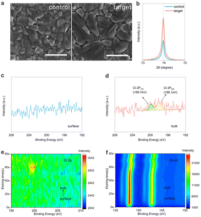
The target samples were prepared by incorporating PbCl2 at a concentration of 10%, as detailed in the Experimental section of the ESI.† Perovskite films and devices without PbCl2 incorporation were designated as the control samples. The surface morphology of the perovskite films was analyzed using scanning electron microscopy (SEM). As shown in Fig. 1a, both the control and target perovskite films exhibit uniform morphology and similar compact textures, with no observable pinholes. The target perovskite film shows a larger average grain size compared to the control, which reduces grain boundaries and defects. To determine the location of the Cl element, we first performed XRD (Fig. S1, ESI†) and XPS analyses on the control and target perovskite films for comparison. The enlarged view of the XRD patterns for all the samples at 13.9° is shown in Fig. 1b. No shifting of the peak position was observed, meaning that the surface of the final films is FAPbI3. At the same time, the XPS analysis did not detect any Cl element on the surface of the target film either (Fig. 1c). However, the intensity of the Cl peaks at 199.7 eV for Cl 2p1/2 and 198.1 eV for Cl 2p3/2 is shown in the bulk of the target film (Fig. 1d). To further confirm the presence of Cl within the bulk of the perovskite film, XPS measurements were conducted at different depths on the prepared target FAPbI3 (Fig. 1e and f). Throughout the etching process from 0 s to 50 s, no Cl signal was detected in FAPbI3, and the Pb peak remained unchanged. This suggests that the perovskite film within the etching depth from 0 s to 50 s is composed of FAPbI3. After 50 s of etching time, the Cl signal began to appear. As shown in Fig. S2 (ESI†), the Cl distribution in the bulk of the target film was observed at etching times from 45 s to 70 s. It can be observed that the Cl signal is detected starting at 50 s and disappears at 65 s. As the etching time increases, the Cl 2p peak shifts towards a higher binding energy. The Pb 4f peaks shifted gradually towards higher binding energy starting at 50 s. The peak shifting of Pb and Cl was ascribed to the introduction of Cl into the FAPI3 lattice, which resulted in the improvement of chemical bonding.23 At an etching time of 65 s, the Sn signal appeared (Fig. S3, ESI†), while the Pb and Cl signals began to disappear. The XRD results of the vapor–solid reaction at 3 min, 8 min, 15 min and 30 min (target film) are shown in Fig. S4 (ESI†). As the reaction proceeds, the perovskite characteristic peaks gradually shift toward 14° of controlled FAPbI3. The shift of the characteristic peaks indicates that substitution has occurred between I and Cl. This suggests the formation of an FAPbIxCl3−x layer between SnO2 and FAPbI3. With increasing etching time, the peaks of Pb 4f and Cl 2p shifted towards higher energy gradually. It was indicated that as the film depth increases, the content of Cl gradually increases. This leads to the formation of a gradient distribution of FAPbIxCl3−x.
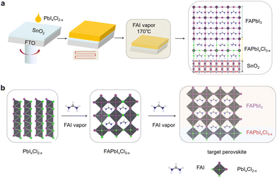
The vapor–solid reaction was employed to prepare FAPbI3. In the reaction process the coherent interface layer FAPbIxCl3−x was generated simultaneously. As shown in Fig. S5 (ESI†), the characteristic peaks of PbI2/PbCl2 remained consistent with PbI2. The 12.65° of PbI2/PbCl2 exhibited a shift compared to 12.6° of pure PbI2. This indicates that the PbI2/PbCl2 forms a pure compound, which was labelled as PbIxCl2−x in the subsequent discussion. Fig. 2a depicts the schematic diagram of the perovskite film preparation process. The PbIxCl2−x was spin-coated onto the SnO2 substrate. After annealing at 70 °C, the PbIxCl2−x film was placed in an FAI vapor environment at 170 °C for reaction. The target perovskite films FAPbI3/FAPbIxCl3−x can be obtained through a single-step vapor–solid reaction. Fig. 2b illustrates the possible evolution of the nucleation and crystallization processes of FAPbI3 perovskite films with or without PbCl2. PbI2 and PbCl2 are mixed in a certain ratio to form PbIxCl2−x. During the reaction of PbIxCl2−x film with FAI vapor, the FAPbIxCl3−x was formed. With the vapor–solid reaction proceeding, due to the Cl having much weaker bond affinity to Pb than I in the lattice under the 170 °C reaction temperature, the I ion and Cl ion exchanged gradually and the Cl ion sublimates in the form of FACl.23 By controlling the reaction time to 20 minutes, the FAPbIxCl3−x in the buried layer had not yet undergone complete substitution. The FAPbI3/FAPbIxCl3−x film was obtained simultaneously through a single vapor–solid reaction process. Not only was the dissolution issue that often arises when spin-coating the perovskite precursor eliminated, but also the buried layer of FAPbIxCl3−x and FAPbI3 exhibits perfect lattice matching. It is important to note that further research is needed to better understand the specific reaction time and the corresponding thickness of the FAPbIxCl3−x layer.
 | ||
| Fig. 2 Schematic diagram of (a) perovskite films prepared with or without PbCl2 and (b) the possible phase evolution of the nucleation and crystallization of the target FAPbI3. | ||
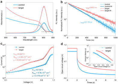
It has been reported that interface Cl atoms enhance the binding energy at the perovskite/ETL interface and promote strong electron coupling. Due to the high formation energy of Pb–Cl anti-sites, the formation of deep-level defects is suppressed, resulting in a lower density of interface trap states.26 The optical properties of both the control and target perovskite films were further explored by using ultraviolet-visible (UV-Vis) absorption and photoluminescence (PL) spectra. As shown in Fig. 3a, the absorption edges of both perovskite films are all ∼810 nm, showing excellent absorption ability. Compared to the control film, the target film exhibited a higher light absorption. This improved absorbance stems from the presence of the buried layer FAPbIxCl3−x. The FAPbIxCl3−x improved the film quality with increased grain size and crystallization, which would suppress the non-radiative recombination caused. It was indicated that the buried interface promoted the extraction and transportation of the carriers.27 The steady-state PL intensity of the target film is an order of magnitude higher than that of the control film, indicating that the formation of FAPbIxCl3−x could effectively reduce the trap density, thus minimizing the non-radiative recombination in perovskite films. Time-resolved photoluminescence (TRPL) measurements were conducted to study the carrier transport and recombination in the perovskite layer. As shown in Fig. 3b, the recombination in TRPL was dominated by second-order trap-assisted recombination. The fitted lifetime of the target film is five times longer than that of the control film (Table S1, ESI†). This substantial increase in carrier lifetime suggests a lower non-radiative recombination, which is attributed to the reduced density of trap states in the target film. Therefore, space-charge-limited current (SCLC) measurement was employed to investigate the trap density (Ntrap) of perovskite films (Fig. 3c). The dark J–V curves were measured from an electron-injecting device. Fig. 3c describes the dark J–V curves of devices based on the control and target film, respectively. The voltage (VTFL) which marked the transition from the ohmic region to the trap-filled limit (TFL) region is used to calculate the trap state density by eqn (S1) (ESI†). From the J–V curves, it can be seen that the VTFL of the control device and target devices is 0.735 V and 0.627 V, respectively. The corresponding trap state density decreased from 5.76 × 1015 cm−3 of the control film to 4.92 × 1015 cm−3 of the target film, which was consistent with the results of TRPL measurement. The low trap state density of perovskite film might associate with the enhanced VOC of the corresponding devices. The intrinsic mobility distribution, estimated by SCLC, is shown in Fig. 3c. It increased from 0.179 cm2 V−1 s−1 for the control film to 0.243 cm2 V−1 s−1 for the target film. The VOC decay is one of the effective methods to analyze the electron recombination process in the anode and perovskite film. Fig. 3d shows the VOC decay curves of PSCs based on the control film and target film, respectively. Three electron transport processes in different voltage regions explained the decay curves effectively. The exponential increase in the voltage region reflects internal trapping and de-trapping of electrons in bulk perovskite materials, which is the critical consideration of the obtained FAPbI3 layer with a different reaction process. The electron lifetime can be calculated through eqn (S2) (ESI†). The PSCs based on the target had a much longer τn than that of the control. For example, at the voltage of 0.3 V, the τn are 0.27 s and 1.22 s of PSCs based on the control and target, respectively. The FAPbIxCl3−x would increase the electron lifetime and reduce the charge recombination rate in the perovskite layer.
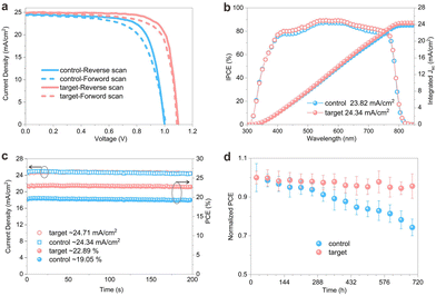
As expected from the defect concentration and carrier lifetime analysis of the perovskite films formed under each condition, the average power conversion efficiency (PCEavg) of the target devices was significantly higher than that of the control devices. The PCEavg of the target and control was 22.22% and 18.61%, respectively. The overall improvement in the target devices is primarily attributed to the enhancement of the VOC and FF. The champion device offers a high PCE of 22.89% for the reverse scan (JSC of 24.89 mA cm−2, a VOC of 1.10 V, and an FF of 79.8%) and a PCE of 22.03% for the forward scan (JSC of 24.77 mA cm−2, a VOC of 1.09 V and an FF of 77.6%), showing a negligible hysteresis of 3.1% compared with the control device of 19.05% for the reverse scan and 17.65% for the forward scan, as shown in Fig. 4a and Table S2 (ESI†). The incident photon-to-current efficiencies (IPCEs) of both the control and target devices were measured, and the integrated currents correspond well with the JSC values obtained from the J–V curves (Fig. 4b). A stabilized PCE of 22.89% for the target PSC is achieved after 200 seconds of continuous maximum power point tracking (MPPT), as shown in Fig. 4c, while the control device shows a considerably lower stabilized output of 19.05%. As shown in Fig. 4d, the unencapsulated target PSC retained 90.0% of its initial efficiency after 30 days under continuous one-sun illumination in the N2 environment. In contrast, the control device degraded to 74.0% of its initial efficiency.
In summary, this study presents a vapor–solid reaction method for preparing FAPbI3 perovskite, which simultaneously forms a coherent interface FAPbIxCl3−x passivization layer at the buried interface. The FAPbIxCl3−x shows excellent lattice matching with FAPbI3, effectively reducing interface charge recombination and enhancing charge transport. Furthermore, the chlorine atoms at the FAPbIxCl3−x film strengthen the binding energy between the perovskite and the ETL, suppressing anti-site defects and lowering the density of interface trap states. This method also avoids the dissolution of the passivization layer at the buried interface during perovskite spin-coating. In conclusion, the FAPbI3 films with the coherent interface layer FAPbIxCl3−x are simultaneously prepared using a single-step vapor–solid reaction. As a result, the VOC was increased from 1.01 V to 1.10 V, with the PCE improved from 19.05% to 22.89%.
This work was supported by the Natural Science Foundation of Hebei Province (F2023208017 and A2021208015).
Data availability
The authors confirm that the data supporting the findings of this study are available within the article.Conflicts of interest
There are no conflicts to declare.Notes and references
- https://www.nrel.gov/pv/cell-efficiency.html .
- Y. Zhang, R. Yu, M. Li, Z. He, Y. Dong, Z. Xu, R. Wang, Z. Ma and Z. Tan, Adv. Mater., 2024, 36, e2310203 CrossRef PubMed.
- K. Wang, L. Zheng, Y. Hou, A. Nozariasbmarz, B. Poudel, J. Yoon, T. Ye, D. Yang, A. V. Pogrebnyakov and V. Gopalan, Joule, 2022, 6, 756–771 CrossRef.
- C. Luo, G. Zheng, F. Gao, X. Wang, C. Zhan, X. Gao and Q. Zhao, Nat. Photonics, 2023, 17, 856–864 CrossRef.
- G. Liu, X. Jiang, W. Feng, G. Yang, X. Chen, Z. Ning and W. Q. Wu, Angew. Chem., Int. Ed., 2023, 62, e202305551 CrossRef PubMed.
- C. Wang, J. Wu, S. Wang, Z. Yan, X. Liu, G. Li, L. Chen, S. Zhu, W. Sun and Z. Lan, Solar RRL, 2022, 6, 2100995 CrossRef.
- C. Zhao, Q. Zhang, Y. Lyu, J. Liu, F. Shen, H. Liu, H. Kong, H. Han, A. Krishna and J. Xu, Adv. Funct. Mater., 2024, 34, 2404099 CrossRef.
- H. Han, J. Xu, H. Liu, Y. Fu, C. Zhao, R. Shi, H. Zhang and J. Yao, ACS Energy Lett., 2023, 8, 4608–4616 CrossRef.
- Z. Li, Y. Ren, W. Chen, T. Wei, L. Mo, Y. Huang, H. Zhang, G. Cao and L. Hu, Renewables, 2023, 1, 572–581 CrossRef.
- L. Zhang, L. Mei, K. Wang, Y. Lv, S. Zhang, Y. Lian, X. Liu, Z. Ma, G. Xiao and Q. Liu, Nano-Micro Lett., 2023, 15, 177 CrossRef.
- F. Cao, Z. Zhu, C. Zhang, P. Chen, S. Wang, A. Tong, R. He, Y. Wang, W. Sun and Y. Li, Small, 2023, 19, 2207784 CrossRef.
- C. Zhao, H. Zhang, A. Krishna, J. Xu and J. Yao, Adv. Opt. Mater., 2024, 12, 2301949 CrossRef.
- C. Zhao, H. Zhang, M. Almalki, J. Xu, A. Krishna, F. T. Eickemeyer, J. Gao, Y. M. Wu, S. M. Zakeeruddin and J. Chu, Adv. Mater., 2023, 35, 2211619 CrossRef.
- H. Li, C. Zhang, C. Gong, D. Zhang, H. Zhang, Q. Zhuang, X. Yu, S. Gong, X. Chen, J. Yang, X. Li, R. Li, J. Li, J. Zhou, H. Yang, Q. Lin, J. Chu, M. Grätzel, J. Chen and Z. Zang, Nat. Energy, 2023, 8, 946–955 CrossRef.
- S. Zhang, F. Ye, X. Wang, R. Chen, H. Zhang, L. Zhan, X. Jiang, Y. Li, X. Ji and S. Liu, Science, 2023, 380, 404–409 CrossRef PubMed.
- C. Liu, Y. Yang, H. Chen, J. Xu, A. Liu, A. S. Bati, H. Zhu, L. Grater, S. S. Hadke and C. Huang, Science, 2023, 382, 810–815 CrossRef PubMed.
- J. Zhang, B. Yu, Y. Sun and H. Yu, Adv. Energy Mater., 2023, 13, 2300382 CrossRef.
- Y. Zhou, Z. Wang, J. Jin, X. Zhang, J. Zou, F. Yao, Z. Zhu, X. Cui, D. Zhang and Y. Yu, Angew. Chem., Int. Ed., 2023, 62, e202300759 CrossRef PubMed.
- Y. W. Jang, S. Lee, K. M. Yeom, K. Jeong, K. Choi, M. Choi and J. H. Noh, Nat. Energy, 2021, 6, 63–71 CrossRef.
- Q. Chen, J. Wu, X. Liu, Y. Du, C. Deng, X. Chen, L. Sun, L. Tan, W. Sun and Z. Lan, ACS Appl. Mater. Interfaces, 2024, 16, 8949–8959 CrossRef.
- H. Min, D. Y. Lee, J. Kim, G. Kim, K. S. Lee, J. Kim, M. J. Paik, Y. K. Kim, K. S. Kim and M. G. Kim, Nature, 2021, 598, 444–450 CrossRef PubMed.
- C. Duan, J. Zhong, S. Hu, Y. Dou, J. Lu, Y. B. Cheng and Z. Ku, Adv. Funct. Mater., 2024, 34, 2313435 CrossRef.
- J. Chen, J. Xu, C. Zhao, B. Zhang, X. Liu, S. Dai and J. Yao, ACS Appl. Mater. Interfaces, 2019, 11, 4597–4606 CrossRef PubMed.
- Y. Ren, H. Fu, Y. Li, Z. Li, C. Li and X. An, Chem. Commun., 2024, 60, 2938–2941 RSC.
- Y. Ren, J. Chen, D. Ji, Y. Sun and C. Li, Chem. Eng. J., 2020, 384, 123273 CrossRef.
- E. Mosconi, E. Ronca and F. De Angelis, J. Phys. Chem. Lett., 2014, 5, 2619–2625 CrossRef PubMed.
- C. Ge, L. Xie, J. Yang, K. Wei, T. Wu, L. Wang, L. Sun, J. Zhang and Y. Hua, Adv. Funct. Mater., 2024, 34, 2313688 CrossRef.
Footnote |
| † Electronic supplementary information (ESI) available. See DOI: https://doi.org/10.1039/d4cc06599a |
| This journal is © The Royal Society of Chemistry 2025 |


