
 Open Access Article
 This Open Access Article is licensed under a
 Creative Commons Attribution 3.0 Unported Licence
Structure–property relationships of Group IV (Si–Ge–Sn) semiconductor nanocrystals and nanosheets – current understanding and status
Jeremy B.
Essner†
 ,
Maharram
Jabrayilov†
,
Andrew D.
Tan
,
Abhishek S.
Chaudhari
,
Abhijit
Bera
,
Brodrick J.
Sevart
and
Matthew G.
Panthani
*
,
Maharram
Jabrayilov†
,
Andrew D.
Tan
,
Abhishek S.
Chaudhari
,
Abhijit
Bera
,
Brodrick J.
Sevart
and
Matthew G.
Panthani
*
Iowa State University, 618 Bissell Road, 2037 Sweeney Hall, Ames, Iowa 50011, USA. E-mail: panthani@iastate.edu; Tel: +1-515-294-1736
First published on 9th May 2025
Abstract
Group IV semiconductor nanomaterials, including silicon nanocrystals and more recently nanosheets, are emerging as promising candidates for next-generation optoelectronic applications due to their tunable room-temperature photoluminescence and compatibility with CMOS technologies. However, the intrinsic indirect bandgaps of Group IV seminconductors remains a key limitation. Here, we highlight our group’s contributions toward understanding structure–property relationships in solution-processable Group IV semiconductor nanocrystals and nanosheets - specifically, understanding how their structure, surface chemistry, and chemical composition influence affect properties such as bandgap.
1 Introduction
Nanostructured Group IV semiconductors comprised of Group IVA (or Group 14) elements have emerged as promising materials for next-generation optoelectronic devices.1–4 Group IV semiconductors are relatively abundant, inexpensive, and non-toxic; they also offer a key advantage over other prospective materials such as IIIA–VA (e.g., GaAs, GaN, InAs) and (metal halide) perovskites in that they are compatible with the CMOS process, enabling seamless integration into the existing microelectronic infrastructure.5,6Table 1 summarizes the key advantages of Group IV semiconductors over other semiconductor classes. The primary challenge in using conventional Group IV semiconductors for many applications is their indirect bandgaps,7 which make them poor light emitters, even at cryogenic temperatures.8 This fundamental challenge can potentially be overcome by confining the physical dimensions of these materials to the nanoscale in one, two, or three dimensions to create 2D nanosheets (NSs), 1D nanowires, 0D nanocrystals (NCs). Indeed, nanostructuring has been shown to dramatically enhance photoluminescence (PL) in Group IV nanostructures.9–11 Another approach to improving light emission has been the synthesis of Group IV nanoalloys (e.g., Si1−xGex, Ge1−xSnx, Si1−xSnx, or Si1−x−yGexSny),12–18 in which the random distribution of the Group IV elements within the alloy may break the translational symmetry that gives rise to the indirect bandgaps of bulk Si and Ge.19| Property | Group IV | Group III–V/II–VI |
|---|---|---|
| CMOS compatibility | Excellent | Requires heterointegration |
| Commercial viability | High (low cost, abundant) | Low (high cost, scarce) |
| PL quantum yield (ΦPL) | Improved with nanostructuring and alloying | Requires complex production for high values |
| Band structure engineering | Alloying or strain affords visible to MIR tunabilty | Requires elaborate heterostructures; restricted to NIR |
| Environmental impact | Minimal to none (nontoxic, sustainable) | High (toxic) |
Many prior efforts have targeted the issue of band structure in Group IV semiconductor nanomaterials; however – with the exception of Si-based nanomaterials – they are often characterized by relatively weak or non-existent light emission (ΦPL often below 10%) due to (i) poorly understood synthesis–structure relationships, (ii) loosely established, and sometimes conflicting, structure–property relationships, including the role that surface states/chemistry play, and (iii) elusive origins of light emission in as-prepared materials. Thus, deeper understanding of these nanomaterials’ structure, chemistry, and properties is necessary to achieve commercial viability.
Here, we highlight our contributions to the broader understanding of structure–property relationships in Group IV semiconductor nanomaterials, with a particular focus on SiNCs and SiNSs. Specifically, we summarize how synthetic conditions, structure, morphology, surface chemistry, and composition influence the optoelectronic properties, namely the band structure and PL (Scheme 1). Lastly, we conclude with broad challenges for these materials and suggest potential paths forward.
 | ||
| Scheme 1 Factors influencing electronic properties in solution-processable Group IV semiconductor nanomaterials towards band structure engineering. | ||
2 Nanocrystals
Group IV semiconductor NCs have been investigated for many decades due to their potential use in solar cells,20 light emitting diodes,11 and photodetectors.21 The interest in the field began in the early 1990s with the synthesis of 3 nm silicon crystallites via electrochemical etching of silicon wafers, resulting in red emission,22 followed by the synthesis of highly luminescent (ΦPL of 5–20%) hydride- and alkoxide-terminated SiNCs in the 2000s;23 these NCs also displayed electrogenerated chemiluminescence.24 From 2005 to present, our group has made notable contributions to understanding structure–property relationships of Group IV NCs, as outlined below.2.1 Silicon nanocrystals
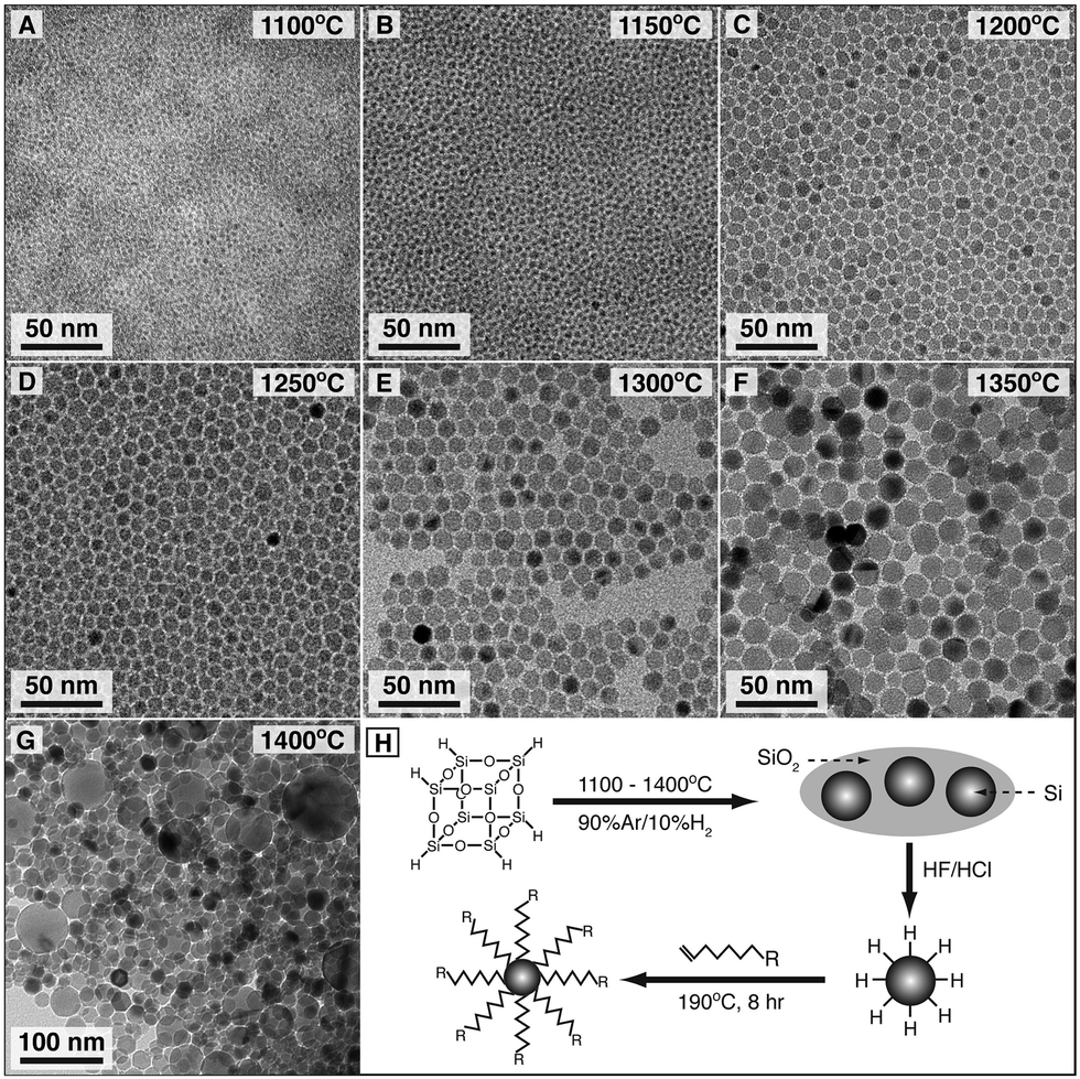 | ||
| Fig. 1 (a)–(g) TEM of alkyl-terminated SiNCs generated through HSQ decomposition at the indicated temperatures, followed by HF etching and thermal hydrosilylation with terminal alkenes, as schematically shown in panel (h). (Reproduced with permission from ref. 25 Copyright 2012 American Chemical Society). | ||
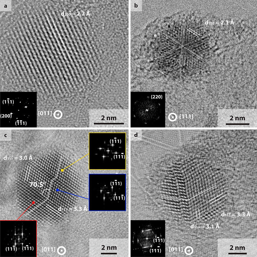 | ||
| Fig. 2 The defect free (a) and twinned lattice structure (b)–(d) of SiNCs acquired with bright-field STEM. The alkyl-passivated SiNCs were demonstrated in panels (a), (c) and (d) whereas hydride-terminated silicon nanocrystal was shown in panel (b) (Reprinted with permission from ref. 26 Copyright 2012 American Chemical Society). | ||
![[thin space (1/6-em)]](https://www.rsc.org/images/entities/char_2009.gif) :1 ratio 1-DD:1-OD) enhanced the ligand surface coverage and colloidal stability of SiNCs, especially for NCs greater than approximately 8 nm.25 Additionally, rigorous purification of the passivated NCs is key for removing impurities, such as residual ligand, that can interfere with (optical) characterization. Towards this, we found that multiple solvent/antisolvent washing/precipitation cycles were highly effective for removing impurities and obtaining clean, optically transparent SiNC dispersions.25 Further, we also demonstrated that hydrosilylation of SiNC surfaces can be facilitated by either ω-ester-terminated (alkene-COOR) or ω-acid-terminated alkenes (alkene-COOH) at room temperature,27 where the bifunctional ligands catalyze the hydrosilylation process by the nucleophilic carbonyl group of the ester (or acid) enhancing coordination with the oxophilic silicon surface and thereby the reactivity of silicon–hydrogen (Si–H) species toward the terminal alkenes, as shown in Fig. 3.
:1 ratio 1-DD:1-OD) enhanced the ligand surface coverage and colloidal stability of SiNCs, especially for NCs greater than approximately 8 nm.25 Additionally, rigorous purification of the passivated NCs is key for removing impurities, such as residual ligand, that can interfere with (optical) characterization. Towards this, we found that multiple solvent/antisolvent washing/precipitation cycles were highly effective for removing impurities and obtaining clean, optically transparent SiNC dispersions.25 Further, we also demonstrated that hydrosilylation of SiNC surfaces can be facilitated by either ω-ester-terminated (alkene-COOR) or ω-acid-terminated alkenes (alkene-COOH) at room temperature,27 where the bifunctional ligands catalyze the hydrosilylation process by the nucleophilic carbonyl group of the ester (or acid) enhancing coordination with the oxophilic silicon surface and thereby the reactivity of silicon–hydrogen (Si–H) species toward the terminal alkenes, as shown in Fig. 3.
 | ||
| Fig. 3 Mechanistic illustration of room temperature hydrosylilation of silicon nanocrystals in the presence of methyl 10-undecenoate. The methyl 10-undecenoate was demonstrated in its resonance structure to highlight electrostatic interaction with the hydride-terminated silicon nanocrystal surface. (Reproduced with permission from ref. 27 Copyright 2013 American Chemical Society). | ||
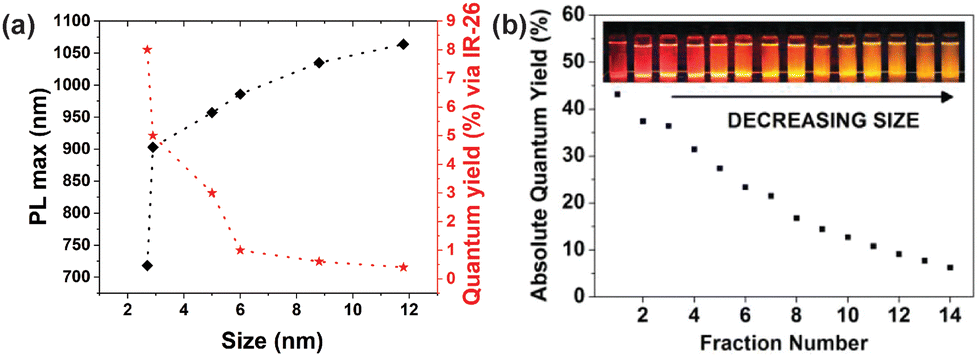 | ||
| Fig. 4 The size-dependent photoluminescent properties of SiNCs. (a) The relationship between PL peak maximum and relative ΦPL as a function of SiNC size. The ΦPL values were assessed vs. the infrared-emitting, reference fluorophore IR-26. (b) Size-dependent absolute ΦPL values of SiNCs obtained via size-selective precipitation. (Panels (a) and (b) were adapted with permission from ref. 25,46, respectively. Copyright 2012 American Chemical Society). | ||
| Precursor | Ligand | Size (nm) | Peak PL (eV) | Φ PL (%) | Ref. |
|---|---|---|---|---|---|
| HSQ | 1-DD, 1-OD | 1.0–12.0 | 1.1–1.7 | 0.4–8.0 | 25 |
| 10-UDA, M-10-UD, E-10-UD | 2.3 | 1.9 | 7.0 | 27 | |
| 1-H, 1-DD, M-10-UD | 3.0–5.0 | 1.4–1.8 | 30–70 | 10 | |
| 1-P, 1-DD, 1-DDY, M-10-UD | 3.0–8.2 | 1.8 | 62 | 48 | |
| 1-D | 2.7–3.9 | 1.7 | 38 | 49 | |
| SiO | 1-D | 3.5–4.0 | 1.5 | 4.0–16 | 30 |
| 1-DD | 2.9 | 1.5 | — | 29 | |
| HSQ polymer | 1-DD | 3.0–6.7 | 1.3–1.7 | — | 50 |
| 1-DD | 3.9–6.4 | 1.3–1.5 | 19–41 | 51 | |
| 1-OD | 4.9 | 3.0 | 2.5–21 | 52 | |
| 1-O, 1-D, 1-OD | 2.1–3.6 | 1.5–1.7 | 44–56 | 35 | |
| M-10-UD | 4–5 | 1.5 | 20–40 | 53 | |
| 10-UDA | 1.8 | 1.7 | 22 | 54 |
Another viable avenue for tuning the electronic properties of SiNCs is through alloying with germanium to yield Si1−xGex NCs. Although our group has yet to publish work in this area, such alloys are predicted to have size-, shape-, and composition-dependent electronic properties13,55 and can be synthesized and surface terminated via similar routes to SiNCs,56–62 with size and compositional tunability arising from varied Si:Ge ratios59 and reaction temperatures.58,59 The as-synthesized hydrogen-terminated Si1−xGex NCs are reported to have a PL peak maximum around 1.55 eV, with air oxidation blueshifting the PL energy about 0.1 eV due to a decrease in size,56,57 while both blue PL (3.45 eV) and infrared PL (1.3 eV to 1.6 eV) have been observed, depending on the hydrosilylation reaction or ligand.56,58,60–62
2.2 Germanium nanocrystals
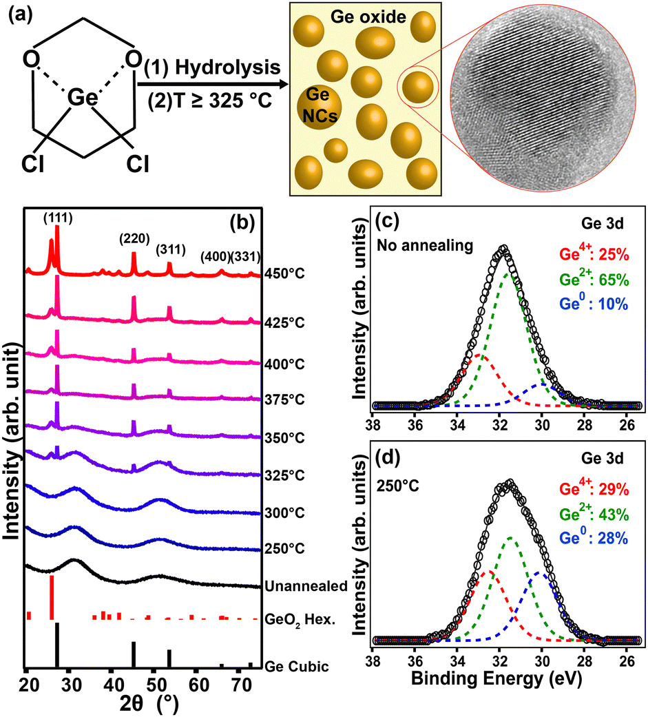 | ||
| Fig. 5 (a) Schematic illustration of GeNCs synthesis via the thermally-induced disproportionation of hydrolyzed GeCl2·dioxane. (b) XRD patterns of hydrolyzed GeCl2·dioxane processed at different temperatures under N2 flow. XPS of (c) unannealed and (d) annealed (250 °C) hydrolyzed GeCl2·dioxane precursor indicating the formation of nanocrystals and amorphous GeO2. (Reproduced from ref. 67 with permission from the Royal Society of Chemistry). | ||
Similar to alloyed Si1−xGex NCs, alloying of tin with germanium is a viable route for electronic property modulation. Again, while our group has yet to contribute to this area, Ge1−xSnx NCs alloys are predicted to have an indirect-to-direct bandgap transition with increasing Sn content,12 with the simulated electronic properties of tetrahedrally coordinated NC alloys being dependent upon size, shape, and composition.12,86,87 In general, Ge1−xSnx alloyed NCs are typically synthesized through convective or microwave heating of Ge and Sn halides (or Sn amides) in alkylamines, assisted by a (strong) reducing agent, such as n-butyllithium (n-BuLi), leading to alkylamine-terminated NCs, with the synthetic conditions impacting the size and composition.88–91 Through these approaches, size- (1–20 nm) and composition- (up to 95% Sn) dependent electronic properties have been demonstrated, with increasing Sn content redshifting the absorbance onset and PL from the visible (2 eV) to the infrared (<1 eV),86,87,89,91 while still maintaining the diamond cubic lattice.90
3 Two-dimensional nanosheets
In recent years, solution-processable methods, such as topotactic deintercalation of Zintl phase precursors (Fig. 6(a)),92 have arisen as promising approaches towards free-standing Group IV NSs, as these approaches boast (i) less demanding and more cost-effective experimental conditions, (ii) higher synthetic throughput and yields, and (iii) improved chemical stability through, often in situ, surface termination (with hydrogen),93 compared to bottom-up approaches such as epitaxial growth. Furthermore, this surface termination results in an opening of the bandgap,9,94–97 with the Group IV NSs theoretically predicted to be (quasi-) direct bandgap semiconductors with excitonic optical absorption, sizeable bandgaps (silicane – 3.60 eV, germanane – 2.21 eV, and stanane – 1.35 eV), and strongly bound excitons, with binding energies of 0.40 to 1.07 eV, 0.33 to 0.92 eV, and 0.20 eV, respectively.98,99 Additionally, the bandgaps of silicane and germanane have been computationally shown to be marginally affected by external electric fields, with a non-zero gap still existing at high field strength.100 Furthermore, promising transport properties,101,102 such as high carrier mobilities,103,104 have been demonstrated for silicane and germanane. These properties and potential electronic structure tunability make Group IV nanosheets enticing prospects for low energy, next-generation photonics, optoelectronics, or optical computing devices, with potential for integration into current silicon-based manufacturing infrastructure.105 Indeed, Group IV NSs have recently shown promise in photosensitive devices.106–110 The following sections highlight our contributions to structure–property relations in 2D Group IV nanosheets, with an emphasis on 2D Si and the overall focus on nanosheets derived from the topotactic deintercalation of Zintl phase compounds. | ||
| Fig. 6 Silicon nanosheets (SiNSs) synthesized by deintercalation of Ca2+ from calcium disilicide (CaSi2); the CaSi2 was prepared via both elemental melt (EM) and hydride synthesis (HS) approaches. (a) Schematic illustration of EM and HS approaches for the formation of Zintl phase CaSi2 precursor. (b) Powder X-ray diffraction patterns of EM- and HS-CaSi2. The 6R phase CaSi2 reference pattern is shown in blue. (c) AI-spXRD of EM- and HS-SiNSs. SEM images of SiNSs derived from (d) EM and (e) HS approaches. (Modified with permission from ref. 111 Copyright 2023 American Chemical Society). | ||
3.1 Silicon nanosheets
Precise control over the CaSi2 polymorphism is expected to impact their properties.129,130 Yao et al. very recently predicted that the stacking order of the CaSi2 precursor should strongly influence the electronic properties of SiNSs. SiNSs derived from 1H and 6R polytypes are expected to exhibit interlayer charge transfer while those derived from the 3R polytype is not expected to exhibit interlayer charge transfer.131 Further, it is important to have phase-pure Zintl phase precursors in order to properly draw conclusions regarding structure–property relationships.9 While most commercial sources of CaSi2 contain CaSi, Si, or FeSi2 impurities, washing the precursor with a strong base is reported to remove bulk Si impurities;116 however, FeSi2 has proved difficult to remove.132 Given these impurity issues, we investigated two different synthetic approaches for the preparation of high-purity 6R-CaSi2, specifically, (i) the conventional elemental melt (EM) method and (ii) a less explored hydride synthesis (HS; Fig. 6).111 The primary advantage of the latter is the reaction occurs at temperatures below the peritectic decomposition of CaSi2. Although we produced high-purity CaSi2 through both approaches, as confirmed by pXRD (Fig. 6(b)), the EM approach resulted in preferential, isotropic growth of CaSi2 along the c-axis while the HS method yielded more uniform CaSi2 crystals with shorter lateral dimensions (see (00 12) reflection in Fig. 6(b)). We found that these features translated to the SiNSs upon deintercalation, with those resulting from the EM method having significantly larger lateral dimensions than the SiNSs resulting from the HS method (Fig. 6(d) and (e)). Our conclusion was further supported by azimuthally integrated synchrotron powder X-ray diffraction (AI-spXRD) measurements taken at Argonne National Lab (Fig. 6(c)), which displayed a more intense (006) reflection for the EM-SiNSs compared to the HS-SiNSs.
More recently, we demonstrated that the siloxane (Si–O–Si) content previously observed in SiNSs primarily originates from oxidation of silicon monolayers by dissolved oxygen in the deintercalant solution (i.e., HCl), although, exposure to oxygen at any point after deintercalation will also contribute to (further) oxidation of the backbone, through oxygen insertion between Si–Si bonds.121 Literature has demonstrated that these siloxanes (and other silicon oxides) can be removed through HF treatment,117 however, this may be problematic depending on the desired application, as the etching of the inserted oxygen from the Si framework will effectively cleave the SiNSs, reducing their lateral dimensions. Furthermore, our results suggest that oxidation of the Si framework leads to further buckling of the monolayers which pushes the layers apart, evident by an increase in interlayer spacing with increasing oxygen exposure.121
Lastly, we investigated the structural impact on the SiNSs upon annealing for 10 min at temperatures between 100 and 400 °C (Fig. 7(a) and 8(b)).96 Both our pair distribution function (PDF) and spXRD results indicated minimal degradation of the silicon monolayers up to 300 °C, after which, the monolayers showed increasing amorphization with higher annealing temperature; that is, the SiNSs began to crosslink via amorphous Si–Si bond formation resulting in a coalesced amorphous silicon structure, evidenced by the smoothing of PDF peaks and broadening of peaks in spXRD due to increased disorder as annealing temperature increased.
 | ||
| Fig. 7 Impact on the structure, chemistry, and optical properties of SiNSs upon annealing. (a) PDF of SiNSs annealed at various temperatures. Inset shows agreement of simulated and experimental results for SiNSs annealed at 425 °C. (b) AI-spXRD mapped over temperature showing amorphization starting around 300 °C. (c) FTIR of annealed SiNSs indicating loss of surface groups as annealing temperature increases. (d) Time-resolved and steady-state (inset) PL of annealed SiNSs. (e) EPR response of annealed SiNSs indicating generation of dangling bonds at higher annealing temperatures. Inset shows relative integrated EPR absorbance. (Reproduced with permission from ref. 96 Copyright 2021 American Chemical Society). | ||
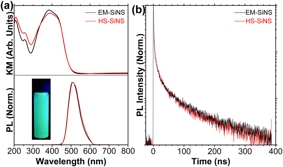 | ||
| Fig. 8 Measurements of optical properties of EM and HS SiNSs. (a) Kubelka–Munk transformation of diffuse reflectance (top), used as a representative absorbance spectra of the SiNSs. Steady-state PL emission spectra of SiNSs excited at 370 nm (bottom). (b) Time-resolved PL of SiNSs excited at a wavelength of 359 nm and measured at 510 nm. (Modified with permissions from ref. 111 Copyright 2023 American Chemical Society). | ||
As SiNSs are primarily hydrogen terminated when prepared with cold (mineral) acids,9,96,97,111,121 the surface chemistry can be further altered through surface modifying, nucleophilic substitution or addition reactions widely reported for silicon surfaces,95,137 such as hydrosilylation,138–140 amination,106 or Grignard strategies,141 affording termination with various organic moieties tethered to the SiNSs via Si–C–R, Si–N–R, or Si–O–R linkages. Furthermore, simultaneous decalciation and organic termination has been reported.142,143
Experimentally, the bandgap energy (Eg) of (mostly) hydrogen-terminated SiNSs has been reported to range from 2.79 to 2.20 eV with peak PL observed between approximately 440 and 560 nm,151–154 and ΦPL values of 9 to 10%;152,155 our results are consistent with the above ranges, with peak PL mainly centered around 2.48 eV (500 nm)—although we have observed a range of 2.53 to 2.33 eV (490 to 530 nm)—and ΦPL values of approximately 9% (Fig. 8(a); lower panel).9,111,121 Our steady-state PL results, in combination with time-resolved PL suggest direct-like bandgap behaviour, consistent with our DFT predictions for H-SiNSs,9,96,97 with our SiNSs exhibiting short carrier lifetimes (Fig. 8(b)).111 Additionally, our PL results (Fig. 8(a); lower panel) display narrower full-width at half-maxima than other nano-Si forms like nanocrystals or porous Si.9,96,97,111 Our results also demonstrated that the macroscopic properties of phase-pure CaSi2 and resultant SiNSs have minimal to no impact on the observed optical properties (Fig. 8).111
As our freshly prepared SiNSs typically present with some degree of oxidation,9,96 in the form of siloxanes,121 and our previous band structure simulations predicted that oxidized SiNSs are direct bandgap semiconductors,96 one potential origin of the previously observed PL is oxidation of the Si framework. Indeed, our recent study demonstrated that employing rigorously degassed HCl as the deintercalant yields essentially non-oxidized SiNSs (Fig. 9) with the lowest siloxane (Si–O–Si) content observed to date (without a post-deintercalation HF treatment).121 Our SiNSs prepared through this approach were effectively non-emissive, with peak PL centered near 610 nm and ΦPL values an order of magnitude lower than previously reported values for SiNSs synthesized in air-saturated HCl (<0.6% vs. 9%). Additionally, we attributed the weak shoulder observed near 2.43 eV (510 nm) to slight oxidation (indicated by FTIR). Indeed, when we intentionally exposed the SiNSs to incrementally larger quantities of dried air (i.e., molecular oxygen), we observed increasing oxidation of the SiNSs (confirmed by FTIR; Fig. 9(b)) that was accompanied by a marked increase in the 510 nm feature and ΦPL to over 8%, consistent with our DFT predictions on oxidized SiNSs,96 after which the PL blueshifted slightly to 500 nm and the ΦPL decreased below 5% (Fig. 9(c)), which we attributed to increasing SiO2 character. We hypothesize that changes in observed PL originate from conformational alterations to the Si framework, due to oxygen insertion that further buckled the Si framework;96,121 such conformational changes (armchair vs. boat-like configuration) are predicted to shift the band structure from quasi-direct to direct.144–146 These predicted and observed electronic restructurings may arise from the laterally strained Si framework,156 as Kim et al. predicted that increasing biaxial strain induces an indirect-to-direct bandgap transition.157 We note that HF treating the SiNSs to remove these oxides has been reported to blueshift and decrease the PL, relative to the as-prepared sample.158
 | ||
| Fig. 9 (a) Schematic highlighting impacts of deintercalation of CaSi2 with degassed HCl at −35 °C and subsequent oxidation of the silicon framework with dried air. (b) FTIR of SiNSs exposed to 0.0, 1.1, or 8.4 pph O2 (relative to Si). (c) Steady-state PL spectra and associated absolute ΦPL values for SiNSs exposed to 0.0, 1.1, or 8.4 pph O2 (relative to Si). (Modified with permissions from ref. 121 Copyright 2025 Royal Society of Chemistry). | ||
Contrary to our results on intentional SiNS oxidation,121 our previous study, in which SiNSs were annealed at temperatures up to 450 °C, suggests that increasing SiNS oxidation (Fig. 7(c)) decreases PL (Fig. 7(d)).96 Specifically, for annealing temperatures up to 200 °C, we observed that the relative PL intensity only decreased marginally, while increasing the annealing temperature to 300 °C reduced the PL intensity by over half the original value and higher annealing temperatures (375 °C) leading to an effectively non-photoluminescent material (Fig. 7(d)). A key difference between our two works is that annealing of the SiNSs led to homolytic cleavage of surface groups producing Si dangling bonds (evidenced by EPR; see Fig. 7(e)) and a coalesced amorphous silicon structure that decreased the PL; the former is consistent with our own DFT predictions that Si radicals (silyl groups) introduce midgap states.96
In addition to structural changes to the Si framework impacting the electronic properties, our results demonstrate that modulating the SiNS surface chemistry leads to noteworthy changes to the band structure and bandgap.9,96,97 As previously mentioned, we predicted that SiNSs with a composition of (SiH0.7Cl0.2(OH)0.1) are a direct bandgap material with an Eg of 1.68 eV, compared to the quasi-direct H-SiNSs with direct and indirect transitions of 2.1 and 2.05 eV, respectively.97 More recently, we demonstrated that SiNSs with a nominally equivalent surface composition possess an experimentally observed bandgap of approximately 2.03 eV with a ΦPL < 0.6% while oxidized SiNSs displayed a bandgap of approximately 2.43 eV with a ΦPL > 8%.121 Additionally, our works also demonstrated that both oxidation and annealing of the SiNSs led to the loss of these surface groups via currently unknown oxidative mechanisms and homolytic bond cleavage, respectively;96,121 however, other than silyl formation upon annealing, we have yet to establish correlations between the lost surface termination and optical properties. Additionally, while we have computationally predicted the effects of chlorine (and loosely hydroxyl) termination on electronic properties,97 we (and others) have yet to experimentally explore the impacts that increased chlorine or hydroxyl content have; however, literature suggests that the hydroxyl content of the SiNS surface can be increased via water exposure.135 Lastly, we note that conflicting conclusions exist in the literature on other surface terminations (e.g., alkyl), with some reporting that formation of Si–C bonds has minimal impact on the observed PL,159 while others report both blue- and redshifts in the observed optical properties for the formation of Si–C/Si–N or Si–C bonds, respectively;106,141,142,160 our results on SiNS oxidation121 suggest that the observed blueshifts in these works may arise from oxidation of the silicon framework, as FTIR in these works indicated that oxidation of the Si framework occurred upon the ligand exchange from hydrogen to alkyl groups.
Similar to SiNCs, alloying the SiNSs with Ge is a promising approach for modulating the material's electronic properties. While our group has yet to contribute to this area, we want to highlight key works and conclusions for these Si1−xGex alloyed NSs. Layered Zintl phase CaSi2−2xGe2x (x = 0.1–0.9) has been successfully prepared and decalciated to yield Si1−xGex alloyed NSs using similar approaches to SiNSs.14,110,161 Decalciation of the CaSi2−2xGe2x Zintl phase precursors with cold HCl is reported to yield fully hydrogen-terminated Ge sites while Si atoms are fully hydroxyl terminated, except for Si1−xGex with x ≥ 0.5, where the silicon sites have mixed hydrogen and hydroxyl termination.14 Similar to SiNSs, the predicted energetically stable configuration for the deintercalated, alloyed monolayers is a buckled, armchair conformation,15 with experimental evidence suggesting this conformation is maintained for the Si1−xGex alloys upon deintercalation.14,110 Termination of the Si1−xGex alloyed NSs’ surface (e.g., hydrogen, hydroxyl) is predicted to open the bandgap, resulting in direct bandgap materials with Eg spanning the visible (2.45 eV) to near-infrared (1.53 eV) due to increasing Ge content redshifting the predicted bandgap.14,15 Consistent with predictions, increasing Ge content in the Si1−xGex alloyed NSs is reported to lead to tuneable bandgaps from the visible (2.57 eV) to the near infrared (1.53 eV);14,110 however, to the best of our knowledge, room-temperature PL has yet to be observed. Further, these materials typically present with some degree of framework oxidation,14,110 typically in the form of Si–O–Si (not Ge–O–Ge), which may play a role in the observed electronic properties, similar to our results for SiNSs.121
3.2 Germanium nanosheets
:50 for GeNSs vs. 1:6 for SiNSs).97,173 Similarly, literature suggests that minor halide termination can result when deintercalating with other halide-containing chemicals (e.g., HBr, HI, ICl).163,167 Furthermore, radical- or thermal-induced hydrogermylation or Grignard strategies can be employed to modify the surface of hydrogen-terminated GeNSs to alkyl (e.g., dodecane) termination.95,167,182 In addition to these conventional approaches, other surface termination strategies have more recently been explored to yield Ge–C or Ge–S linkages.162,183,184
We prepared methyl-terminated GeNSs using a one-step metathesis approach in which CaGe2 was simultaneously deintercalated and alkylated by methyliodide;179,180 this approach was developed by the Goldberger group,171,175 with multiple alkylhalides reported since, leading to numerous types of alkyl-terminated GeNSs.170,172,174,176–178 In this approach, smaller terminal groups generally lead to near 100% surface coverage while larger, sterically bulky groups result in mixed termination, typically consisting of the alkyl group and hydrogen.185 Given this, we chose to deintercalate CaGe2 with the shortest reported alkylhalide, methyliodide.179,180 To avoid oxidation of the GeNSs, which necessitates an HCl wash to remove the oxides, with a byproduct being chlorine termination that leads to further oxidation,175 we conducted the deintercalation of CaGe2 using a 1:30:10:60 molar ratio of CaGe2:methyliodide:water:acetonitrile,179,180 since Goldberger and coworkers reported that distilled acetonitrile with at least six equivalents of water is necessary for increased methyl coverage and improved air stability.171 We observed improved thermal stability of the methyl-terminated (CH3-) GeNSs over H-GeNSs,180 consistent with reports that the surface demethylates between 250 and 300 °C,175 compared to 200 to 250 °C for H-GeNSs.173
We observed that replacing hydrogen termination on GeNSs with alkyl (i.e., methyl) groups, via deintercalation with methyliodide instead of HCl, increased the bandgap of the CH3-GeNSs to 1.80 eV to 1.95 eV,179,180 compared to reported values of approximately 1.3 eV to 1.6 eV for H-GeNSs,154,162,168,173 a blueshift that is consistent with others’ conclusions;175,176,178 however, others have reported that H-GeNSs exhibit intense PL centered at approximately 1.35 eV (or 918 nm).154,189 Additionally, we concluded that the PL of CH3-GeNSs consists of two contributions—one from the band edge and the other from trap states—with our time-resolved measurements suggesting that the rate of trap-assisted recombination is slower than band-to-band recombination (Fig. 10).179 Conversely, Goldberger and coworkers demonstrated that the intense PL observed at 1.87 eV for CH3-GeNSs arises from local distortions of the Ge framework due to intercalated water,195 with the water-induced PL comprised of two distinct exciton populations localized at recombination centers within the intercalated water;196 thus, our previously observed PL results may originate from intercalated water. Further, the band-edge fluorescence is reported to be essentially independent of layer thickness with ΦPL = 0.2%.175 In addition to methyl termination, others have reported various effects on the observed PL for different alkyl termination, both from alkylhalide deintercalation or post-deintercalation modification,162,174,177,178,197 with ligand-bandgap trends remaining elusive. Although, Jiang et al. demonstrated that installing larger, more electronegative ligands on GeNSs (e.g., –CH3vs. –CH2OCH3) reduced Eg from 1.66 eV to 1.45 eV due to the electron-withdrawing and steric bulk of the terminal groups expanding the Ge framework.185 Further, we also demonstrated that our CH3-GeNSs display ohmic behavior that is stable at higher temperatures (280 vs. 190 °C) compared to H-SiNSs (Fig. 11).180
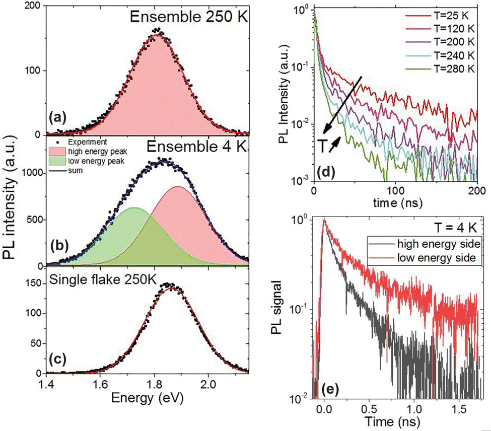 | ||
| Fig. 10 PL spectra of methyl-terminated germanane flakes (a) at 250 K ensemble, (b) at 4 K ensemble, and (c) at 250 K single flake. (d) Time-resolved PL of a CH3-GeNS film at various temperatures. (e) Time-resolved PL for a single flake of germanane at 4 K. (Modified with permission from ref. 179 Copyright 2019 AIP Publishing). http://creativecommons.org/licenses/by/4.0/, Accessed 5/15/2025. | ||
 | ||
| Fig. 11 (a) SEM image of a methyl-terminated germanane microcrystallite contacted with STM tips from different facets and (b) corresponding four-point resistances as a function of the position of the source tip and the grounded tip. (c) Comparison of the product of the four-point resistances to the crystallite thickness for GeCH3 (C) microcrystallites and H-passivated (H) flakes, measured as a function of the annealing temperature. The spacing between the electrodes or the tips varies in a range extending from 0.5 to 3.0 μm. (Modified from ref. 180 Copyright 2022 The authors. Published by MDPI under a Creative Commons CC BY 4.0 license). | ||
Lastly, akin to GeNCs, alloying the GeNSs with Sn is a promising approach to further modulate the material's electronic properties. Again, while our group has yet to contribute to this area, we want to highlight key works and conclusions for these Ge1−xSnx alloyed NSs. Layered Zintl phase CaGe2−2xSn2x (x = 0 to 0.25) has been successfully prepared198,199 and decalciated to yield Ge1−xSnx alloyed NSs using cold HCl, leading to fully hydrogen-terminated germanium sites and fully hydroxyl-terminated Sn sites.199 Similar to the other Group IV NSs, the predicted, energetically stable configuration for the deintercalated Ge1−xSnx alloyed NSs is a buckled, armchair conformation,17 with experimental evidence suggesting this conformation is indeed maintained for Ge1−xSnx (max. of 9% Sn) alloys upon deintercalation.199 The experimentally observed surface terminations (e.g., hydrogen, hydroxyl) of the Ge1−xSnx alloys are predicted to result in direct bandgap materials with Eg spanning the near-infrared (1.72 eV) to infrared (0.68 eV), with increasing Sn content redshifting the predicted bandgap.17 Consistent with predictions, increasing Sn content (up to 9% Sn) is reported to lead to tuneable bandgaps across the near-infrared (1.59 eV to 1.38 eV).199 Similar to the Si1−xGex alloyed NSs, room-temperature PL has yet to be reported for Ge1−xSnx alloyed NSs and the alloy framework is also easily oxidized (in the form of Sn–O–Sn, not Ge–O–Ge); however exposing intentionally oxidized Ge1−xSnx NSs to aq. HCl etched the oxides and restored the originally observed bandgap.199
4 Conclusions and outlooks
Group IV semiconductor nanomaterials are promising candidates for low-cost, fully integrated photonic and optoelectronic devices. While substantial progress has been made in understanding structure–property relationships in SiNCs, the knowledge base for other nanoscale Group IV semiconductors remains limited, largely due to the field's relative infancy compared to SiNC research. One of the most significant challenges hindering commercial application is a comprehensive understanding of the origins of PL in these materials—whether it arises from quantum confinement, surface chemistry, crystallinity/defects, or a combination. Without this understanding, controlling and optimizing the light emission remains difficult.Elucidating the origin of light emission requires comprehensive understanding of the impact that surface chemistry has on these materials. Since the resulting surface chemistry is often highly dependent on the synthetic conditions employed, further study and refinement of various synthetic strategies are necessary to standardize the materials preparation prior to and towards photonic and optoelectronic application. Towards this, focus should be placed on correlating the relationships between synthesis/processing and surface chemistry to arrive at strategies that lead to improved control. Further, while myriad works have studied the surface chemistry of these materials, there is a substantial gap in understanding regarding how surface chemistry relates to optical properties. Thus, future work should focus on the synthesis–structure–property relationships to arrive at improved understanding of these materials.
It is also critically important to address the stability of these materials, including (photo)chemical, electronic, thermal, and environmental stabilities. The nanoscale Group IV semiconductors often undergo structural and chemical changes (and even degradation) in the presence of oxygen and water, and these changes frequently impact their optical properties. Recently, we demonstrated that the previously observed light emission from SiNSs originates, in part, from oxidation of the silicon framework,121 arising from poor chemical stability. Rational surface termination strategies offer a potential solution to enhance (chemical) stability, yet an in-depth understanding of how surface chemistry affects key properties, such as light emission, is still lacking. We strongly encourage the use of meticulous air-free protocols and degassed solvents,121 especially when surface chemistry is modulated, as oxygen will oxidize the Group IV framework,121 making deconvolution of electronic contributions challenging. Although, our recent results for SiNSs suggest that controlled oxidation could be employed as a viable route for band structure engineering.121 Further, while altering the surface chemistry may impart a degree of chemical stability, against oxidation for instance, it may not translate to thermal stability, as organic moieties on SiNSs were reported to detach at lower temperatures200 relative to the stability that we reported for terminations (e.g., –H, –Cl, –OH) on as-prepared SiNSs (165 °C vs. >200 °C).96 As robust thermal stability may be necessary for device application, thorough understanding of stability after functionalization needs established.
In summary, for the field to advance meaningfully, we believe that future research should prioritize rigorous investigation into structure–property relationships in Group IV semiconductor nanomaterials. Emphasis should be placed on unraveling the mechanisms that underlie light emission, as well as improving stability. In the case of nanoscale silicon and germanium semiconductors that are known to exhibit room-temperature light emission, the focus should shift toward refining our understanding of their structure–property dynamics and enhancing their optoelectronic performance. For alloyed Group IV semiconductor nanomaterials (i.e., those containing a mixture of Si, Ge, and/or Sn), emphasis should be placed on improving stability and obtaining strong light emission that is consistent with quantum confinement. To deepen understanding, computational studies should accompany experimental work; computational models and simulations can provide valuable insight into the underlying mechanisms and offer guidance for designing materials with improved properties. With continued computational and experimental refinement of structure and surface chemistry to yield deeper insight into light-emission mechanisms, Group IV semiconductor nanomaterials may challenge III–V semiconductors for many optoelectronic applications.
Author contributions
Jeremy B. Essner: conceptualization, investigation, visualization, writing – original draft, review, and editing; Maharram Jabrayilov: investigation, visualization, writing – original draft, review, and editing; Andrew D. Tan: investigation, visualization, writing – original draft, review, and editing; Abhishek S. Chaudhari: investigation, writing – original draft; Abhijit Bera: investigation, writing – original draft; Brodrick J. Sevart: investigation, writing – original draft; Matthew G. Panthani: conceptualization, funding acquisition, resources, supervision, visualization, writing – review and editing.Data availability
No primary research results, software or code have been included as no new data were generated or analysed as part of this feature article.Conflicts of interest
There are no conflicts to declare.Acknowledgements
The authors acknowledge funding from the National Science Foundation (U.S.) under awards DMR-1847370 and DMR-2350483, as well as funding from the Air Force Office of Scientific Research under Award FA9550-20-10018, all of which supported the authors and recent works from the Panthani Group cited herein. The authors also acknowledge Ryo Mizuta Graphics for providing the Blender asset for generation of nanocrystal graphics.References
- S. Jiang, M. Q. Arguilla, N. D. Cultrara and J. E. Goldberger, Acc. Chem. Res., 2015, 48, 144–151 CrossRef CAS PubMed.
- J. Essner and G. Baker, Environ. Sci.: Nano, 2017, 4, 1216–1263 RSC.
- J. B. Essner, D. J. Boogaart, S. N. Baker and G. A. Baker, J. Mater. Chem. C, 2022, 10, 8824–8833 RSC.
- K.-I. Saitow, Bull. Chem. Soc. Jpn., 2024, 97, uoad002 Search PubMed.
- R. Soref, D. Buca and S.-Q. Yu, Opt. Photonics News, 2016, 27, 32–39 CrossRef.
- S. Shekhar, W. Bogaerts, L. Chrostowski, J. E. Bowers, M. Hochberg, R. Soref and B. J. Shastri, Nat. Commun., 2024, 15, 751 CrossRef CAS PubMed.
- E. Oliphant, V. Mantena, M. Brod, G. J. Snyder and W. Sun, Mater. Horiz., 2025, 12, 3073–3083 RSC.
- L. Canham, Faraday Discuss., 2020, 222, 10–81 RSC.
- B. J. Ryan, M. P. Hanrahan, Y. Wang, U. Ramesh, C. K. A. Nyamekye, R. D. Nelson, Z. Liu, C. Huang, B. Whitehead, J. Wang, L. T. Roling, E. A. Smith, A. J. Rossini and M. G. Panthani, Chem. Mater., 2020, 32, 795–804 CrossRef CAS.
- F. Sangghaleh, I. Sychugov, Z. Yang, J. G. C. Veinot and J. Linnros, ACS Nano, 2015, 9, 7097–7104 Search PubMed.
- H. Ueda and K.-i Saitow, ACS Appl. Mater. Interfaces, 2023, 16, 985–997 CrossRef PubMed.
- K. Gawarecki, J. Ziembicki, P. Scharoch and R. Kudrawiec, J. Appl. Phys., 2024, 135, 214303 CrossRef CAS.
- O. Cojocaru, A.-M. Lepadatu, G. A. Nemnes, T. Stoica and M. L. Ciurea, Sci. Rep., 2021, 11, 13582 CrossRef CAS PubMed.
- F. Zhao, Y. Feng, Y. Wang, X. Zhang, X. Liang, Z. Li, F. Zhang, T. Wang, J. Gong and W. Feng, Nat. Commun., 2020, 11, 1443 Search PubMed.
- P. Jamdagni, A. Kumar, A. Thakur, R. Pandey and P. K. Ahluwalia, Mater. Res. Express, 2015, 2, 016301 CrossRef CAS.
- W. X. Zhang, Y. B. Wang, P. Zhao and C. He, Phys. Chem. Chem. Phys., 2016, 18, 26205–26212 RSC.
- W. Huang, H. Yang, B. Cheng and C. Xue, Phys. Chem. Chem. Phys., 2018, 20, 23344–23351 Search PubMed.
- L. Taouil, A. Al-Shami and H. Ez-Zahraouy, Mater. Sci. Semicond. Process., 2023, 153, 107068 CrossRef CAS.
- M. Virgilio and G. Grosso, J. Phys.: Condens. Matter, 2006, 18, 1021–1031 CrossRef CAS.
- N. Li, R. Guo, W. Chen, V. Körstgens, J. E. Heger, S. Liang, C. J. Brett, M. A. Hossain, J. Zheng and P. S. Deimel, Adv. Funct. Mater., 2021, 31, 2102105 Search PubMed.
- S. Shi, A. Zaslavsky and D. Pacifici, Appl. Phys. Lett., 2020, 117, 251105 CrossRef CAS.
- A. G. Cullis and L. T. Canham, Nature, 1991, 353, 335–338 CrossRef CAS.
- J. D. Holmes, K. J. Ziegler, R. C. Doty, L. E. Pell, K. P. Johnston and B. A. Korgel, J. Am. Chem. Soc., 2001, 123, 3743–3748 CrossRef CAS PubMed.
- Z. Ding, B. M. Quinn, S. K. Haram, L. E. Pell, B. A. Korgel and A. J. Bard, Science, 2002, 296, 1293–1297 Search PubMed.
- C. M. Hessel, D. Reid, M. G. Panthani, M. R. Rasch, B. W. Goodfellow, J. Wei, H. Fujii, V. Akhavan and B. A. Korgel, Chem. Mater., 2011, 24, 393–401 Search PubMed.
- M. G. Panthani, C. M. Hessel, D. Reid, G. Casillas, M. José-Yacamán and B. A. Korgel, J. Phys. Chem. C, 2012, 116, 22463–22468 CrossRef CAS.
- Y. Yu, C. M. Hessel, T. D. Bogart, M. G. Panthani, M. R. Rasch and B. A. Korgel, Langmuir, 2013, 29, 1533–1540 CrossRef CAS PubMed.
- C. M. Hessel, E. J. Henderson and J. G. C. Veinot, Chem. Mater., 2006, 18, 6139–6146 CrossRef CAS.
- M. S. Ferris, A. P. Chesney, B. J. Ryan, U. Ramesh, M. G. Panthani and K. J. Cash, Sens. Actuators, B, 2021, 331, 129350 Search PubMed.
- W. Sun, C. Qian, X. S. Cui, L. Wang, M. Wei, G. Casillas, A. S. Helmy and G. A. Ozin, Nanoscale, 2016, 8, 3678–3684 Search PubMed.
- S. Terada, Y. Xin and K.-I. Saitow, Chem. Mater., 2020, 32, 8382–8392 CrossRef CAS.
- J. R. R. Núñez, J. A. Kelly, E. J. Henderson and J. G. C. Veinot, Chem. Mater., 2012, 24, 346–352 CrossRef.
- B. J. Stacy, L. Ngo, K. Nagasaki and B. A. Korgel, J. Vac. Sci. Technol., A, 2025, 43, 013105 CrossRef CAS.
- A. N. Thiessen, M. Ha, R. W. Hooper, H. Yu, A. O. Oliynyk, J. G. C. Veinot and V. K. Michaelis, Chem. Mater., 2019, 31, 678–688 CrossRef CAS.
- B. Ghosh, T. Hamaoka, Y. Nemoto, M. Takeguchi and N. Shirahata, J. Phys. Chem. C, 2018, 122, 6422–6430 CrossRef CAS.
- B. Glockzin, K. O’Connor, C. Ni, C. Butler, J. G. C. Veinot and V. K. Michaelis, ACS Nano, 2024, 18, 26419–26434 CAS.
- N. Jingu, K. Sumida, T. Hayakawa, T. Ono and K.-I. Saitow, Chem. Mater., 2024, 36, 5077–5091 CrossRef CAS.
- M. P. Hanrahan, E. L. Fought, T. L. Windus, L. M. Wheeler, N. C. Anderson, N. R. Neale and A. J. Rossini, Chem. Mater., 2017, 29, 10339–10351 CrossRef CAS.
- M. L. Mastronardi, K. K. Chen, K. Liao, G. Casillas and G. A. Ozin, J. Phys. Chem. C, 2015, 119, 826–834 CrossRef CAS.
- Z. Yang, G. B. D. l Reyes, L. V. Titova, I. Sychugov, M. Dasog, J. Linnros, F. A. Hegmann and J. G. C. Veinot, ACS Photonics, 2015, 2, 595–605 CrossRef CAS.
- T. Helbich, A. Lyuleeva, P. Marx, L. M. Scherf, T. K. Purkait, T. F. Fässler, P. Lugli, J. G. Veinot and B. Rieger, Adv. Funct. Mater., 2017, 27, 1606764 CrossRef.
- B. Ghosh, M. Takeguchi, J. Nakamura, Y. Nemoto, T. Hamaoka, S. Chandra and N. Shirahata, Sci. Rep., 2016, 6, 36951 CrossRef CAS PubMed.
- K. Dohnalova, P. Hapala, K. Kusova and I. Infante, Chem. Mater., 2020, 32, 6326–6337 CrossRef CAS.
- T. Ono, Y. Xu, T. Sakata and K.-I. Saitow, ACS Appl. Mater. Interfaces, 2021, 14, 1373–1388 CrossRef PubMed.
- Y. Yu, G. Fan, A. Fermi, R. Mazzaro, V. Morandi, P. Ceroni, D.-M. Smilgies and B. A. Korgel, J. Phys. Chem. C, 2017, 121, 23240–23248 CrossRef CAS.
- M. L. Mastronardi, F. Maier-Flaig, D. Faulkner, E. J. Henderson, C. Kübel, U. Lemmer and G. A. Ozin, Nano Lett., 2012, 12, 337–342 CrossRef CAS PubMed.
- D. Beri, Mater. Adv., 2023, 4, 3380–3398 RSC.
- M. A. Islam, M. H. Mobarok, R. Sinelnikov, T. K. Purkait and J. G. C. Veinot, Langmuir, 2017, 33, 8766–8773 CrossRef CAS PubMed.
- Y. Xu, S. Terada, Y. Xin, H. Ueda and K.-I. Saitow, ACS Appl. Nano Mater., 2022, 5, 7787–7797 CrossRef CAS.
- D. S. Pate, G. C. Spence, L. S. Graves, I. U. Arachchige and Ü. Özgür, J. Phys. Chem. C, 2024, 128, 10483–10491 CrossRef CAS PubMed.
- I. T. Cheong, L. Y. Szepesvari, C. Ni, C. Butler, K. M. O'Connor, R. Hooper, A. Meldrum and J. G. C. Veinot, Nanoscale, 2024, 16, 592–603 RSC.
- Y. He, Q. Hao, C. Zhang, Q. Wang, W. Zeng, J. Yu, X. Yang, S. Li, X. Guo and S. Lazarouk, J. Mater. Chem. C, 2025, 13, 1228–1242 RSC.
- J. Zhou, J. Huang, H. Chen, A. Samanta, J. Linnros, Z. Yang and I. Sychugov, J. Phys. Chem. Lett., 2021, 12, 8909–8916 CrossRef CAS PubMed.
- I. N. G. Özbilgin, T. Yamazaki, J. Watanabe, H. T. Sun, N. Hanagata and N. Shirahata, Langmuir, 2022, 38, 5188–5196 CrossRef PubMed.
- S.-B. Qiu, Y.-T. Wang, C.-C. He, X.-L. Deng and X.-B. Yang, Phys. Lett. A, 2020, 384, 126597 CrossRef CAS.
- X. D. Pi and U. Kortshagen, Nanotechnology, 2009, 20, 295602 CrossRef CAS PubMed.
- L. B. Ma, T. Schmidt, O. Guillois and F. Huisken, Appl. Phys. Lett., 2009, 95, 013115 CrossRef.
- S. D. Barry, Z. Yang, J. A. Kelly, E. J. Henderson and J. G. C. Veinot, Chem. Mater., 2011, 23, 5096–5103 CrossRef CAS.
- T. Kanno, M. Fujii, H. Sugimoto and K. Imakita, J. Mater. Chem. C, 2014, 2, 5644–5650 RSC.
- S. J. Lee, T. W. Kim, J. H. Song and M. E. Lee, Bull. Korean Chem. Soc., 2015, 36, 2829–2832 CrossRef CAS.
- L. Wei, H. Zhang, L. Shi and Z. Yang, Nanoscale, 2024, 16, 6516–6521 RSC.
- G. C. Spence, D. S. Pate, C. Villot, R. M. Fouzie, L. S. Graves, K. U. Lao, Ü. Özgür and I. U. Arachchige, Nanoscale, 2025, 17, 3306–3321 RSC.
- P. Reiss, M. Carrière, C. Lincheneau, L. Vaure and S. Tamang, Chem. Rev., 2016, 116, 10731–10819 CrossRef CAS PubMed.
- N. Zaitseva, Z. R. Dai, C. D. Grant, J. Harper and C. Saw, Chem. Mater., 2007, 19, 5174–5178 CrossRef CAS.
- X. Lu, K. J. Ziegler, A. Ghezelbash, K. P. Johnston and B. A. Korgel, Nano Lett., 2004, 4, 969–974 CrossRef CAS.
- H. W. Chiu and S. M. Kauzlarich, Chem. Mater., 2006, 18, 1023–1028 CrossRef CAS.
- Y. Wang, U. Ramesh, C. K. A. Nyamekye, B. J. Ryan, R. D. Nelson, A. M. Alebri, U. H. Hamdeh, A. Hadi, E. A. Smith and M. G. Panthani, Chem. Commun., 2019, 55, 6102–6105 RSC.
- W. Sun, G. Zhong, C. Kübel, F. M. Ali, C. Qian, L. Wang, M. Ebrahimi, L. M. Reyes, A. S. Helmy and G. A. Ozin, Angew. Chem., Int. Ed., 2017, 56, 6329–6334 CrossRef CAS PubMed.
- M. Javadi, D. Picard, R. Sinelnikov, M. A. Narreto, F. A. Hegmann and J. G. C. Veinot, Langmuir, 2017, 33, 8757–8765 CrossRef CAS PubMed.
- M. Javadi, V. K. Michaelis and J. G. C. Veinot, J. Phys. Chem. C, 2018, 122, 17518–17525 CrossRef CAS.
- D. C. Lee, J. M. Pietryga, I. Robel, D. J. Werder, R. D. Schaller and V. I. Klimov, J. Am. Chem. Soc., 2009, 131, 3436–3437 CrossRef CAS PubMed.
- D. A. Ruddy, J. C. Johnson, E. R. Smith and N. R. Neale, ACS Nano, 2010, 4, 7459–7466 CrossRef CAS PubMed.
- S. Prabakar, A. Shiohara, S. Hanada, K. Fujioka, K. Yamamoto and R. D. Tilley, Chem. Mater., 2010, 22, 482–486 Search PubMed.
- B. Pescara, K. A. Mazzio, K. Lips and S. Raoux, Inorg. Chem., 2019, 58, 4802–4811 CrossRef CAS PubMed.
- Z. Ju, X. Qi, R. Sfadia, M. Wang, E. Tseng, E. C. Panchul, S. A. Carter and S. M. Kauzlarich, ACS Mater. Au, 2022, 2, 330–342 Search PubMed.
- J. Noh, H. G. Kim, D. W. Houck, T. Shah, Y. Zhang, A. Brumberg, R. D. Schaller and B. A. Korgel, J. Am. Chem. Soc., 2025, 147, 1792–1802 CrossRef CAS PubMed.
- M. Lai, L. Wei, M. Lin, H. Zhang, Y. Zhou, D. Wang, L. Shi and Z. Yang, J. Am. Chem. Soc., 2025, 147, 8125–8131 CrossRef CAS PubMed.
- J. H. Warner and R. D. Tilley, Nanotechnology, 2006, 17, 3745 CrossRef CAS.
- L. M. Wheeler, L. M. Levij and U. R. Kortshagen, J. Phys. Chem. Lett., 2013, 4, 3392–3396 CrossRef CAS PubMed.
- D. D. Vaughn, J. F. Bondi and R. E. Schaak, Chem. Mater., 2010, 22, 6103–6108 CrossRef CAS.
- E. Muthuswamy, J. Zhao, K. Tabatabaei, M. M. Amador, M. A. Holmes, F. E. Osterloh and S. M. Kauzlarich, Chem. Mater., 2014, 26, 2138–2146 Search PubMed.
- S. Niaz, O. Gülseren, S. Hussain, M. Anwar-ul Haq, M. A. Badar and M. A. Khan, Eur. Phys. J. Plus, 2022, 137, 316 CrossRef CAS.
- K. Tabatabaei, A. L. Holmes, K. A. Newton, E. Muthuswamy, R. Sfadia, S. A. Carter and S. M. Kauzlarich, Chem. Mater., 2019, 31, 7510–7521 CrossRef CAS.
- D. Carolan and H. Doyle, J. Mater. Chem. C, 2014, 2, 3562–3568 RSC.
- D. Carolan and H. Doyle, J. Nanopart. Res., 2014, 16, 2721 CrossRef.
- R. J. Alan Esteves, S. Hafiz, D. O. Demchenko, Ü. Özgür and I. U. Arachchige, Chem. Commun., 2016, 52, 11665–11668 RSC.
- D. O. Demchenko, V. Tallapally, R. J. A. Esteves, S. Hafiz, T. A. Nakagawara, I. U. Arachchige and Ü. Özgür, J. Phys. Chem. C, 2017, 121, 18299–18306 CrossRef CAS.
- B. W. Boote, L. Men, H. P. Andaraarachchi, U. Bhattacharjee, J. W. Petrich, J. Vela and E. A. Smith, Chem. Mater., 2017, 29, 6012–6021 CrossRef CAS.
- V. Tallapally, T. A. Nakagawara, D. O. Demchenko, Ü. Özgür and I. U. Arachchige, Nanoscale, 2018, 10, 20296–20305 Search PubMed.
- K. Ramasamy, P. G. Kotula, N. Modine, M. T. Brumbach, J. M. Pietryga and S. A. Ivanov, Chem. Commun., 2019, 55, 2773–2776 RSC.
- R. C. Barbieri, K. Ding, Ü. Özgür and I. U. Arachchige, Chem. Mater., 2021, 33, 6897–6908 Search PubMed.
- M. Beekman, S. M. Kauzlarich, L. Doherty and G. S. Nolas, Materials, 2019, 12, 1139 Search PubMed.
- H. Nakano and T. Ikuno, Appl. Phys. Rev., 2016, 3, 040803 Search PubMed.
- F. Bechstedt, P. Gori and O. Pulci, Prog. Surf. Sci., 2021, 96, 100615 Search PubMed.
- W. L. B. Huey and J. E. Goldberger, Chem. Soc. Rev., 2018, 47, 6201–6223 Search PubMed.
- B. J. Ryan, L. T. Roling and M. G. Panthani, ACS Nano, 2021, 15, 14557–14569 Search PubMed.
- R. W. Dorn, B. J. Ryan, S. N. S. Lamahewage, M. V. Dodson, J. B. Essner, R. Biswas, M. G. Panthani and A. J. Rossini, Chem. Mater., 2023, 35, 539–548 CrossRef CAS.
- W. Wei, Y. Dai, B. Huang and T. Jacob, Phys. Chem. Chem. Phys., 2013, 15, 8789–8794 Search PubMed.
- H. T. Nguyen-Truong, V. Van On and M.-F. Lin, J. Phys.: Condens. Matter, 2021, 33, 355701 CrossRef CAS PubMed.
- F. Zaabar, F. Mahrouche, S. Mahtout, F. Rabilloud and K. Rezouali, J. Phys.: Condens. Matter, 2023, 35, 175502 Search PubMed.
- O. D. Restrepo, R. Mishra, J. E. Goldberger and W. Windl, J. Appl. Phys., 2014, 115, 033711 Search PubMed.
- J. R. Young, B. Chitara, N. D. Cultrara, M. Q. Arguilla, S. Jiang, F. Fan, E. Johnston-Halperin and J. E. Goldberger, J. Phys.: Condens. Matter, 2016, 28, 034001 CrossRef PubMed.
- D. Karar, N. R. Bandyopadhyay, A. K. Pramanick, D. Acharyya, G. Conibeer, N. Banerjee, O. E. Kusmartseva and M. Ray, J. Phys. Chem. C, 2018, 122, 18912–18921 CrossRef CAS.
- Y. Furusawa, O. Kubo, R. Yamamoto, Y. Suzuki, N. Matsuura, Y. Hiraoka, H. Tabata and M. Katayama, Jpn. J. Appl. Phys., 2023, 62, 030905 CrossRef CAS.
- X. Deng, H. Chen and Z. Yang, J. Semicond., 2023, 44, 041101 CrossRef CAS.
- H. Nakano, Y. Tanaka, K. Yamamoto, H. Kadowaki, M. Nakashima, T. Matsui, S. Shirai, M. Ohashi and J. Ohshita, Adv. Opt. Mater., 2019, 7, 1900696 CrossRef.
- N. Liu, H. Qiao, K. Xu, Y. Xi, L. Ren, N. Cheng, D. Cui, X. Qi, X. Xu, W. Hao, S. X. Dou, Y. Du, N. Liu, L. Ren, N. Cheng, X. Xu, S. X. Dou, Y. Du, H. Qiao, X. Qi, K. Xu, Y. Xi, D. Cui and W. Hao, Small, 2020, 16, 2000283 CrossRef CAS PubMed.
- C. Li, J. Kang, J. Xie, Y. Wang, L. Zhou, H. Hu, X. Li, J. He, B. Wang and H. Zhang, J. Mater. Chem. C, 2020, 8, 16318–16325 RSC.
- R. Gonzalez-Rodriguez, R. M. Del Castillo, E. Hathaway, Y. Lin, J. L. Coffer and J. Cui, ACS Appl. Nano Mater., 2022, 5, 4325–4335 CrossRef CAS.
- P. K. Roy, T. Hartman, J. Šturala, J. Luxa, M. Melle-Franco and Z. Sofer, ACS Appl. Mater. Interfaces, 2023, 15, 25693–25703 CrossRef CAS PubMed.
- B. J. Ryan, G. Bhaskar, J. B. Essner, A. Bera, R. W. Dorn, Y. Guo, Q. Hua Wang, A. J. Rossini, J. V. Zaikina, L. T. Roling and M. G. Panthani, ACS Appl. Nano Mater., 2023, 6, 10054–10063 CrossRef CAS.
- H. Lin, W. Qiu, J. Liu, L. Yu, S. Gao, H. Yao, Y. Chen and J. Shi, Adv. Mater., 2019, 31, 1903013 CrossRef PubMed.
- Y. Georgantas, T. Giousis, F. P. Moissinac, G. R. Tainton, S. J. Haigh and M. A. Bissett, Small Methods, 2024, 9, 2400964 CrossRef PubMed.
- X. Lv, N. Li, Y. Li, Q. Ma, Z. Xie and S. Zhou, Molecules, 2023, 28, 2143 CrossRef CAS PubMed.
- Y. Lei, D. Yang and D. Li, Materials, 2023, 16, 1079 CrossRef CAS PubMed.
- C. Jia, F. Zhang, N. Zhang, Q. Li, X. He, J. Sun, R. Jiang, Z. Lei and Z. H. Liu, ACS Nano, 2023, 17, 1713–1722 CrossRef CAS PubMed.
- H. Li, Y. Wang, X. Dai, Y. Gao, G. Lu, Z. Fang, H. He, J. Huang and Z. Ye, J. Mater. Chem. C, 2021, 9, 10065–10072 RSC.
- M. Stavrou, A. Stathis, I. Papadakis, A. Lyuleeva-Husemann, E. Koudoumas and S. Couris, Nanomaterials, 2022, 12, 90 CrossRef CAS PubMed.
- M. Stavrou, A. M. Mühlbach, V. Arapakis, E. Groß, T. Kratky, S. Günther, B. Rieger and S. Couris, Nanoscale, 2023, 15, 16636–16649 RSC.
- B. J. Ryan, B. T. Diroll, Y. Guo, C. J. Dolgos, Q. H. Wang, L. T. Roling and M. G. Panthani, ECS Trans., 2021, 102, 3 CrossRef CAS.
- J. B. Essner, A. Bera, M. Jabrayilov, A. Chaudhari, B. T. Diroll, J. V. Zaikina and M. G. Panthani, Nanoscale Horiz., 2025, 10, 605–615 RSC.
- S. Yamanaka, H. Matsu-ura and M. Ishikawa, Mater. Res. Bull., 1996, 31, 307–316 CrossRef CAS.
- J. R. Dahn, B. M. Way, E. Fuller and J. S. Tse, Phys. Rev. B:Condens. Matter Mater. Phys., 1993, 48, 17872–17877 CrossRef CAS PubMed.
- F. Wöhler, Justus Liebigs Ann. Chem., 1863, 127, 257–274 CrossRef.
- A. Weiss, G. Beil and H. Meyer, Z. Naturforsch., B, 1980, 35, 25–30 CrossRef.
- H. Kautsky and G. Herzberg, Z. Anorg. Allg. Chem., 1924, 139, 135–160 CrossRef CAS.
- E. Hengge, Top. Curr. Chem., 1974, 51, 95 CrossRef.
- V. H. Kautsky, W. Vogell and F. Oeters, Z. Naturforsch., B, 1955, 10, 597–598 CrossRef.
- R. Yaokawa, A. Nagoya and H. Nakano, J. Solid State Chem., 2021, 295, 121919 CrossRef CAS.
- X.-J. Feng, W. Carrillo-Cabrera, A. Ormeci, M. Krnel, U. Burkhardt, B. Böhme, Y. Grin and M. Baitinger, Inorg. Chem., 2024, 63, 10557–10567 CrossRef CAS PubMed.
- G. Yao, E. Pradhan, Z. Yang and T. Zeng, Nano Lett., 2025, 25, 1697–1705 CrossRef CAS PubMed.
- R. Fu, K. Zhang, R. P. Zaccaria, H. Huang, Y. Xia and Z. Liu, Nano Energy, 2017, 39, 546–553 CrossRef CAS.
- X. Deng, X. Zheng, T. Yuan, W. Sui, Y. Xie, O. Voznyy, Y. Wang and Z. Yang, Chem. Mater., 2021, 33, 9357–9365 CrossRef CAS.
- M. Li, R. Ramachandran, T. Sakthivel, F. Wang and Z. X. Xu, Chem. Eng. J., 2021, 421, 129728 CrossRef CAS.
- Y. You, Y. X. Zhu, J. Jiang, M. Wang, Z. Chen, C. Wu, J. Wang, W. Qiu, D. Xu, H. Lin and J. Shi, J. Am. Chem. Soc., 2022, 144, 14195–14206 CrossRef CAS PubMed.
- Y. Sugiyama, H. Okamoto and H. Nakano, Chem. Lett., 2010, 39, 938–939 CrossRef CAS.
- L. Wang, U. S. Schubert and S. Hoeppener, Chem. Soc. Rev., 2021, 50, 6507–6540 RSC.
- T. Helbich, M. J. Kloberg, R. Sinelnikov, A. Lyuleeva, J. G. C. Veinot and B. Rieger, Nanoscale, 2017, 9, 7739–7744 RSC.
- A. Lyuleeva, A. Rivadeneyra, T. Helbich, P. Holzmüller, B. Rieger, P. Lugli and M. Becherer, J. Phys.:Conf. Ser., 2018, 1092, 012080 CrossRef.
- H. Nakano, M. Nakano, K. Nakanishi, D. Tanaka, Y. Sugiyama, T. Ikuno, H. Okamoto and T. Ohta, J. Am. Chem. Soc., 2012, 134, 5452–5455 CrossRef CAS PubMed.
- Y. Sugiyama, H. Okamoto, T. Mitsuoka, T. Morikawa, K. Nakanishi, T. Ohta and H. Nakano, J. Am. Chem. Soc., 2010, 132, 5946–5947 CrossRef CAS PubMed.
- J. Ohshita, K. Yamamoto, D. Tanaka, M. Nakashima, Y. Kunugi, M. Ohashi and H. Nakano, J. Phys. Chem. C, 2016, 120, 10991–10996 CrossRef CAS.
- A. Nayad, A. Hasnaoui, Y. Hadouch, L. Fkhar, R. Idouhli, A. Abdessalam, A. Mehdi, B. Dikici, D. Mezzane, L. E. Firdoussi and M. Ait Ali, Silicon, 2023, 15, 321–335 CrossRef CAS.
- M. Houssa, E. Scalise, K. Sankaran, G. Pourtois, V. V. Afanas’Ev and A. Stesmans, Appl. Phys. Lett., 2011, 98, 223107 CrossRef.
- L. C. Lew Yan Voon, E. Sandberg, R. S. Aga and A. A. Farajian, Appl. Phys. Lett., 2010, 97, 163114 CrossRef.
- P. Zhang, X. D. Li, C. H. Hu, S. Q. Wu and Z. Z. Zhu, Phys. Lett. A, 2012, 376, 1230–1233 CrossRef CAS.
- R. Wang, X. Pi, Z. Ni, Y. Liu and D. Yang, RSC Adv., 2015, 5, 33831–33837 RSC.
- M. Barhoumi, K. Lazaar and M. Said, J. Mol. Graphics Modell., 2019, 91, 72–79 CrossRef CAS PubMed.
- G. Yao, E. Pradhan, Z. Yang and T. Zeng, Phys. Chem. Chem. Phys., 2025, 27, 4845–4857 RSC.
- U. Khan, M. U. Saeed, H. O. Elansary, I. M. Moussa, A. U. R. Bacha and Y. Saeed, RSC Adv., 2024, 14, 4844–4852 RSC.
- M. Stutzmann, M. S. Brandt, M. Rosenbauer, J. Weber and H. D. Fuchs, Phys. Rev. B:Condens. Matter Mater. Phys., 1993, 47, 4806–4809 CrossRef CAS PubMed.
- S. Mondal, T. K. Mondal, Y. K. Su and S. K. Saha, J. Colloid Interface Sci., 2020, 562, 453–460 CrossRef CAS PubMed.
- T. Helbich, A. Lyuleeva, T. Ludwig, L. M. Scherf, T. F. Fässler, P. Lugli and B. Rieger, Adv. Funct. Mater., 2016, 26, 6711–6718 CrossRef CAS.
- G. Vogg, M. S. Brandt and M. Stutzmann, Adv. Mater., 2000, 12, 1278–1281 CrossRef CAS.
- U. Dettlaff-Weglikowska, W. Hönle, A. Molassioti-Dohms, S. Finkbeiner and J. Weber, Phys. Rev. B:Condens. Matter Mater. Phys., 1997, 56, 13132–13140 CrossRef CAS.
- A. Fleurence, R. Friedlein, T. Ozaki, H. Kawai, Y. Wang and Y. Yamada-Takamura, Phys. Rev. Lett., 2012, 108, 245501 CrossRef PubMed.
- B. H. Kim, M. Park, G. Kim, K. Hermansson, P. Broqvist, H. J. Choi and K. R. Lee, J. Phys. Chem. C, 2018, 122, 15297–15303 CrossRef CAS.
- K. Nishimura, Y. Nagao, S. Yamanaka and H. Matsu-ura, Jpn. J. Appl. Phys., 1996, 35, L293 CrossRef CAS.
- T. Helbich, A. Lyuleeva, I. M. D. Höhlein, P. Marx, L. M. Scherf, J. Kehrle, T. F. Fässler, P. Lugli and B. Rieger, Chem. – Eur. J., 2016, 22, 6194–6198 CrossRef CAS PubMed.
- J. Ohshita, Y. Tanaka, K. Yamamoto, H. Kadowaki, M. Nakashima, Y. Adachi, M. Ohashi and H. Nakano, J. Phys. Chem. C, 2020, 124, 17347–17351 CrossRef CAS.
- E. Kovalska, B. Wu, L. Liao, V. Mazanek, J. Luxa, I. Marek, L. Lajaunie and Z. Sofer, ACS Nano, 2023, 17, 11374–11383 CrossRef CAS PubMed.
- T. Giousis, P. Zygouri, N. Karouta, K. Spyrou, M. Subrati, D. Moschovas, M. C. A. Stuart, H. Hemmatpour, D. P. Gournis and P. Rudolf, Small, 2024, 20, 2403277 CrossRef CAS PubMed.
- S. Jiang, E. Bianco and J. E. Goldberger, J. Mater. Chem. C, 2014, 2, 3185–3188 RSC.
- A. H. Trout, Y. Wang, B. D. Esser, S. Jiang, J. E. Goldberger, W. Windl and D. W. McComb, J. Mater. Chem. C, 2019, 7, 10092–10097 RSC.
- C. Ni, K. M. O’Connor, J. Trach, C. Butler, B. Rieger and J. G. Veinot, Nanoscale Horiz., 2023, 8, 1217–1225 RSC.
- N. Liu, G. Bo, Y. Liu, X. Xu, Y. Du and S. X. Dou, Small, 2019, 15, 1805147 CrossRef PubMed.
- J. Sturala, J. Luxa, S. Matějková, Z. Sofer and M. Pumera, Nanoscale, 2019, 11, 19327–19333 RSC.
- T. Giousis, G. Potsi, A. Kouloumpis, K. Spyrou, Y. Georgantas, N. Chalmpes, K. Dimos, M.-K. Antoniou, G. Papavassiliou, A. B. Bourlinos, H. J. Kim, V. K. S. Wadi, S. Alhassan, M. Ahmadi, B. J. Kooi, G. Blake, D. M. Balazs, M. A. Loi, D. Gournis and P. Rudolf, Angew. Chem., Int. Ed., 2021, 60, 360–365 CrossRef CAS PubMed.
- E. Kovalska, N. Antonatos, J. Luxa and Z. Sofer, ACS Nano, 2021, 15, 16709–16718 CrossRef CAS PubMed.
- Z. Liu, Z. Wang, Q. Sun, Y. Dai and B. Huang, Appl. Surf. Sci., 2019, 467, 881–888 CrossRef.
- S. Jiang, M. Q. Arguilla, N. D. Cultrara and J. E. Goldberger, Chem. Mater., 2016, 28, 4735–4740 CrossRef CAS.
- N. D. Cultrara, Y. Wang, M. Q. Arguilla, M. R. Scudder, S. Jiang, W. Windl, S. Bobev and J. E. Goldberger, Chem. Mater., 2018, 30, 1335–1343 CrossRef CAS.
- E. Bianco, S. Butler, S. Jiang, O. D. Restrepo, W. Windl and J. E. Goldberger, ACS Nano, 2013, 7, 4414–4421 CrossRef CAS PubMed.
- H. Tachibana, N. Toda, N. Takada, T. Mizokuro, A. Ando and R. Azumi, Jpn. J. Appl. Phys., 2019, 58, SIIB21 CrossRef CAS.
- S. Jiang, S. Butler, E. Bianco, O. D. Restrepo, W. Windl and J. E. Goldberger, Nat. Commun., 2014, 5, 3389 CrossRef PubMed.
- H. Tachibana, N. Toda, N. Takada and R. Azumi, Jpn. J. Appl. Phys., 2019, 58, 105002 CrossRef CAS.
- J. Sturala, J. Luxa, S. Matějková, J. Plutnar, T. Hartman, M. Pumera and Z. Sofer, Chem. Mater., 2019, 31, 10126–10134 CrossRef CAS.
- S. Ng, J. Sturala, J. Vyskocil, P. Lazar, J. Martincova, J. Plutnar and M. Pumera, ACS Nano, 2021, 15, 11681–11693 CrossRef CAS PubMed.
- C. Livache, B. J. Ryan, U. Ramesh, V. Steinmetz, C. Gréboval, A. Chu, T. Brule, S. Ithurria, G. Prévot, T. Barisien, A. Ouerghi, M. G. Panthani and E. Lhuillier, Appl. Phys. Lett., 2019, 115, 052106 CrossRef.
- D. Sciacca, M. Berthe, B. J. Ryan, N. Peric, D. Deresmes, L. Biadala, C. Boyaval, A. Addad, O. Lancry, R. Makarem, S. Legendre, D. Hocrelle, M. G. Panthani, G. Prévot, E. Lhuillier, P. Diener and B. Grandidier, Nanomaterials, 2022, 12, 1128 Search PubMed.
- R. Yaokawa, A. Nagoya, K. Mukai and H. Nakano, Acta Mater., 2018, 151, 347–355 CrossRef CAS.
- H. Yu, T. Helbich, L. M. Scherf, J. Chen, K. Cui, T. F. Fässler, B. Rieger and J. G. C. Veinot, Chem. Mater., 2018, 30, 2274–2280 CrossRef CAS.
- T. Hartman, J. Šturala, J. Luxa and Z. Sofer, ACS Nano, 2020, 14, 7319–7327 CrossRef CAS PubMed.
- Á. Campos-Lendinez, J. Faraudo, J. García-Antón, X. Sala and J. Muñoz, ACS Appl. Mater. Interfaces, 2024, 16, 66280–66289 CrossRef PubMed.
- S. Jiang, K. Krymowski, T. Asel, M. Q. Arguilla, N. D. Cultrara, E. Yanchenko, X. Yang, L. J. Brillson, W. Windl and J. E. Goldberger, Chem. Mater., 2016, 28(21), 8071–8077 CrossRef CAS.
- H. Jia, R. Wang, Z. Ni, Y. Liu, X. Pi and D. Yang, J. Mater. Sci. Technol., 2017, 33, 59–64 CrossRef CAS.
- I. Kupchak, F. Bechstedt, O. Pulci and P. Gori, Sci. Rep., 2024, 14, 25182 CrossRef PubMed.
- Y. Ma, Y. Dai, Y. B. Lu and B. Huang, J. Mater. Chem. C, 2014, 2, 1125–1130 RSC.
- Z. Hajnal, G. Vogg, L. J.-P. Meyer, B. Szücs, M. S. Brandt and T. Frauenheim, Phys. Rev. B:Condens. Matter Mater. Phys., 2001, 64, 033311 CrossRef.
- D. Kaltsas, T. Tsatsoulis, O. G. Ziogos and L. Tsetseris, J. Chem. Phys., 2013, 139, 124709 CrossRef CAS PubMed.
- H. Shu, Y. Li, S. Wang and J. Wang, Phys. Chem. Chem. Phys., 2015, 17, 4542–4550 RSC.
- J. Rivera-Julio, A. González-Garcia, R. González-Hernández, W. López-Pérez, F. M. Peeters and A. D. Hernández-Nieves, J. Phys.: Condens. Matter, 2019, 31, 075301 CrossRef CAS PubMed.
- Y. Zhou, X. Li, Z. Wang, S. Li and X. Zu, Phys. Chem. Chem. Phys., 2014, 16, 18029–18033 RSC.
- Y. Jing, X. Zhang, D. Wu, X. Zhao and Z. Zhou, J. Phys. Chem. Lett., 2015, 6, 4252–4258 CrossRef CAS PubMed.
- T. J. Asel, W. L. B. Huey, B. Noesges, E. Molotokaite, S. C. Chien, Y. Wang, A. Barnum, C. McPherson, S. Jiang, S. Shields, C. D’Andrea, W. Windl, E. Cinquanta, L. J. Brillson and J. E. Goldberger, Chem. Mater., 2020, 32(4), 1537–1544 CrossRef CAS.
- E. Cinquanta, S. Sardar, W. L. B. Huey, C. Vozzi, J. E. Goldberger, C. D’Andrea and C. Gadermaier, Nano Lett., 2022, 22, 1183–1189 CrossRef CAS PubMed.
- J. Muñoz, M. Palacios-Corella, I. J. Gómez, L. Zajíčková and M. Pumera, Adv. Mater., 2022, 34, 2206382 CrossRef PubMed.
- A. Ganguli and J. Corbett, J. Solid State Chem., 1993, 107, 480–488 CrossRef CAS.
- M. Q. Arguilla, S. Jiang, B. Chitara and J. E. Goldberger, Chem. Mater., 2014, 26, 6941–6946 CrossRef CAS.
- H. Okamoto, Y. Kumai, Y. Sugiyama, T. Mitsuoka, K. Nakanishi, T. Ohta, H. Nozaki, S. Yamaguchi, S. Shirai and H. Nakano, J. Am. Chem. Soc., 2010, 132(8), 2710–2718 CrossRef CAS PubMed.
Footnote |
| † These authors contributed equally to this work. |
| This journal is © The Royal Society of Chemistry 2025 |