 Open Access Article
Creative Commons Attribution 3.0 Unported Licence
Design and performance evaluation of all-inorganic AgTaS3 perovskite solar cells
Tanvir
Ahmed
a,
Md. Choyon
Islam
a,
Md. Alamin Hossain
Pappu
a,
Md. Islahur Rahman
Ebon
 a,
Sheikh Noman
Shiddique
a,
Mainul
Hossain
a,
Sheikh Noman
Shiddique
a,
Mainul
Hossain
 b and
Jaker
Hossain
 *a
*a
aSolar Energy Laboratory, Department of Electrical and Electronic Engineering, University of Rajshahi, Rajshahi 6205, Bangladesh. E-mail: jak_apee@ru.ac.bd
bDepartment of Electrical and Electronic Engineering, University of Dhaka, Dhaka 1000, Bangladesh
First published on 22nd May 2024
Abstract
Narrow bandgap AgTaS3 perovskite can offer highly efficient thin film solar cells (SCs) and become Si counterparts that are leading in the market. Herein, we study the response of a n-CdS/p-AgTaS3/p+-Al0.8Ga0.2Sb device according to the variation of thickness, doping concentration, and defect densities in each layer using a solar cell capacitance simulator (SCAPS-1D). The optimized cell shows a VOC of 0.78 V, PCE of 27.89% accompanied by a JSC of 46.37 mA cm−2, and a fill factor of 77.06%, paving the way for novel double heterojunction perovskite photovoltaic (PV) cells with remarkable performance.
1. Introduction
The photovoltaic market is led by Si-based PV devices owing to their high availability and excellent performance in converting light to electricity.1,2 These PV cells have multiple drawbacks including high cost, weather dependence, space requirements, pollution concerns, and rigidity in the case of solar energy space.3 Contemporary studies highlight that perovskite solar cells (PSCs) have attracted much attention reaching PCEs as high as 25.6%.4 The substantial growth in research on perovskite solar cells (PSCs) can be attributed to their cost-effective solution processing method and appealing optoelectronic properties. These properties encompass a tunable bandgap, high absorption coefficient, minimal recombination rate and high mobility of charge carriers. Perovskites have earned extensive recognition in photovoltaics owing to their exceptional characteristics in light absorption, separation of excitons and facilitation of charge transport. Top of Form3,4 However, organic perovskite solar cell constancy is still a great concern. Humidity, heat, UV light, and constant exposure to sunlight degrade organic PSC performance.5,6 The study of degradation mechanisms in organic–inorganic hybrid perovskites has attracted considerable attention due to their potential in photovoltaic applications and the critical impact of stability on their commercial viability. These investigations are crucial for understanding factors that lead to performance degradation over time, such as moisture, oxygen exposure, thermal instability, light-induced effects, and ion migration. Transitioning to inorganic or chalcogenide perovskites presents a significant advancement in overcoming the stability challenges faced by organic perovskites. One prominent aspect involves the MA+ acidic cation in MAPbI3. Consequently, under conditions involving sunlight and oxygen, the deterioration of perovskites begins with the reaction between superoxide and the methylammonium group of atoms. Due to these challenges with organic perovskites, the inorganic or chalcogenides perovskites are introduced. This type of perovskites offers an excellent alternative to organic perovskites. Using inorganic perovskites, which lack organic elements, can boost the durability of perovskite crystals against exposure to oxygen and light. However, it is noteworthy that despite this improvement, inorganic perovskites have been found to lack sufficient stability when subjected to external factors of the environment. The instability in the phase of organic perovskite primarily arises from transitions occurring in the middle of preferred photoactive materials such as perovskites that have the black phase and the less desirable yellow phase, which is a non-perovskite material. In spite of the fact that the transition occurred in the yellow phase is reversible, it is accredited to the unfavorable factor relating to tolerance, contributing to the overall instability of the material.7AgTaS3 is a direct and narrow bandgap (0.97 eV) chalcogenide perovskite belonging to the I–V–VI3 group that is suitable for both single and multi-junction solar cells.8 The high carrier mobility, high absorption coefficient, and stable crystal structure make AgTaS3 an excellent candidate for highly efficient solar cells.9,10 Moreover, AgTaS3 is environmentally friendly, unlike lead-based perovskite materials.
Here, the numerical investigation on the functionality of an n-CdS/p-AgTaS3/p+-Al0.8Ga0.2Sb double heterostructure PV device with AgTaS3 as the main absorber layer has been performed. All simulations have been conducted using SCAPS-1D under standard illumination, corresponding to 100 mW cm−2 sun power at room temperature.
2. AgTaS3 perovskite, cell build-up and computational framework
AgTaS3 represents a unique category of sulfur-based single perovskites. Within the broader family of perovskites, sulfur variants are noted for their ability to reduce trap-related losses, increase grain size, and improve phase stability in perovskite photovoltaic (PV) cells.8,11–13 Moreover, chalcogenide perovskites, to which sulfur perovskites belong, are renowned for their exceptional light absorption, high refractive index, adjustable bandgap, pronounced optical nonlinearity, and advantageous defect chemistry. These properties are significantly influenced by the material's morphology, dimensions, and surface traits, contributing to their distinctiveness in the field of photovoltaics. Single crystal perovskites, known for their superior thermal stability relative to polycrystalline thin films, are seen as prime materials for creating stable and highly efficient SCs. This advantage enables single PSCs to serve as a good model for in-depth studies of surface phenomena and grain boundaries within perovskite materials.14–18 They significantly contribute to advancing technological development and enhancing the commercial prospects of perovskite solar cells. These characteristics further facilitate enhanced carrier mobility and extraction, leading to improved device performance.Since the discovery of the inorganic perovskite mineral CaTiO3, perovskite structures have been typified by such a configuration. The ideal single perovskite formula is ABX3, wherein the larger ‘A’ cation contrasts with the smaller ‘B’ cation, while the X anion is positioned at the corners. In the depicted sulfide-based perovskite, AgTaS3, a three-dimensional lattice is formed where the silver ion (Ag1+) is linked with the cation tantalum (Ta5+), and the structure is stabilized by corner-sharing sulfur anions (S2−) according to Fig. 1(a). This sulfur substitution for the typically found oxide or halide anion (X) in perovskites enhances thermal stability due to the chalcogenide nature of sulfur.14,15,18
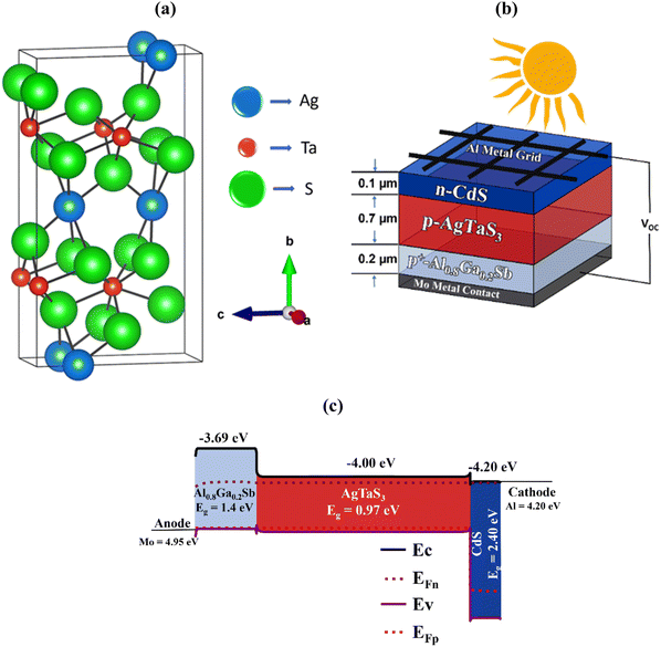 | ||
| Fig. 1 (a) Crystal structure of AgTaS3 perovskite, (b) conceptual diagram, and (c) energy band structure of the AgTaS3-based perovskite SC. | ||
Fig. 1(a) delineates an orthorhombic crystallization of AgTaS3, belonging to the Cmc21 space group featuring lattice constants 3.3755 Å, 14.0608 Å, and 7.7486 Å for a, b, and c, consequently with a unit cell volume, V = 367.77 Å3. The angles alpha, beta, and gamma are each positioned at 90°, indicating an orthogonal phase relationship.19 For the formation of a perovskite structure, charge neutrality must be maintained among the constituent ions. This implies that n(A) + n(B) = 3n(X), where n denotes the valence of the ions A, B, and X.17 This equation ensures that the overall electrical charge within the perovskite structure is balanced, a fundamental criterion for the stability and formation of these materials. Here, n(Ag) + n(Ta) = 1 + 5 = 6 = 3 × 2 = 3n(S) shows the charge neutrality of the AgTaS3 structure.
Fig. 1(b) exhibits the conceptual diagram of the proposed device. CdS is highly stable and is used as the window layer because of its adjustable, wider, direct bandgap, and superior carrier mobility with excellent light transmission properties.20–22 The back surface field (BSF) layer reduces carrier recombination and is composed of Al0.8Ga0.2Sb. Recombination of electrons and holes can reduce the VOC and degrade photo conversion performance.23 AgTaS3 and a highly doped BSF layer create a p–p+ interface and prevent the electrons at the surface from recombining with holes by developing an electric field, thereby increasing the VOC and PCE.24 Previous studies on Si solar cells, with Al0.8Ga0.2Sb BSF layer, have achieved a PCE as high as 38.3%.25 Highly doped p+-Al0.8Ga0.2Sb BSF layer generates an interface with the absorber layer, AgTaS3 as p/p+. AgTaS3 possesses an ionization potential of 4.97 eV with an affinity (EA) of 4 eV. CdS, on the other hand, has an EA of 4.2 eV with an ionization energy of 6.6 eV.
Fig. 1(c) exhibits the illumined band structure of the proposed structure. The BSF layer aligns with the absorber layer as a result of EA, 3.69 eV, and an ionization potential of 5.09 eV of Al0.8Ga0.2Sb. Here, the quasi-Fermi level (QFL) for n-type material, EFn, is just underneath the conduction band, EC, while the QFL for p-type, EFp, is just above the valence band, EV. Sunlight generates electrons at the conduction band of the p–n and p–p+ junction. An aluminium (Al) metal grid acts as a cathode to accumulate electrons. Electrons, moving in the opposite direction, are blocked by the BSF layer and accumulated by Al. Holes are generated in the valence band and acquired by the back contact molybdenum, Mo.
SCAPS-1D employs the Poisson equation, connecting charge to electron and hole continuity equations with the result of the PSC attribute. The Poisson equation, Hole continuity equation, and electron continuity are defined by eqn (1), (2), and (3), respectively:20
 | (1) |
 | (2) |
 | (3) |
 | (4) |
 | (5) |
The effective density of states (DOS) at the conduction band Nc and effective DOS at the valence band Nv can be determined from the following equations:20
 | (6) |
 | (7) |
 and
and  present the electron and hole effective mass for AgTaS3, which have the values of 0.61 and 0.27, which in turn were used to calculate the Nc and Nv of the compound.8
In the simulation, a Gaussian energy distribution is applied to model the defect states in each layer. The defect characterization in the BSF layer is considered neutral, indicating no net charge contribution to the material's conductivity or recombination processes. Conversely, for the window and the absorber layers, defects are modeled as single acceptor types and single donor types, in turn implying that these defects can accept or donate an electron. This distinction in defect modeling is critical for accurately simulating the electronic properties of each layer and their impression on the device's overall efficiency. However, the SCAPS-1D simulator has proved itself to be a reliable one in the era of solar cells that can provides results similar to that obtained from the experimental study as documented in the literature.26–28Table 1 presents the input parameters used for the numerical analysis.
| Parameters | n-CdS20,21 | p-AgTaS38,19 | p+-Al0.8Ga0.2Sb29,30 |
|---|---|---|---|
| Depth (μm) | 0.1 | 0.7 | 0.2 |
| Energy gap (eV) | 2.4 | 0.97 | 1.4 |
| Affinity of electron (eV) | 4.2 | 4.0 | 3.69 |
| Dielectric permittivity | 10 | 13.64 | 12.04 |
| Effective density of states at CB (cm−3) | 2.2 × 10¹⁸ | 1.2 × 10¹⁹ | 7.8 × 10¹⁷ |
| Effective density of states at VB (cm−3) | 1.8 × 10¹⁹ | 3.52 × 10¹⁸ | 1.8 × 10¹⁹ |
| Mobility of electron (cm2 V−1 s−1) | 100 | 12 | 200 |
| Mobility of hole (cm2 V−1 s−1) | 25 | 1.2 | 420 |
| Donor concentration, ND (cm−3) | 1.00 × 10¹⁸ | 0 | 0 |
| Acceptor concentration, NA (cm−3) | 0 | 1.00 × 10¹⁶ | 1.00 × 10¹⁹ |
| Defect concentration (cm−3) | 1.00 × 10¹⁴ | 1.00 × 10¹⁴ | 1.00 × 10¹⁴ |
3. Results and discussion
3.1 Varying the properties of the absorber layer
Fig. 2(a) shows the output characteristics of the proposed device for varying absorbing layer width, concentration of doping and defects for the proposed perovskite-based solar cell. As the width of AgTaS3 ranges from 0.3 μm to 1.1 μm, VOC remains constant at around 0.78 V. However, the insignificant fall in VOC may be the result of a rising dark current with width that increases the possibility of recombination.20 Contrary, the JSC has increased because, in the longer wavelength regime, thicker AgTaS3 absorbs more light and generates a large number of carriers.31 Fill factor (FF) drops sharply from 78.11% to 76.01% because of the shorter carrier lifetime relative to the layer size.32,33 PCE increases from 25.64% to 27.89% up to 0.7 μm of AgTaS3, beyond which recombination of the carriers prevents further increase in PCE.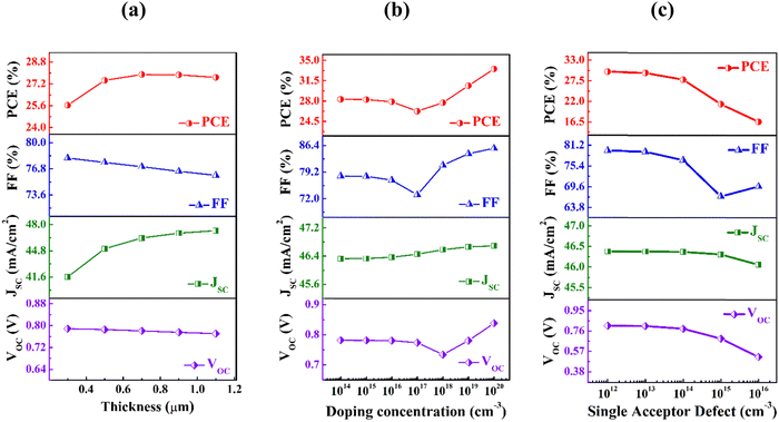 | ||
| Fig. 2 The effects of changing the absorber's (a) breadth, (b) carrier, and (c) defects on the offered cell. | ||
Fig. 2(b) illustrates the impact of carrier densities in AgTaS3 on the perovskite solar cell output characteristics. VOC shows negligible change when the doping varies from 1014 cm−3 to 1018 cm−3. This is because, at lower doping levels, the recombination current decreases, thereby increasing VOC, whereas at higher doping levels, an increment of recombination leads to a reduction in VOC. Then, again, beyond 1018 cm−3, the VOC enhances as recombination decreases. This may happen due to the decrease in the ideality factor, n, with the acceptor concentration.20,34 The fill factor grows proportionally with VOC, and it goes from 78.17% to 85.67%. A modest increase in VOC indicates better FF, as the relation between those is defined by an empirical formula with the help of the diode parameter.20 FF is higher when doping is 1020 cm−3, with the PCE reaching its maximum value at 33.53%.
Fig. 2(c) illustrates the influences of defects on the execution of the PSC. The defect improves the dark current with an increase in Shockley read hall (SRH) recombination and diminishes the performance of the gadget.35 For defects in the range of 1012 cm−3 to 1016 cm−3, VOC changes from 0.81 V to 0.52 V. This significant change affects the FF and PCE and the JSC changes marginally. PCE decreases from 29.91% to 16.62% on account of VOC and FF.
Quantum efficiency (QE) defines the photon absorption efficiency of a perovskite-based SC. No change in QE occurs when acceptor density is varied, as displayed in Fig. 3(a). Enhancing the thickness increases QE proportionally. At 0.7 μm thickness, this structure can absorb around 95% of the incident photons, as seen in the figure. The increment in current density with absorber width is illustrated in Fig. 3(b). The thicker layer can absorb more photons, which increases the photocurrent from 41.6 mA cm−2 current at 0.3 μm to 46.37 mA cm−2 current at 0.7 μm of the thickness. Beyond 0.7 μm, the photocurrent of SC saturates.
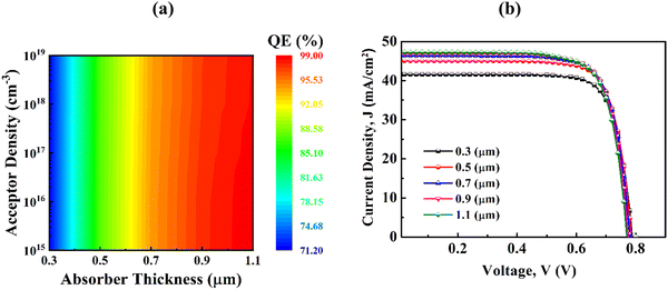 | ||
| Fig. 3 (a) Variation of QE with acceptor density vs. thickness of absorber and (b) current density vs. voltage characteristics with thickness of the absorber. | ||
3.2 Varying the properties of the window layer
Fig. 4 displays the change in output characteristics of the suggested PSC as a result of alteration in the width, carrier concentration and defect volume of the CdS window. Open circuit voltage shows continual behavior at the level of 0.78 V for the thickness of 0.05 μm to 0.25 μm. The FF shows a saturation value of 77%. The JSC drops to 44.65 mA cm−2 from 47.05 mA cm−2 because of an increase in recombination with the breadth of the window.36 The expansion of the breadth in the SC design results in a greater number of photons being absorbed outside the intended space charge region. Absorption mitigates the electron–hole pair generation and intensifies the flow of minority charge carriers, thereby increasing the rate of charge recombination, which negatively impacts the operational efficiency of the solar cell.20 Owing to the increase in recombination, PCE drops to 26.8% at 0.25 μm thickness, whereas it is 28.35% when the thickness is 0.05 μm.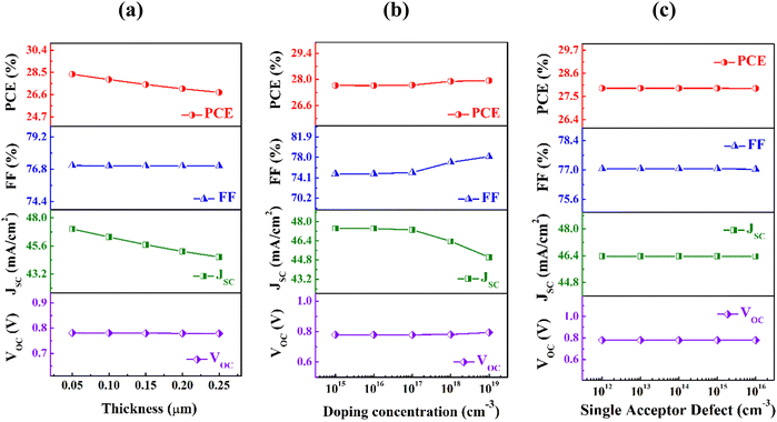 | ||
| Fig. 4 The outcome of change in the window's (a) width, (b) doping volume, and (c) defects on the modeled PSC. | ||
Fig. 4(b) expresses that the photocurrent decreases when the dopant concentration is above 1017 cm−3. The current density remains at 47 mA cm−2 for carriers altering from 1015 to 1017 cm−3. At 1019 cm−3 concentration, it falls to 45 mA cm−2 from 47 mA cm−2. A higher order of doping may lead to parasitic free carrier absorption, which intensifies the recombination level and causes JSC to decrease by 2 mA cm−2.37,38 The VOC does not show any significant change. The fill factor shows a minor change from 74.87% to 78.00% as per the equation below:39
 | (8) |
Fig. 4(c) represents that the defects in the CdS window have no influence on the characteristics of this projected SC. Even as the volume of defects varies within the range of 1012 cm−3 to 1016 cm−3, the shrink in carrier diffusion length as a sequel of diminishing the carrier lifetime is not significant enough with respect to the window breadth.40 Consequently, the performance of the cell is largely consistent.
3.3 Varying the properties of the BSF layer
Fig. 5 demonstrates the consequences of varying the properties of Al0.8Ga0.2Sb BSF on the output characteristics of AgTaS3-based PSC. Fig. 5(a) examines changes in the BSF layer's thickness from 0.1 μm to 0.5 μm, observing its effect on the solar cell's performance. Notably, the VOC remains largely unaffected by this variation, while the JSC shows a marginal increase from 46.36 to 46.38 mA cm−2. This improvement in JSC may be attributed to a stronger electric field at the interface, which effectively reduces the surface recombination velocity. Therefore, the insertion of the BSF layer elevates the cell's efficiency from 20.96% to 27.9%.20,41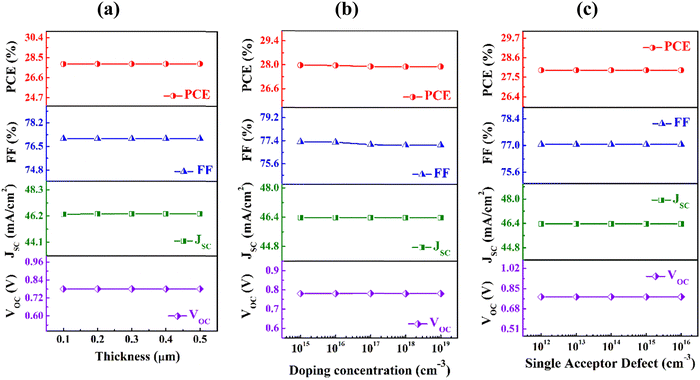 | ||
| Fig. 5 The alteration of cell operation with (a) width, (b) carrier volume and (c) defects of BSF of the n-CdS/p-AgTaS3/p+-Al0.8Ga0.2Sb device. | ||
Fig. 5(b) explores the impact of doping concentrations ranging from 1015 cm−3 to 1018 cm−3. Here, the device current remains almost unchanged. Nonetheless, there is a slight decrease in the FF value to 0.27%, attributed to a lower ratio of generation to recombination.42 This leads to a decrease in the overall PCE from 27.97% to 27.89%.
In Fig. 5(c), the analysis shows that variations in defect density, spanning from 1012 cm−3 to 1016 cm−3, do not significantly affect the performance of the cell. The measurements across this span of bulk defects indicate that they maintain a constant value, suggesting that the defect density in this interval does not substantially influence cell operation. This is a frequent observation in recent studies.20,37,40,42 As carrier diffusion length exceeds the breadth of the BSF layer for these defects, no deterioration is observed in the study.40,42
3.4 Ultimate outcome of AgTaS3 PSC
The exhibition of the contribution of the Al0.8Ga0.2Sb BSF layer is showcased in Fig. 6. The current vs. voltage (J–V) curve is shown in Fig. 6(a). Without the Al0.8Ga0.2Sb layer, the voltage is 0.56 V, photocurrent is 46.22 mA cm−2 and the efficiency is 20.96%. But, with the inclusion of BSF in this PSC structure, the voltage has an incremental value of 0.78 V. The built-in potential created in the p-AgTaS3/p+-Al0.8Ga0.2Sb junction helps to increase the voltage.41 The current of the PSC remains fairly constant. The PCE of the device increased to 27.89%. However, the FF slightly diminishes from 80.87% to 77.06%, which may happen as a consequence of the change in diode properties.20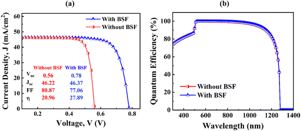 | ||
| Fig. 6 Presentation of (a) J–V, and (b) QE with and without the Al0.8Ga0.2Sb BSF layer of the urged PSC. | ||
Fig. 6(b) reveals the absorption power at different wavelengths of light with and without the BSF layer. From the figure, it is visualized that QE is lower in the wavelength range of 400–500 nm. CdS absorbs a large number of shorter wavelength photons. This absorption results in window gain, which leads to lower QE.43,44 In near 600 nm wavelength, QE increases beyond 95% as the absorber layer absorbs photons of all wavelengths. The BSF layer helps marginally increase quantum efficiency.
Table 2 shows the performance parameters of AgTaS3 PV cells with and without the Al0.8Ga0.2Sb layer. The PCE ascends from 20.96% to 27.89% when the BSF layer is used. The single-junction n-CdS/p-AgTaS3 model has a VOC of 46.22 V and a JSC of 46.22 mA cm−2 with 80.87% FF. The double heterojunction n-CdS/p-AgTaS3/p+-Al0.8Ga0.2Sb has 0.78 V of VOC, 46.37 mA cm−2 of JSC and 77.06% FF. Elevation of the PCE for this double heterojunction solar cell conforms to the detailed balance limit unveiled by Shockley–Queisser (SQ).
| PV parameter | Device structure | |
|---|---|---|
| CdS/AgTaS3 | CdS/AgTaS3/Al0.8Ga0.2Sb | |
| V OC (V) | 0.56 | 0.78 |
| J SC (mA cm−2) | 46.22 | 46.37 |
| FF (%) | 80.87 | 77.06 |
| PCE (%) | 20.96 | 27.89 |
There are many previous reports of various perovskites-based solar cells. Table 3 shows the relative studies on different perovskite solar cells. Organic perovskites have shown impressive performance, but the instability of this type of perovskite makes it a very disadvantageous material. Also, the use of lead halides in SC industries leads to toxicity in the environment. The efficiency and short circuit current density of some previous literature works are much lower than those in this work. Also, the thermal stability of AgTaS3 is superior to that of organic perovskites. These disadvantageous issues make it a preferable material in this era.
| Solar cells | Type | V OC (V) | J SC (mA cm−2) | FF (%) | PCE (%) | Ref. |
|---|---|---|---|---|---|---|
| ZnO/CdS/CH3NH3SnI3/GaAs | Numerical | 0.96 | 33.86 | 73.2 | 23.8 | 21 |
| bl-Y:TiO2/MAPbI3−xClx (solution)/spiro-MeOTAD | Exp. | 1.13 | 22.75 | 75 | 19.3 | 45 |
| FTO/c-TiO2/mTiO2/PbI2:CH3NH3I/spiro-OMeTAD/Au | Exp. | 1.09 | 22.4 | 80 | 19.1 | 46 |
| FTO/SnO2/PCBM/perovskite/spiro-OMeTAD/Ag | Exp. | 1.19 | 19.4 | 79 | 17.9 | 47 |
| mp-TiO2/FAPbI3/MAPbI3 (ETL)/spiro-MeOTAD | Exp. | 1.03 | 20.97 | 74 | 16.01 | 48 |
| ITO/SnO2/MBM/perovskite/spiro-OMeTAD/Ag | Exp. | 1.17 | 24.16 | 81.86 | 24.16 | 49 |
| ITO/AMD PTAA/FA0.9Cs0.1PbI3/PCBM/BCP | Exp. | 1.148 | 24.97 | 83.84 | 23.89 | 50 |
| ITO/P3CT-N/CsPbI3/PCBM/C60/BCP/Ag | Exp. | 1.238 | 20.52 | 80.89 | 20.17 | 51 |
| FTO/c-TiO2/ChPbI3-CsPbI3/Carbon | Exp. | 1.11 | 20.13 | 80.79 | 18.05 | 52 |
| n-CdS/p-AgTaS3/p+-Al0.8Ga0.2Sb | Numerical | 0.78 | 46.37 | 77.06 | 27.89 | This work |
4. Conclusion
AgTaS3-based n-CdS/p-AgTaS3/p+-Al0.8Ga0.2Sb PSC system has been successfully designed and optimized with the help of the SCAPS-1D simulator. Window layer CdS frames a p–n junction with the AgTaS3 absorber layer and this layer produces a p–p+ junction with the Al0.8Ga0.2Sb BSF layer. The depth of the different PSC panels is optimized to 0.7 μm for the absorber layer, 0.1 μm for the window layer, and 0.2 μm for the BSF layer. Doping concentration has been taken as 1.0 × 10¹⁸, 1.0 × 10¹⁶ and 1.0 × 1019 cm−3 for the respective layer. Defect density for Cds, AgTaS3, and Al0.8Ga0.2Sb has been optimized at the value of 1.0 × 1014 cm−3. After optimizing the physical parameters of each layer, the optimal PCE has been up to 27.89%. JSC, VOC, and FF increased to 46.37 mA cm−2, 0.78 V and 77.06%, respectively. VOC has shown an increment from 0.56 V to 0.78 V after adding a thin BSF layer. JSC rises to a small extent after adding the BSF layer from 46.22 mA cm−2 to 46.37 mA cm−2 as a consequence of the reduction in carrier recombination. The p-AgTaS3/p+-Al0.8Ga0.2Sb junction produces a high potential barrier and raises the VOC as well as the PCE. This result paves the way for a highly efficient AgTaS3 inorganic perovskite solar cell.Author contributions
Tanvir Ahmed: data curation; formal analysis; investigation; validation; writing – original draft (equal). Md. Choyon Islam: formal analysis; validation; writing – original draft. Md. Alamin Hossain Pappu: data curation; formal analysis; validation; writing – original draft. Md. Islahur Rahman Ebon: formal analysis; investigation; validation; writing – original draft. Sheikh Noman Shiddique: formal analysis; investigation; validation; writing – original draft. Mainul Hossain: formal analysis; investigation; validation; writing – original draft. Jaker Hossain: conceptualization; formal analysis; methodology; supervision; validation; writing – original draft; writing – review and editing.Data availability
Data will be available from the corresponding author upon reasonable request.Conflicts of interest
There are no conflicts to declare.Acknowledgements
The authors highly appreciate Dr Marc Burgelman, University of Gent, Belgium, for providing SCAPS simulation software.References
- Y. Liu, Y. Li, Y. Wu, G. Yang, L. Mazzarella, P. Procel-Moya, A. C. Tamboli, K. Weber, M. Boccard, O. Isabella, X. Yang and B. Sun, High-Efficiency Silicon Heterojunction Solar Cells: Materials, Devices and Applications, Mater. Sci. Eng., R, 2020, 142, 100579, DOI:10.1016/j.mser.2020.100579.
- E. Płaczek-Popko, Top PV market solar cells 2016, Opto-Electron. Rev., 2017, 25(2), 55–64, DOI:10.1016/j.opelre.2017.03.002.
- G. S. Alzahrani, F. S. Alzahrani and A. M. Nahhas, Study of the Specific Factors Effecting the PV Solar Cell’s Efficiency in Saudi Arabi, Sustainable Energy, 2020, 8(1), 6–11 Search PubMed.
- J. Jeong, M. Kim, J. Seo, H. Lu, P. Ahlawat, A. Mishra and J. Y. Kim, Pseudo-halide anion engineering for α-FAPbI3 perovskite solar cells, Nature, 2021, 592(7854), 381–385, DOI:10.1038/s41586-021-03406-5.
- A. B. Djurišić, F. Z. Liu, H. W. Tam, M. K. Wong, A. Ng, C. Surya, W. Chen and Z. B. He, Perovskite solar cells - An overview of critical issues, Prog. Quantum Electron., 2017, 53, 1–37, DOI:10.1016/j.pquantelec.2017.05.
- A. Babayigit, A. Ethirajan, M. Muller and B. Conings, Toxicity of organometal halide perovskite solar cells, Nat. Mater., 2016, 15(3), 247–251, DOI:10.1038/nmat4572.
- J. Duan, H. Xu, W. E. I. Sha, Y. Zhao, Y. Wang, X. Yang and Q. Tang, Inorganic perovskite solar cells: An emerging member in photovoltaic community, J. Mater. Chem. A, 2019, 7, 21036–21068, 10.1039/C9TA06674H.
- K. Kuhar, A. Crovetto, M. Pandey, K. S. Thygesen, B. Seger, P. C. Vesborg, O. Hansen, I. Chorkendorff and K. W. Jacobsen, Sulfide perovskites for solar energy conversion applications: computational screening and synthesis of the selected compound LaYS3, Energy Environ. Sci., 2017, 10(12), 2579–2593, 10.1039/C7EE02702H.
- D. Ju, X. Jiang, H. Xiao, X. Chen, X. Hu and X. Tao, Narrow band gap and high mobility of lead-free perovskite single crystals Sn-doped MA3Sb2I9, J. Mater. Chem., 2018, 6, 20753–20759, 10.1039/c8ta08315k.
- J. Heo, L. Yu, E. Altschul, B. E. Waters, J. F. Wager, A. Zunger and D. A. Keszler, CuTaS3: Intermetal d–d Transitions Enable High Solar Absorption, Chem. Mater., 2017, 29(6), 2594–2598, DOI:10.1021/acs.chemmater.6b04730.
- M. A. Green, A. Ho-Baillie and H. Snaith, The emergence of perovskite solar cells, Nat. Photon., 2014, 8, 506–514, DOI:10.1038/nphoton.2014.134.
- C. Liu, Z. He, Y. Li, A. Liu, R. Cai, L. Gao and T. Ma, Sulfur contributes to stable and efficient carbon-based perovskite solar cells, J. Colloid Interface Sci., 2022, 605, 54–59, DOI:10.1016/j.jcis.2021.07.058.
- Y. Zhou, C. Liu, F. Meng, C. Zhang, G. Wei, L. Gao and T. Ma, Recent progress in perovskite solar cells modified by sulfur compounds, Sol. RRL, 2021, 5(4), 2000713 CrossRef CAS.
- Z. Ma, Y. Wang, Y. Lu, H. Ning and J. Zhang, Tackling Challenges in Perovskite-Type Metal Oxide Photocatalysts, Energy Technol., 2021, 9(5), 2001019, DOI:10.1002/ente.202001019.
- W.-G. Li, H.-S. Rao, B.-X. Chen, X.-D. Wang and D.-B. Kuang, A form a midinium–methylammonium lead iodide perovskite single crystal exhibiting exceptional optoelectronic properties and long-term stability, J. Mater. Chem. A, 2017, 5(36), 19431–19438, 10.1039/c7ta04608a.
- B. Yang, O. Dyck, J. Poplawsky, J. Keum, A. Puretzky, S. Das and K. Xiao, Perovskite Solar Cells with Near 100% Internal Quantum Efficiency Based on Large Single Crystalline Grains and Vertical Bulk Heterojunctions, J. Am. Chem. Soc., 2015, 137(29), 9210–9213, DOI:10.1021/jacs.5b03144.
- S. J. Adjogri and E. L. Meyer, Chalcogenide Perovskites and Perovskite-Based Chalcohalide as Photoabsorbers: A Study of Their Properties, and Potential Photovoltaic Applications, Materials, 2021, 14(24), 7857, DOI:10.3390/ma14247857.
- Y. Chen, L. Zhang, Y. Zhang, H. Gao and H. Yan, Large-area perovskite solar cells – a review of recent progress and issues, RSC Adv., 2018, 8(19), 10489–10508, 10.1039/c8ra00384j.
- H. Wada, M. Onoda and H. Nozaki, Structure and properties of a new compound AgTaS3, J. Solid State Chem., 1992, 97(1), 29–35, DOI:10.1016/0022-4596(92)90005-g.
- M. A. H. Pappu, A. Kuddus, B. K. Mondal, A. T. Abir and J. Hossain, Design of n-CdS/p-CuInTe2/p + -MoS2 thin film solar cell with a power conversion efficiency of 34.32%, Opt. Continuum, 2023, 2(4), 942–955, DOI:10.1364/OPTCON.486044.
- S. Tripathi, L. P. Sadanand and D. K. Dwivedi, Contribution to sustainable and environmental friendly non-toxic CZTS solar cell with an innovative hybrid buffer layer, Sol. Energy, 2020, 204, 748–760 CrossRef CAS.
- I. Qasim, O. Ahmad, A. Rashid, T. Zehra, M. I. Malik, M. Rashid, W. Ahmed and F. Nasir, Numerical optimization of (FTO/ZnO/CdS/CH3NH3SnI3/GaAs/Au) perovskite solar cell using solar capacitance simulator with efficiency above 23% predicted, Opt. Quant. Electron., 2021, 53, 713, DOI:10.1007/s11082-021-03361-5.
- M. A. Islam, Y. Sulaiman and N. Amin, A Comparative study of BSF layers for ultra-thin CdS:O/CdTe solar cells, Chalcogenide Lett., 2011, 8(2), 65–75 CAS.
- J. G. Fossum, Physical Operation of Back-Surface-Field Silicon Solar Cells, IEEE Trans. Electron Devices, 1977, 24(4), 322–325, DOI:10.1109/T-ED.1977.18735.
- M. A. Green, Intrinsic concentration, effective densities of states, and effective mass in silicon, J. Appl. Phys., 1990, 67(6), 2944–2954, DOI:10.1063/1.345414.
- L. Huang, X. Sun, C. Li, R. Xu, J. Xu, Y. Du, Y. Wu, J. Ni, H. Cai, J. Li, Z. Hu and J. Zhang, Electron transport layer-free planar perovskite solar cells: Further performance enhancement perspective from device simulation, Sol. Energy Mater. Sol. Cells, 2016, 157, 1038–1047 CrossRef CAS.
- K. Decock, P. Zabierowski and M. Burgelman, Modeling metastabilities in chalcopyrite-based thin film solar cells, J. Appl. Phys., 2012, 111(4), 043703 CrossRef.
- S. Valsalakumar, S. Bhandari, T. K. Mallick, J. Hinshelwood and S. Sundaram, Experimental Validation of Optimized Solar Cell Capacitance Simulation for Rheology-Modulated Carbon-Based Hole Transport Layer-Free Perovskite Solar Cell, Adv. Energy Sustainability Res., 2024, 2300244 CrossRef.
- J. Hossain, Design and simulation of double-heterojunction solar cells based on Si and GaAs wafers, J. Phys. Commun., 2021, 5(8), 085008, DOI:10.1088/2399-6528/ac1bc0.
- R. Dhakal, Y. Huh, D. Galipeau and X. Yan, AlSb Compound Semiconductor as Absorber Layer in Thin Film Solar Cells, Solar Cells - New Aspects and Solutions, InTech, 1st edn, 2011, pp. 341–356 DOI:10.5772/21375.
- Q. Lin, A. Armin and R. Nagiri, et al., Electro-optics of perovskite solar cells, Nat. Photon., 2015, 9, 106–112, DOI:10.1038/nphoton.2014.284.
- T. M. Koh, T. Krishnamoorthy, N. Yantara, C. Shi, W. L. Leong, P. P. Boix, A. C. Grimsdale, S. G. Mhaisalkar and N. Mathews, Formamidinium tin-based perovskite with low Eg for photovoltaic applications, J. Mater. Chem. A, 2015, 3(29), 14996–15000, 10.1039/C5TA00190K.
- A. Taraa, V. Bhartib, S. Sharmaa and R. Gupta, Device simulation of FASnI3 based perovskite solar cell with Zn(O0.3, S0.7) as electron transport layer using SCAPS-1D, Opt. Mater., 2021, 119, 111362, DOI:10.1016/j.optmat.2021.111362.
- M. A. H. Pappu, S. N. Shiddique, B. K. Mondal, M. I. R. Ebon, T. Ahmed and J. Hossain, Numerical simulation on an efficient n-CdS/p-ZnSnN2/p + -Cu2SnS3/p+ +- CuGaSe2 thin film solar cell, Mater. Today Commun., 2024, 38, 108474 CrossRef CAS.
- J. Hossain, B. K. Mondal and S. K. Mostaque, Design of a highly efficient FeS2-based dual-heterojunction thin film solar cell, Int. J. Green Energy, 2022, 19(14), 1531–1542, DOI:10.1080/15435075.2021.2011291.
- K. Mukhopadhyay, H. I. P. Fermi and J. P. Joseph, Thickness optimization of CdS/ZnO hybrid buffer layer in CZTSe thin film solar cells using SCAPS simulation program, Mater. Res. Innovations, 2019, 23(6), 319–329, DOI:10.1080/14328917.2018.1475907.
- B. Saha, B. K. Mondal, S. K. Mostaque, M. Hossain and J. Hossain, Numerical modeling of CuSbSe2-based dual-heterojunction thin film solar cell with CGS back surface layer, AIP Adv., 2023, 13(2), 025255, DOI:10.1063/5.0133889.
- D. A. Clugston and P. A. Basore, Modelling free-carrier absorption in solar cells, Prog. Photovoltaics Res. Appl., 1997, 5, 229–236 CrossRef CAS.
- P. Sidi; D. Sukoco; W. Purnomo; H. Sudibyo and D. Hartanto In Electric Energy Management and Engineering in Solar Cell System, Solar Cells - Research and Application Perspectives, InTech, 1st edn, 2013, pp. 327–351 DOI:10.5772/52572.
- M. S. Hossen, A. T. Abir and J. Hossain, Design of an efficient AgInSe2 chalcopyrite-based heterojunction thin film solar cell, Energy Technol., 2023, 11(8), 2300223 CrossRef CAS.
- J. G. Fossum, Physical Operation of Back-Surface-Field Silicon Solar Cells, IEEE Trans. Electron Devices, 1977, 24(4), 322–325, DOI:10.1109/T-ED.1977.18735.
- N. J. Konok, S. K. Mostaque and J. Hossain, Design of a High Efficiency p-Si Based Heterojunction Solar Cell with ln2S3 Window and NiO BSF Layers, Silicon, 2024, 1–10, DOI:10.1007/s12633-024-02940-x.
- G. A. Nowsherwan, M. A. Iqbal and S. U. Rehman, et al., Numerical optimization and performance evaluation of ZnPC: PC70BM based dye-sensitized solar cell, Sci. Rep., 2023, 13, 10431, DOI:10.1038/s41598-023-37486-2.
- S. R. Kodigala, Chapter 8 – Cu(In1−xGax)Se2 and CuIn(Se1−xSx)2 Thin Film Solar Cells, Thin Films Nanostruct., 2010, 35, 505–679, DOI:10.1016/b978-0-12-373697-0.00008-0.
- H. Zhou, Q. Chen, G. Li, S. Luo, T.-B. Song, H.-S. Duan, Z. Hong, J. You, Y. Liu and Y. Yang, Interface engineering of highly efficient perovskite solar cells, Science, 2014, 345(6196), 542–546, DOI:10.1126/science.1254050.
- C. Roldán-Carmona, P. Gratia, I. Zimmermann, G. Grancini, P. Gao, M. Graetzel and M. K. Nazeeruddin, High efficiency methylammonium lead triiodide perovskite solar cells: the relevance of non-stoichiometric precursors, Energy Environ. Sci., 2015, 8(12), 3550–3556, 10.1039/c5ee02555a.
- D. P. McMeekin, G. Sadoughi, W. Rehman, G. E. Eperon, M. Saliba, M. T. Horantner, A. Haghighirad, N. Sakai, L. Korte, B. Rech, M. B. Johnston, L. M. Herz and H. J. Snaith, A mixed-cation lead mixed-halide perovskite absorber for tandem solar cells, Science, 2016, 351(6269), 151–155, DOI:10.1126/science.aad5845.
- J.-W. Lee, D.-J. Seol, A.-N. Cho and N.-G. Park, High-Efficiency Perovskite Solar Cells Based on the Black Polymorph of HC(NH2)2PbI3, Adv. Mater., 2014, 26(29), 4991–4998, DOI:10.1002/adma.201401137.
- Y. Sun, J. Zhang, B. Yu, S. Shi and H. Yu, Regulate defects and energy levels for perovskite solar cells by co-modification strategy, Nano Energy, 2024, 121, 109245 CrossRef CAS.
- J. Zhang, B. Yu, Y. Sun and H. Yu, Minimized Energy Loss at the Buried Interface of p-i-n Perovskite Solar Cells via Accelerating Charge Transfer and Forming p–n Homojunction, Adv. Energy Mater., 2023, 13, 2300382, DOI:10.1002/aenm.202300382.
- N. Sun, S. Fu, Y. Li, L. Chen, J. Chung, M. M. Saeed, K. Dolia, A. Rahimi, C. Li, Z. Song and Y. Yan, Tailoring Crystallization Dynamics of CsPbI3 for Scalable Production of Efficient Inorganic Perovskite Solar Cells, Adv. Funct. Mater., 2024, 34, 2309894, DOI:10.1002/adfm.202309894.
- J. Zhang, G. Zhang, P.-Y. Su, R. Huang, J. Lin, W. Wang, Z. Pan, H. Rao and X. Zhong, 1D Choline-PbI3-Based Heterostructure Boosts Efficiency and Stability of CsPbI3 Perovskite Solar Cells, Angew. Chem., Int. Ed., 2023, 62(25), e202303486 CrossRef CAS PubMed.
| This journal is © The Royal Society of Chemistry 2024 |
