
 Open Access Article
 This Open Access Article is licensed under a Creative Commons Attribution-Non Commercial 3.0 Unported Licence
Enhancing perovskite solar cell efficiency and stability through the incorporation of BDAI2 and DMPDAI2†
Han Wen
Chang‡
,
Chien Cheng
Li‡
,
Tzu Yu
Haung
,
Hsin Chieh
Li
and
Chih Shan
Tan
 *
*
Institute of Electronics, National Yang Ming Chiao Tung University, Hsinchu 30010, Taiwan. E-mail: cstan@nycu.edu.tw
First published on 26th January 2024
Abstract
This research explores the incorporation of 2D materials, BDAI2 and DMPDAI2, into perovskite solar cells, demonstrating enhanced efficiency and stability in the resulting devices. These materials facilitate the formation of quasi-2D perovskite layers, leading to denser films and smaller grain sizes. Through extensive analyses, including XRD, XPS, and UPS, this study highlights the structural and electronic modifications induced by these 2D materials, resulting in improved conductivity and carrier mobility. Additionally, Sentaurus TCAD simulations validate the observed increase in power conversion efficiency (PCE), supporting the experimental findings. Integrating BDAI2 and DMPDAI2 presents a promising approach for optimizing perovskite solar cells’ performance and reliability.
Introduction
Perovskite solar cells (PSCs) have garnered substantial attention from academia and industry as promising emerging technologies in the solar cell domain. Miyasaki and colleagues initiated a perovskite device's initial proposition and fabrication in 2006, with a conversion efficiency recorded at 3.81%.1 Subsequently, the introduction of Spiro-OMeTAD—a solid-state material—by Kim, Park, Grätzel, and others in 2012 as the hole transport layer yielded enhanced stability and a significant efficiency increase to 9.7%.2 Shortly after that, Snaith and associates utilized Spiro-OMeTAD to develop a novel perovskite material, CH3NH3PbI2Cl, demonstrating elevated stability, carrier mobility, and photovoltaic conversion efficiency of 10.9%.3In a pivotal moment in July 2013, Grätzel's team improved the morphology of mesoporous TiO2 films through a two-step deposition method, achieving a certified efficiency of 14.1%.4 This breakthrough marked the inception of remarkable advancements in the efficiency of PSCs, drawing many researchers into the field. Over the span from 2009 to 2023, efficiency levels have risen from 3.9% to an impressive 26%. Despite the inverted perovskite solar cell (p–i–n) showcasing lower photovoltaic conversion efficiency compared to its counterpart, the normal perovskite solar cell (n–i–p),5–7 it has nevertheless garnered widespread attention owing to its advantageous low-temperature processing and enhanced durability.
One of the formidable challenges facing PSCs is the chemical instability inherent to their organic–inorganic crystal structure. To mitigate this, one viable strategy is the incorporation of two-dimensional (2D) perovskites infused with long-chain hydrophobic organic cations. These large organic cations confer hydrophobic characteristics to 2D perovskites as a barrier to moisture penetration and subsequent degradation of the perovskite. Notably, the formation process of 2D perovskites is less restricted by tolerance factors compared to their three-dimensional (3D) counterparts,8,9 with the latter constrained to a tolerance factor ranging between 0.8 and 1.10 This inherent characteristic affords greater latitude in the selection of materials, thereby offering flexibility in developing and optimizing PSCs.
Despite their hydrophobic properties, 2D perovskites present several disadvantages, including undesired crystal orientation, comparatively low mobility,11 and specific face accumulation. These materials form layered structures that hinder carrier migration and reduce the passivation effect.12 Additionally, the 2D materials used in our study, classified as RP perovskites, possess van der Waals gaps that may induce layer sliding, resulting in phase instability.13
To amalgamate the advantages while mitigating the disadvantages of both perovskite types, researchers have introduced the concept of 2D/3D hybrid perovskites. This innovative approach leverages the 2D structure to improve perovskites’ grain and film characteristics, thereby enhancing efficiency and stability.14
In the present study, our initial experiments involved testing six different two-ammonium-based 2D materials, each with two NH3+ ends: BDAI2, DMPDAI2, BZDAI2, ADI2, DABCODI2, and EDAI2. Following rigorous testing, we selected BDAI2 and DMPDAI2 (t1) to develop a 2D/3D hybrid structure. The introduction of hydrogen bonding between organic cations and BX64− anions leads to structural modifications in the octahedral configuration, resulting in a stable 2D perovskite structure with reduced sliding.
In 2023, Chih Shan Tan computed the phonon density of states (DOS) for structures based on two-ammonium aromatic spacer cations and found a reduced imaginary component in the phonon DOS. This reduction typically indicates enhanced dynamic stability, aligning with our experimental findings of increased stability.10,15 Such structural improvements notably enhance the crystal structure's resilience against heat and water molecules. Furthermore, the symmetric 2D materials employed in our study effectively minimize the oxidation of Pb ions within the perovskite while simultaneously regulating the crystallization process.16,17
Method
Materials
The hole transport material utilized was poly(3,4-ethylenedioxythiophene)–poly(styrenesulfonate) (PEDOT:PSS), procured from Heraeus® Clevios TMP VP AI 4083. The perovskite layer was fabricated using various compounds: cesium iodide (CsI, 99.999%), and methylammonium bromide (MABr, 98%) were obtained from Sigma-Aldrich; formamidinium iodide (FAI) was sourced from Great Cell; lead(II) bromide (PbBr2, 99.99999%) was acquired from echochemical; and lead iodide (PbI2, 99.999%) was provided by Alfa Aesar. [6,6]-Phenyl C61 butyric acid methyl ester (PCBM, 99%) was procured from Sigma-Aldrich as the electron transport material. Furthermore, the interfacial layer material, 2,9-dimethyl-4,7-diphenyl-1,10-phenanthroline (BCP), was obtained from Lumtec.For the fabrication of diammonium-based perovskite films, several distinct compounds were employed. These compounds comprised butane-1,4-diammonium iodide (BDAI2), 2,2-dimethylpropane-1,3-diammonium iodide (DMPDAI2), 1,4-benzenediammonium iodide (BZDAI2), acetamidinium iodide (ADI2), 1,4-diazabicyclo[2,2,2]octane-1,4-diium iodide (DABCODI2), and ethane-1,2-diammonium iodide (EDAI2). Each of these was obtained from Great Cell.
Device fabrication
The ITO glass substrates underwent a sequential ultrasonication process in acetone and alcohol, each for 30 minutes. The substrates were dried using a nitrogen gun and treated with UV ozone for another 30 minutes. The PEDOT solution, the hole-transporting layer, was spin-coated onto these prepared substrates at 4500 rpm for 45 seconds, followed by annealing at 120 °C for 10 minutes.The perovskite precursor solution was formulated with a composition of (Cs0.05MA0.16FA0.79)Pb(I0.84Br0.16)3. This was achieved by dissolving predetermined quantities of CsI, MABr, FAI, PbBr2, and PbI2 in a solvent mixture of DMF and DMSO (volume ratio of 4![[thin space (1/6-em)]](https://www.rsc.org/images/entities/char_2009.gif) :1). Compounds BDAI2, DMPDAI2, BZDAI2, ADI2, DABCODI2, and EDAI2 were introduced into the solution at adjusted concentrations of 1% molar concentration each. The spin-coating process of the perovskite layer was carried out at 500 rpm for 7 seconds and then at 4500 rpm for 33 seconds. This process incorporated a swift wash with 500 μL of chlorobenzene as an antisolvent. The coated substrates were annealed on a hotplate set at 100 °C for 20 minutes.
:1). Compounds BDAI2, DMPDAI2, BZDAI2, ADI2, DABCODI2, and EDAI2 were introduced into the solution at adjusted concentrations of 1% molar concentration each. The spin-coating process of the perovskite layer was carried out at 500 rpm for 7 seconds and then at 4500 rpm for 33 seconds. This process incorporated a swift wash with 500 μL of chlorobenzene as an antisolvent. The coated substrates were annealed on a hotplate set at 100 °C for 20 minutes.
After this, the electron transport layer composed of PCBM (20 mg mL−1 in chlorobenzene) was spin-coated atop the perovskite layer, with the process set at 2500 rpm for 30 seconds. To further optimize the device structure, a saturated solution of BCP in methanol was spin-coated onto the PCBM layer at a speed of 4000 rpm for 30 seconds, acting as the interfacial layer. The device was finalized with the thermal evaporation of a 100 nm-thick layer of silver (Ag) in a vacuum chamber.
Results and discussion
Fig. 1 shows the molecular structures of BDA and DMPDA. Fig. 2a delineates the structure of the inverted perovskite solar cells employed in this study, while Fig. 2b displays the six selected symmetrical ammonium-based 2D materials. Notably, BDAI2 and DMPDAI2 outperformed the others in terms of efficiency compared to devices devoid of 2D materials, thereby becoming the focal point of subsequent analyses and the devices integrating them.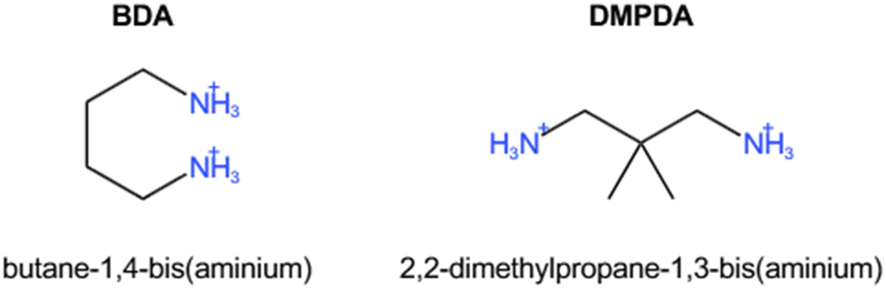 | ||
| Fig. 1 The molecular architectures of BDA and DMPDA. | ||
 | ||
| Fig. 2 The structure, performance, and AFM analysis of symmetric diammonium-based quasi-2D perovskite solar cells are depicted. (a) An illustration of the structural layout of inverted planar perovskite solar cells (PSCs) is presented. (b) PCE statistics for ten devices, each for the added perovskite and quasi-2D solar cells, are provided. (c) With or without symmetric diammonium ligand treatment, J–V curves for the champion devices are displayed in the forward scan direction. (d) Long-term stability tests for PSCs—untreated, treated with BDAI2, and treated with DMPDAI2—are conducted in dark ambient conditions at 60% relative humidity and 20 °C without encapsulation. AFM images for (e) untreated perovskite, (f) BDAI2-treated, and (g) DMPDAI2-treated perovskite films are also provided. | ||
The elemental composition within each layer and the overall device structure—incorporating the ammonium-based materials—were ascertained through Secondary Ion Mass Spectrometer (SIMS) analysis. Fig. S1 (found in the ESI,† with comprehensive data in Table S1) divulges the results, highlighting that introducing 2D materials exerts a negligible influence on the elemental distribution across the device layers. Fig. 2c illustrates the current density–voltage (J–V) curves of the three variations of perovskite devices, with the corresponding detailed data tabulated in Table 1. Including BDAI2 and DMPDAI2 is implicated in the noteworthy enhancement of the power conversion efficiency (PCE). As substantiated by the literature,18 long carbon chains appended with ammonium groups are renowned for their exemplary passivation effects. This phenomenon is corroborated by our data, showing that BDAI2 and DMPDAI2 proficiently passivate surface defects in the perovskite, facilitating improved charge extraction and surpassing the performance of perovskites without 2D materials.19
| J sc (mA cm−2) | V oc (V) | FF (%) | PCE (%) | |
|---|---|---|---|---|
| Without | 16.55 | 0.921 | 83.40 | 12.71 (10.12) |
| BDAI2 | 26.92 | 0.988 | 78.87 | 20.99 (12.68) |
| DMPDAI2 | 22.45 | 0.868 | 83.84 | 16.33 (11.26) |
Fig. 2d documents the results of the stability test. Following a week in dark ambient conditions—characterized by 60% relative humidity and a temperature of 20 °C without encapsulation—the device embedded with BDAI2 maintained 90% of its initial efficiency. The devices incorporating DMPDAI2 exhibited slightly diminished retention at 75%, whereas the reference device retained a mere 44%. These findings underscore the stability-enhancing effects of adding 2D materials to the devices.
Moreover, atomic force microscopy (AFM) analysis was executed to examine the surface topology of the perovskite films. Fig. 2e–g visually represent this analysis, revealing that films with integrated 2D materials substantially reduce surface roughness (RMS) relative to their untreated counterparts. This diminution in roughness can be attributed to smaller grain sizes and denser films, culminating in smoother surface topographies.
Fig. 3a presents the X-ray diffraction (XRD) patterns for the three devices under consideration. To elucidate the impact of incorporating BDAI2 and DMPDAI2 into the perovskite structure, we started by comparing their respective XRD peaks. The XRD patterns of the perovskites containing these materials retain the characteristic peaks of 3D perovskites, with the principal (100) peak identified at 14°. An auxiliary peak, denoted by a triangle symbol (▲) above at 12°, signals the presence of surplus PbI2 in the 3D perovskite film. However, the integration of 2D materials yielded no substantial peaks at 12°, suggesting the complete conversion of PbI2 into the perovskite material. Moreover, we can observe a small peak at 8°, marked with an asterisk (*) above. This signifies a subtle 2D signal, but since we have added only a small amount, the signal is not significant. This result is consistent with previous research findings.20,21 Further analysis of the (100) signal, considering the full width at half maximum (FWHM) and grain size (detailed in Table S2, ESI†), reveals that the incorporation of BDAI2 and DMPDAI2 leads to denser films and smaller grain sizes—findings consistent with those obtained through atomic force microscopy (AFM).
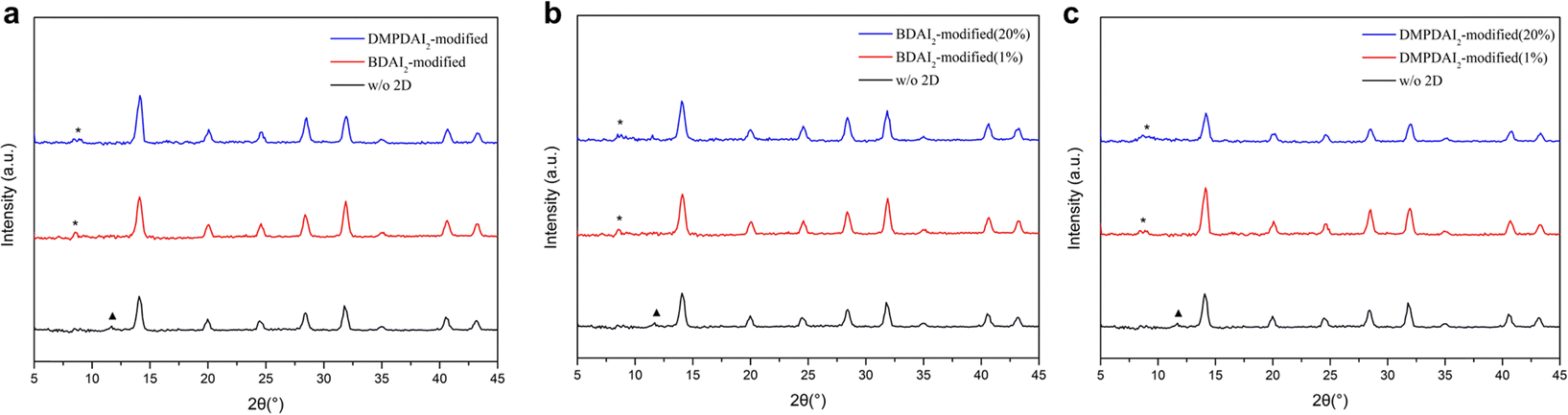 | ||
| Fig. 3 XRD patterns of symmetric diammonium-based quasi-2D perovskites are presented. (a) Displays the X-ray diffraction (XRD) patterns of perovskite films without 2D treatment, those treated with BDAI2, and those treated with DMPDAI2. Furthermore, XRD patterns with varying amounts of (b) BDAI2 and (c) DMPDAI2 are depicted. | ||
In addition, escalating concentrations of BDAI2 and DMPDAI2 did not have a significant impact on the XRD results (as seen in Fig. 3b and c). Comparing the XRD patterns of perovskites with the addition of 1% BDAI2 and 20% BDAI2, we observe that the two patterns are nearly identical. We speculate that the low solubility of BDAI2 in DMF/DMSO might be the reason. It's possible that 1% of BDAI2 reached saturation, and any undissolved components were filtered out. Similarly, the situation is the same for DMPDAI2 as well.
X-ray photoelectron spectroscopy (XPS) was employed to substantiate the formation of quasi-2D perovskite layers further. Correcting for external carbon contamination, the XPS data are presented in Fig. 4a–c. The conspicuous peaks in the data correspond to the carbon–carbon bond (C–C) at 284.8 eV, the C–NH2 bond from MA at 286 eV, and the N–C![[double bond, length as m-dash]](https://www.rsc.org/images/entities/char_e001.gif) N bond from FA. The areas under these peaks were quantified and are available in Table S3 (ESI†). Due to the elongated carbon chain (C4) inherent to BDAI2, the peak corresponding to C–C bonds is predominant, showcasing the largest integrated area. However, this phenomenon was absent for DMPDAI2, attributed to its distinct molecular structure. Furthermore, owing to the emergence of the quasi-2D perovskite structure, there was a significant diminution in the CH3NH3+ peak relative to the 3D perovskite.
N bond from FA. The areas under these peaks were quantified and are available in Table S3 (ESI†). Due to the elongated carbon chain (C4) inherent to BDAI2, the peak corresponding to C–C bonds is predominant, showcasing the largest integrated area. However, this phenomenon was absent for DMPDAI2, attributed to its distinct molecular structure. Furthermore, owing to the emergence of the quasi-2D perovskite structure, there was a significant diminution in the CH3NH3+ peak relative to the 3D perovskite.
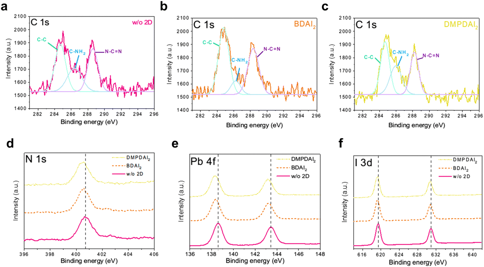 | ||
| Fig. 4 The high-resolution X-ray photoelectron spectroscopy (XPS) analyses of C 1s elements for (a) perovskite films without 2D treatment, (b) BDAI2-treated perovskite films, and (c) DMPDAI2-treated perovskite films. Additionally, it includes XPS spectra for (d) N 1s, (e) Pb 4f, and (f) I 3d elements across the three types of films: those untreated, those treated with BDAI2, and those treated with DMPDAI2. | ||
The inclusion of diammonium in the perovskite influences the hydrogen bonding dynamics among FA and I, Pb–I bonding, and the hydrogen bonds between PbI and adjacent I atoms.22–24 The stretching imposed by diammonium cations reduces the bonding strength of FA–I, leading to a consequent decline in bond energy,13 as illustrated in Fig. 4d. These intensified interactions culminate in the Pb–I bond length elongating, correlating to weakened bond strength. Fig. 4e and f show that introducing 2D materials into perovskites influences the Pb–I bond strength due to structural modifications, evidenced by an overall shift of the peak towards lower binding energies.
The presence of diammonium within the perovskite structure is unequivocally confirmed through the analysis of C 1s, N 1s, Pb 4f, and I 3d spectra. The quasi-2D perovskite structure inherently masks some molecular information25—the three-dimensional arrangement of diammonium within the perovskite results in decreased bond energies. Collectively, the data corroborate the formation of quasi-2D perovskite layers.
Tauc plots and ultraviolet photoelectron spectroscopy (UPS) measurements were utilized to ascertain the widths of the bandgaps and the energy of the valence bands for each layer, as depicted in Fig. S2 and S3 (ESI†). The results denote that while introducing 2D materials does not notably influence the bandgap, it does induce a slight shift in the valence band energy. The band positions of the various perovskite devices are detailed in Table S4 (ESI†).
Electrical data, including enhancements in conductivity and carrier mobility, were garnered through Hall measurements, which are compiled in Table 2. These improvements are mirrored in the augmentation of the power conversion efficiency (PCE), underscoring the pivotal role of quasi-2D perovskite structures in optimizing perovskite devices.
| Conductivity (S cm−1) | Mobility (cm2 V−1 s−1) | Carrier concentration (cm−3) | |
|---|---|---|---|
| Without | 2.35 × 10⁻² | 5.1 | 2.88 × 10¹⁶ |
| BDAI2 | 5.87 × 10⁻² | 18.0 | 2.04 × 10¹⁶ |
| DMPDAI2 | 4.89 × 10⁻² | 13.6 | 2.25 × 10¹⁶ |
Sentaurus TCAD simulations were conducted to validate our experimental findings, with the pertinent parameters for these simulations enumerated in Table S5 (ESI†).26–28Fig. 5 and Table 3 encapsulate the simulation outcomes. Specifically, Fig. 5 illustrates the current density–voltage (J–V) curve for simulated devices, and Table 3 catalogs the photovoltaic parameters derived from these simulations. A comparative analysis between Table 1 and Table 3 reveals that although the simulated PCE slightly eclipses the average experimental PCE, the observed trends align consistently across both data sets. The pinnacle of PCE is attained by incorporating BDAI2, succeeded closely by DMPDAI2, with the 3D perovskite trailing behind.
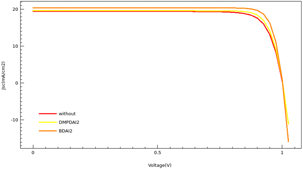 | ||
| Fig. 5 The J–V curves generated through TCAD simulations are presented for perovskite solar cells (PSCs) without 2D treatment, those treated with BDAI2, and those treated with DMPDAI2. | ||
| J sc (mA cm−2) | V oc (V) | FF (%) | PCE (%) | |
|---|---|---|---|---|
| Without | 19.42 | 1.001 | 82.83 | 16.11 |
| BDAI2 | 20.40 | 1.001 | 86.81 | 17.73 |
| DMPDAI2 | 19.60 | 1.002 | 85.07 | 16.71 |
It is crucial to note that Sentaurus TCAD simulations operate under ideal conditions. Conversely, experimental procedures are susceptible to many external factors that could precipitate a decline in PCE. Consequently, a discernible discrepancy persists between theoretical projections and empirical outcomes. For those devices whose efficiencies ostensibly surpass the simulated values, we conjecture that this disparity emanates from measurement inaccuracies, particularly those regarding errors in gauging light intensity.
Conclusion
This comprehensive study elucidates the beneficial incorporation of 2D materials into perovskite solar cells, notably BDAI2 and DMPDAI2, significantly enhancing their efficiency and stability. Our findings reveal that these additions foster the formation of quasi-2D perovskite layers, resulting in improved device characteristics such as denser films, smaller grain sizes, and optimized bond energies and lengths within the structure. Through extensive analyses, including XRD, XPS, UPS, and Hall measurements, insightful data were obtained on the structural and electronic modifications introduced by the 2D materials. These enhancements are evident in the devices’ superior conductivity and carrier mobility, ultimately leading to increased power conversion efficiency (PCE). Sentaurus TCAD simulations further validate these empirical findings, demonstrating consistent trends between theoretical and experimental results regarding PCE. While there are observed discrepancies between theory and experiment, these are attributed to practical limitations and measurement errors. In conclusion, integrating BDAI2 and DMPDAI2 into perovskite solar cells provides a promising pathway for enhancing the efficiency and stability of these renewable energy devices, laying a solid foundation for future research and development in the field of perovskite-based solar technology.Author contributions
Han Wen Chang writes the paper and handles the perovskite thin film fabrication and measurement. Chien Cheng Li writes the article, conducts TCAD simulations, and provides experiment assistance. Tzu Yu Huang polished the paper writing. Hsin Chieh Li provided experiment assistance. Chih Shan Tan provided instruction and guidance.Conflicts of interest
The authors declare no competing financial interest.Acknowledgements
This work was funded by the National Science and Technology Council of the Republic of China (Taiwan) (Grants NSTC 112-2636-E-A49-003).References
- A. Kojima, K. Teshima, Y. Shirai and T. Miyasaka, J. Am. Chem. Soc., 2009, 131(17), 6050 CrossRef CAS PubMed.
- H.-S. Kim, C.-R. Lee, J.-H. Im, K.-B. Lee, T. Moehl, A. Marchioro, S.-J. Moon, R. Humphry-Baker, J.-H. Yum, J. E. Moser, M. Grätzel and N.-G. Park, Sci. Rep., 2012, 2, 591 CrossRef PubMed.
- M. M. Lee, J. Teuscher, T. Miyasaka, T. N. Murakami and H. J. Snaith, Science, 2012, 338(6107), 643 CrossRef CAS PubMed.
- J. Burschka, N. Pellet, S.-J. Moon, R. Humphry-Baker, P. Gao, M. K. Nazeeruddin and M. Grätzel, Nature, 2013, 499(7458), 316 CrossRef CAS PubMed.
- B. Roose, J.-P. C. Baena, K. C. Gödel, M. Graetzel, A. Hagfeldt, U. Steiner and A. Abate, Nano Energy, 2016, 30, 517 CrossRef CAS.
- S. Tan, I. Yavuz, M. H. Weber, T. Huang, C.-H. Chen, R. Wang, H.-C. Wang, J. H. Ko, S. Nuryyeva, J. Xue, Y. Zhao, K.-H. Wei, J.-W. Lee and Y. Yang, Joule, 2020, 4(11), 2426 CrossRef CAS.
- S. Tan, T. Huang, I. Yavuz, R. Wang, M. H. Weber, Y. Zhao, M. Abdelsamie, M. E. Liao, H.-C. Wang, K. Huynh, K.-H. Wei, J. Xue, F. Babbe, M. S. Goorsky, J.-W. Lee, C. M. Sutter-Fella and Y. Yang, J. Am. Chem. Soc., 2021, 143(18), 6781 CrossRef CAS PubMed.
- C. Li, X. Lu, W. Ding, L. Feng, Y. Gao and Z. Guo, Acta Crystallogr., Sect. B: Struct. Sci., 2008, 64(Pt 6), 702 CrossRef CAS PubMed.
- Z. Wang, Q. Lin, F. P. Chmiel, N. Sakai, L. M. Herz and H. J. Snaith, Nat. Energy, 2017, 2, 9 Search PubMed.
- C. S. Tan and C. C. Yang, ACS Omega, 2022, 7(18), 16204 CrossRef CAS PubMed.
- Y. P. Wang, H. C. Li, Y. C. Huang and C. S. Tan, Inorganics, 2023, 11(1), 39 CrossRef CAS.
- S. Liu, X. Guan, W. Xiao, R. Chen, J. Zhou, F. Ren, J. Wang, W. Chen, S. Li, L. Qiu, Y. Zhao, Z. Liu and W. Chen, Adv. Funct. Mater., 2022, 32(38), 2205009 CrossRef CAS.
- C. S. Tan, RSC Adv., 2023, 13(2), 1185 RSC.
- Y. Ogomi, A. Morita, S. Tsukamoto, T. Saitho, N. Fujikawa, Q. Shen, T. Toyoda, K. Yoshino, S. S. Pandey, T. Ma and S. Hayase, J. Phys. Chem. Lett., 2014, 5(6), 1004 CrossRef CAS PubMed.
- C. S. Tan, IEEE Trans. Nanotechnol., 2022, 21, 66 CAS.
- J. Liu, S. Wang, W. Zhu, Z. Tang, L. Ding and F. Hao, Chem. Eng. J., 2023, 453, 139975 CrossRef CAS.
- K. Yao, X. Wang, F. Li and L. Zhou, Chem. Commun., 2015, 51(84), 15430 RSC.
- F. Gao, Y. Zhao, X. Zhang and J. You, Adv. Energy Mater., 2020, 10(13), 1902650 CrossRef CAS.
- B. Qi and J. Wang, Phys. Chem. Chem. Phys., 2013, 15(23), 8972 RSC.
- Z. Lai, Z. Zeng, Y. Meng, Y. Zhang, Y. Shen, W. Wang, D. Li, D. Chen, D. Yin, S.-W. Tsang, S. Yip and J. C. Ho, Adv. Funct. Mater., 2023, 33, 49 Search PubMed.
- K. Li, S. Yue, X. Li, N. Ahmad, Q. Cheng, B. Wang, X. Zhang, S. Li, Y. Li, G. Huang, H. Kang, T. Yue, S. U. Zafar, H. Zhou, L. Zhu and Y. Zhang, Adv. Funct. Mater., 2022, 32(21), 2200024 CrossRef CAS.
- D. B. Mitzi, Synthesis, Structure, and Properties of Organic–Inorganic Perovskites and Related Materials, in Progress in inorganic chemistry. Progress in Inorganic Chemistry, ed. K. D. Karlin, Wiley, New York, 1999, p. 1–121 Search PubMed.
- Progress in inorganic chemistry, in Progress in Inorganic Chemistry, ed. K. D. Karlin, Wiley, New York, 1999 Search PubMed.
- A. Thote, I. Jeon, J.-W. Lee, S. Seo, H.-S. Lin, Y. Yang, H. Daiguji, S. Maruyama and Y. Matsuo, ACS Appl. Energy Mater., 2019, 2(4), 2486 CrossRef CAS.
- Q. Zhou, L. Liang, J. Hu, B. Cao, L. Yang, T. Wu, X. Li, B. Zhang and P. Gao, Adv. Energy Mater., 2019, 9(12), 1802595 CrossRef.
- Y. H. Khattak, F. Baig, A. Shuja, L. Atourki, K. Riaz and B. M. Soucase, ACS Appl. Electron. Mater., 2021, 3(8), 3509 CrossRef CAS.
- T. Wang, D. Ding, X. Wang, R. Zeng, H. Liu and W. Shen, ACS Omega, 2018, 3(12), 18434 CrossRef CAS PubMed.
- A. Purkayastha and A. T. Mallajosyula, Effect of active layer thickness and angle of incidence on the efficiency of planar heterojunction lead-free tin perovskite solar cell. In: 2021 IEEE 48th Photovoltaic Specialists Conference (PVSC): IEEE, 2021.
Footnotes |
| † Electronic supplementary information (ESI) available: Additional information related to SIMS, thickness parameters, Tauc plot and UPS spectra, and data for XRD, XPS, band alignment, and material parameters for TCAD simulation of this research. See DOI: https://doi.org/10.1039/d3ya00496a |
| ‡ These authors contributed equally to this work. |
| This journal is © The Royal Society of Chemistry 2024 |