
 Open Access Article
 This Open Access Article is licensed under a
 Creative Commons Attribution 3.0 Unported Licence
Revealing the TMA2SnI4/GaN band alignment and carrier transfer across the interface†
Ewelina
Zdanowicz
 *a,
Łukasz
Przypis
abc,
Wiktor
Żuraw
abc,
Miłosz
Grodzicki
ad,
Mikołaj
Chlipała
e,
Czesław
Skierbiszewski
e,
Artur P.
Herman
a and
Robert
Kudrawiec
ad
*a,
Łukasz
Przypis
abc,
Wiktor
Żuraw
abc,
Miłosz
Grodzicki
ad,
Mikołaj
Chlipała
e,
Czesław
Skierbiszewski
e,
Artur P.
Herman
a and
Robert
Kudrawiec
ad
aDepartment of Semiconductor Materials Engineering, Wrocław University of Science and Technology, Wyb. Wyspiańskiego 27, Wrocław 50-370, Poland. E-mail: ewelina.zdanowicz@pwr.edu.pl
bSaule Research Institute, Duńska 11, Wrocław 54-427, Poland
cSaule Technologies, Duńska 11, Wrocław 54-427, Poland
dŁukasiewicz Research Network PORT Polish Center for Technology Development, Stabłowicka 147, Wrocław 54-066, Poland
eInstitute of High Pressure Physics, Polish Academy of Sciences, Sokołowska 29/37, Warszawa 01-142, Poland
First published on 4th October 2024
Abstract
In this study, we investigate the electronic properties of the GaN junction with TMA2SnI4 – (2-thiophene)methylammonium tin iodide, a Pb-free 2D perovskite. Through spectroscopic analysis, we explore the impact of TMA2SnI4 on surface Fermi level pinning on Ga-polar GaN surfaces, revealing insights into carrier transfer at the interface. Our findings demonstrate that TMA2SnI4 induces an upward shift in the surface Fermi level of GaN, resulting in a reduction in the surface barrier for electrons and an increase for holes. This indicates electron transfer from TMA2SnI4 to GaN and hole transfer in the opposite direction. Furthermore, utilizing ultraviolet photoelectron spectroscopy, we determine the positions of the conduction and valence bands in TMA2SnI4 relative to the vacuum level to be −3.05 eV and −5.2 eV, respectively. Based on these findings, we identify a type II band alignment at the TMA2SnI4/GaN interface, with band offsets of 0.2 eV and 1.5 eV for the conduction and valence bands, respectively. These electronic properties make the TMA2SnI4/GaN junction a promising candidate for active regions in optoelectronic devices, such as photodetectors and photonic synapses.
1. Introduction
Reducing the world's energy demand remains an urgent challenge for the society. The finite nature of fossil fuel resources, the negative environmental impact of mining and the release of greenhouse gases during their combustion inflame climate change and its associated negative impacts on humanity and wildlife. Simultaneously, a skyrocketing power demand raised from the boom in big data processing for AI development arises as a new ecological challenge.1 Hence, curbing energy demand through efficiency measures, renewable energy adoption, and sustainable practices is essential. Among efforts to minimize the negative impact of excessive energy consumption, popularization and dissemination of photovoltaics and self-powered devices play a significant role. What is more, the development of alternative, energy-efficient computational methods, such as based on the brain-inspired architecture2 neuromorphic computing and dedicated hardware – neuromorphic devices, can be considered among the measures to address the rising power demands.3In the past, another field that was extensively studied in the search for reducing energy consumption was solid-state lighting, where gallium nitride (GaN) played a significant role as a key building block in the realization of white light-emitting diodes (LEDs). Due to its significant role and extensive utilization across other industries, including telecommunications and power electronics,4 GaN may be considered a core III–V semiconductor.
Within the range of emerging semiconductors, hybrid organic–inorganic perovskites (HOIPs) hold considerable significance. Having photovoltaics as their primary field of application,5 their potential was also recognized for lighting6,7 as well as for the development of detectors for visible light and X-ray or gamma-ray radiation.8,9 In the family of HOIPs, their two-dimensional (2D) variants can be distinguished. These are layered materials composed of organic layers sandwiched in inorganic ones forming a quantum well structure. Manipulating the compositional features alters the electronic structure and thus gives access to the dielectric and optical properties of the material.10 Additionally, the low-cost methods of synthesis together with improved temperature and humidity stability of these materials compared to their 3D analogues followed by their extraordinary optical properties as high values of absorption coefficient, charge carrier mobility and exciton binding energy enabled their application in solar cells, light-emitting diodes (LEDs), photodetectors and lasers.11–13
This paper sheds light on the physics of the 2D perovskite material that is TMA2SnI4 and its junction with GaN. While extensive research on junctions involving all-inorganic perovskites14,15 or Pb-based HOIPs with GaN16,17 has been conducted, the field of tin-based perovskites/GaN remains largely unexplored. At the TMA2SnI4/GaN interface, the type II of band alignment is revealed. By means of ultraviolet photoelectron spectroscopy (UPS) and contactless electroreflectance (CER), it is shown that at the interface electrons are transferred from TMA2SnI4 to GaN and holes from GaN to TMA2SnI4. Conduction and valence band offsets are estimated to be 0.2 eV and 1.5 eV, respectively. The reported band alignment points to possible application of such an interface in photodetectors,18 photonic synapses, or optical memory systems.19
2. Experimental details
2.1. GaN structures
300 nm thick GaN layers doped with p-type and n-type dopants, Mg and Si, respectively, at concentrations of 1 × 1019 cm−3 and 7 × 1018 cm−3, were epitaxially grown using plasma-assisted molecular beam epitaxy on commercially available GaN/Al2O3 templates. On top of each structure, undoped GaN layers with thicknesses ranging from 40 to 80 nm were subsequently grown. Detailed growth conditions can be found elsewhere.202.2. TMA2SnI4 layer deposition
0.2 M precursor solution for the TMA2SnI4 deposition was prepared by dissolving TMAI (GreatsCell Solar) in freshly prepared SnI2 in a molar ratio of 2![[thin space (1/6-em)]](https://www.rsc.org/images/entities/char_2009.gif) :1. Details describing our approach to SnI2 synthesis can be found elsewhere.21 The precursor solution was prepared using a mixture of DMF (anhydrous from Sigma Aldrich) and DMSO (anhydrous from Sigma Aldrich) (4:1, v/v). Before deposition, the solution was filtered with a 0.22 μm PTFE filter. The cleaning procedure of GaN substrates included 15 wt% aqueous HCl solution treatment, sonication in deionized water, acetone, and isopropyl alcohol (IPA) sequentially and 60 s nitrogen plasma treatment to remove organic residues. Then, the perovskite precursor solution was spin-coated onto a cleaned GaN substrate at 6000 rpm for 30 s. During the spin-coating process, 100 μL of toluene (anhydrous from Sigma Aldrich) was introduced at 10 s as an antisolvent. The resulting film was annealed at 100 °C for 10 min.
:1. Details describing our approach to SnI2 synthesis can be found elsewhere.21 The precursor solution was prepared using a mixture of DMF (anhydrous from Sigma Aldrich) and DMSO (anhydrous from Sigma Aldrich) (4:1, v/v). Before deposition, the solution was filtered with a 0.22 μm PTFE filter. The cleaning procedure of GaN substrates included 15 wt% aqueous HCl solution treatment, sonication in deionized water, acetone, and isopropyl alcohol (IPA) sequentially and 60 s nitrogen plasma treatment to remove organic residues. Then, the perovskite precursor solution was spin-coated onto a cleaned GaN substrate at 6000 rpm for 30 s. During the spin-coating process, 100 μL of toluene (anhydrous from Sigma Aldrich) was introduced at 10 s as an antisolvent. The resulting film was annealed at 100 °C for 10 min.
2.3. Structural and morphological characterization
X-ray diffraction (XRD) patterns were collected with a Rigaku MiniFlex600 (Cu Kα radiation, λ = 1.5406 Å) diffractometer. The top-view morphology images of samples were obtained with a field emission scanning electron miscroscope (SEM) by Phenom ProX, which had an accelerating voltage of 10 kV. Hyperspectral images were obtained using a Photon Etc IMA-vis setup. A 532 nm green laser was used as the excitation source. The laser spot size on the perovskite surface was 360 μm in diameter for the 50× objective (and 900 μm for the 20× objective). The exposure time was 0.5 s with a laser power of 1000 mW with a 3.6 optical density filter resulting in a measured power of 57 mW corresponding to 0.56 nW μm−2.2.4. Ultraviolet photoelectron spectroscopy
For photoemission experiments, a hemispherical electron energy analyzer (Argus CU) with a 128 channel detector and a differentially pumped helium discharge lamp as the UPS radiation source were used. A non-monochromatic He I (21.2 eV) excitation line was employed in this photoemission experiment. The optical axis of the analyzer entrance was normal to the substrate surface. Photoelectrons were collected with a step of 0.01 eV and with a pass energy of 5 eV. No charging corrections were needed for UPS spectra, since no charging of the samples was observed.2.5. Contactless electroreflectance
In this study, contactless electroreflectance was utilized in its dark configuration. The sample was positioned within a capacitor-like holder linked to a high-voltage generator, which applied a square signal with an amplitude of 3 kV and a frequency of 280 Hz. Simultaneously, the sample's surface was illuminated by monochromatic light from a laser-driven xenon lamp dispersed through a 0.75 m Andor monochromator. Reflectance and modulated reflectance spectra were then recorded concurrently using a photomultiplier within the lock-in technique. Further experimental details can be found elsewhere.222.6. Optical absorption
The absorption spectrum was recorded on 100 nm thick TMA2SnI4 films spin coated onto glass substrates using a tungsten halogen lamp as a probing light source. The transmittance signal was detected with an Avantes AvaSpec CCD detector.3. Results and discussion
3.1. Materials characterization
The investigation focused on GaN structures grown in the van Hoof architecture, featuring a 15 nm film of polycrystalline TMA2SnI4 (which is an intrinsically undoped semiconductor) spin-coated on top. We decided to use a less investigated (compared to commonly used phenylethylammonium or butylammonium cations) TMA (2-thiophenemethylammonium) cation in TMA2SnI4 because of its unique structural and electronic properties. Thiophenemethylammonium as the cation of choice in tin-based perovskites is compelling due to its unique sulfur-containing structure, which offers distinct advantages over cations like BA and PEA, both of which lack additional heteroatoms. TMA sulfur atoms form stronger interactions with Sn which can help in stabilizing the Sn(II) oxidation state. Additionally, the electron-rich thiophene ring offers enhanced electronic coupling with the inorganic layer, which can improve the charge transport. Furthermore, the short, rigid methylene linker in TMA provides greater structural stability and reduces lattice distortion compared to longer alkyl chains (as in TEA), likely promoting more efficient charge carrier transfer. As well, TMA offers improved hydrophobicity compared to BA and PEA, which helps protect the perovskite layers, making them more resistant to moisture. This enhanced stability is particularly valuable for extending the operational lifetime of Sn-based perovskites implemented for investigation.At room temperature, TMA2SnI4 adopts a centrosymmetric crystal structure within the orthorhombic crystal system. It comprises inorganic layers of [SnI6]4− octahedra separated by two layers of the 2-thiophenemethylammonium organic cation, forming a Ruddlesden–Popper phase.23 The crystal structure of TMA2SnI4 along the b axis is depicted in Fig. 1. TMA2SnI4 is a 2D perovskite, introduced in 2021,23 with its properties yet to be fully elucidated. To date, only red-light emission and a 47 ns carrier lifetime have been reported.23
 | ||
| Fig. 1 Sketch illustrating investigated TMA2SnI4/GaN hybrids. On the left-hand side, the crystal structure of the TMA2SnI4 perovskite is shown. | ||
In van Hoof structures, a thin layer of undoped materials with a specified thickness (d) is grown atop a considerably thicker highly doped layer (for adopted layers thicknesses and doping concentrations, see the Experimental section). This design ensures a controlled distribution of the built-in electric field within the undoped caps, which can be precisely probed using electromodulation spectroscopy, particularly CER. The combination of van Hoof structures and CER spectroscopy has proven to be a valuable methodology for examining electronic phenomena at the GaN interface with materials such as graphene,24 hexagonal boron nitride,25 and methylammonium lead iodide,20 as well as for investigating the susceptibility of the polar GaN surface to external conditions.26,27 Therefore, GaN van Hoof structures were selected as the platform for investigating the TMA2SnI4/GaN interface. Further details elucidating the rationale behind the chosen methodology will be provided alongside the CER results. The schematic representation of the analyzed samples is presented in Fig. 1. Fig. 2(a) shows the SEM image of continuous and uniform TMA2SnI4 layers deposited on the GaN van Hoof substrate. Fig. 2(b) presents the XRD patterns of the TMA2SnI4/GaN structure. In the inset, the (0002) GaN peak is visible. The (002) and (004) peaks detected in the low 2-theta range confirm the 2D structure of the TMA2SnI4 perovskite. In Fig. 2(c), the hyperspectral photoluminescence image of TMA2SnI4 recorded for a 620 nm emission wavelength can be seen. No dark spots can be observed indicating a good quality layer with homogeneous emission.
 | ||
| Fig. 2 (a) The SEM image of the TMA2SnI4 layer. (b) XRD patterns of the TMA2SnI4/GaN structure. (c) Hyperspectral 620 nm emission from the TMA2SnI4 layer. The right-hand side scale bar presents intensity (counts). | ||
3.2. Investigation of the TMA2SnI4 band diagram
In order to evaluate the position of band edges of TMA2SnI4 relative to the vacuum level, the UPS spectra were recorded. The band gap of TMA2SnI4 was extracted from absorption spectra depicted in Fig. 3(a). In this spectrum, strong excitonic absorption at 1.95 eV followed by absorption on continuum of states starting at 2.15 eV can be seen. This is consistent with exciton binding energies for 2D perovskites, which are shown to be in the range of 150–200 meV;28 thus, we estimate the energy gap for this material to be approximately 2.15 eV. Fig. 3(b) shows the UPS spectrum of the valence band of TMA2SnI4. The position of the valence band edge relative to the Fermi level (VBE) or the cut-off energy Ec can be determined by identifying the point where the linear fit to the edge of the spectrum or extrapolated linear threshold of the spectrum, respectively, crosses with the background. In TMA2SnI4, the valence band edge was observed to be 1 eV below the Fermi level, and a cut-off energy of 17 eV was determined. The work function WF can be calculated as a difference of photon energy (Eph = 21.2 eV) and a cut-off energy, WF = Eph − Ec. The position of the valence band maximum (VBM) relative to the vacuum level can be extracted from VBM = WF + VBE. The position of the conduction band minimum (CBM) can be derived from the VBM and energy gap (Eg), CBM = VBM − Eg.29Fig. 3(c) illustrates the band diagram of TMA2SnI4 constructed based on UPS results. The positions of the CBM and VBM relative to the vacuum level are determined to be −3.05 eV and −5.2 eV, respectively.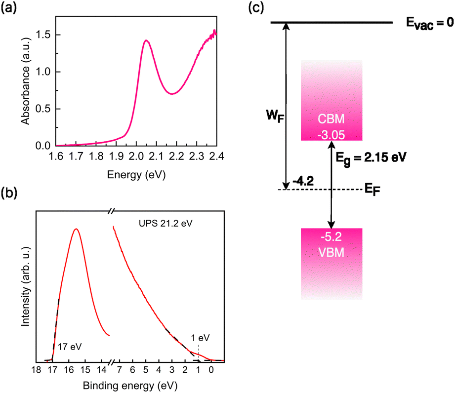 | ||
| Fig. 3 (a) The absorption spectrum of the 300 nm TMA2SnI4 layer deposited on glass. (b) UPS spectra of TMA2SnI4. The secondary electron edge and the valence band maximum position were identified as 17 eV and 1 eV, respectively, and are labelled on the spectrum. (c) The band diagram for TMA2SnI4 obtained from absorption and UPS measurements. | ||
3.3. TMA2SnI4/GaN interface
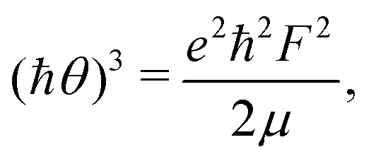
CER is a modulation spectroscopy technique that relies on a perturbation of materials dielectric function through altering the near-surface band bending by the externally applied electric field. This results in the emergence of resonant-like features in the modulated reflectance spectrum around energies corresponding to optical transitions.22,30 For structures with the built-in electric field, Franz–Keldysh Oscillations (FKO) appear in the modulated reflectance spectrum at the energies above the fundamental transition of the analyzed structure. The strength of this built-in electric field is associated with the FKO period and can be determined from:31,32 | (1) |
 | (2) |
 | (3) |
In van Hoof structures, the built-in electric field arises in the undoped top layer as a consequence of the difference of the Fermi level position at the surface and at the interface of a highly doped/undoped layer.33 At the interface between the doped and undoped GaN, the Fermi level is situated near the conduction band edge (CB) or the valence band edge (VB) due to n-type or p-type doping, respectively. Conversely, on the opposite side of the undoped layer, the surface Fermi level position is anchored by surface states to one of the two densities of states (SDOS) within the GaN band gap. Their existence is attributed to the presence of Ga dangling bonds on the GaN surface.34 For the polar GaN surface with the 2 × 2 GaT4 surface reconstruction, it was proven theoretically35 and experimentally33 that the upper SDOS (US), extending approximately 0.6 eV from the conduction band edge into the GaN bandgap, determines the surface Fermi level for n-doped structures. Conversely, the lower SDOS (LS) is situated approximately 1.7 eV from the CBE, nearly at the midpoint of the GaN bandgap, and establishes the surface Fermi level for p-doped structures. The electric field built-in the top layer of van Hoof structures gives rise to the FKO in the modulated reflectance spectrum. Its value can be calculated according to eqn (2) and (3). For n-type van Hoof structures (GaN:Si) at room temperature, all dopants are already ionizied36 and the depletion layer between the undoped cap and the doped layer is sufficiently small to allow for the calculation of the surface barrier from:
| Φn = Fd. | (4) |
In this work, a series of TMA2SnI4/GaN hybrids together with reference GaN structures with undoped GaN layers of 40, 60, and 80 nm thicknesses for Si doped (n-type) substrates, and a 60 nm thickness for Mg doped (p-type) substrates were examined. The upper panels of Fig. 4(a) and (b) display CER spectra acquired for n-type van Hoof structures with a 40 nm thick undoped layer and p-type GaN structure, respectively. In both cases, TMA2SnI4/GaN hybrids together with reference GaN samples were investigated. In all spectra, a resonance corresponding to the GaN bandgap transition at 3.45 eV is observed, accompanied by the Franz–Keldysh oscillation (numbered) above it. As evident, the FKO period for TMA2SnI4 covered samples varies from that observed for reference GaN. For TMA2SnI4/GaN:Si hybrids (Fig. 4(a)), the FKO period is reduced compared to the reference GaN, while for TMA2SnI4/GaN:Mg samples (Fig. 4(b)) the opposite relationship is observed: the FKO period is increased, which points to the change in the value of the built-in electric field in the presence of TMA2SnI4. Such a relationship is supported by the analysis conducted according to eqn (3) and presented in lower panels of Fig. 4(a) and (b). Observably, n-type van Hoof GaN substrates exhibit a decrease of the built-in electric field, whereas p-type van Hoof GaN structures demonstrate an increase in this value. CER spectra and built-in electric field analysis for all investigated n-type and p-type substrates are presented in Fig. S1(a) and S2 in the ESI.† In accordance with eqn 4, the altered value of the built-in electric field indicates a change in the surface barrier height (Φ). These values were computed for both reference GaN substrates and TMA2SnI4 covered hybrids, as illustrated in Fig. 5, with the procedure for obtaining them for n-type structures as shown in Fig. S1(b) and described in the ESI.† As observed, there is a decrease in the surface barrier for electrons from 0.6 eV to 0.5 eV for GaN:Si substrates upon coverage by TMA2SnI4. Conversely, for GaN:Mg, an increase in the surface barrier height for holes from 0.8 eV (for reference) to 0.95 eV (for TMA2SnI4 covered hybrids) is revealed. The change of the surface barrier is related to the unpinning of the surface Fermi level from its native position due to ongoing electronic phenomena.
 | ||
| Fig. 4 CER spectra of reference GaN and TMA2SnI4/GaN hybrids for (a) n-GaN with the 40 nm undoped cap layer and (b) p-GaN with the 60 nm undoped cap layer. Lower panels in (a) and (b) present an evaluation of the built-in electric field. | ||
 | ||
| Fig. 5 The surface barrier calculated for GaN and TMA2SnI4/GaN hybrids. | ||
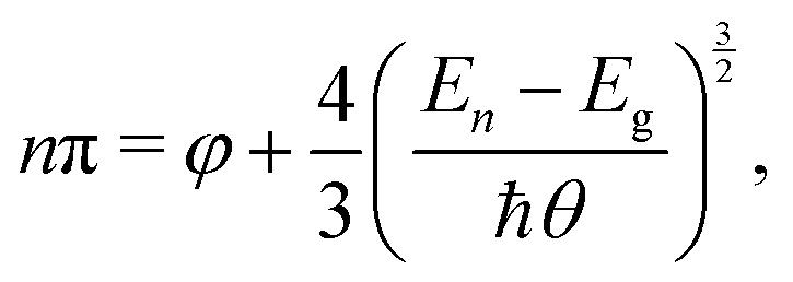
Fig. 6(a) and (b) show the scheme of the GaN band bending (black solid lines) and band edges of TMA2SnI4 (in pink) and GaN (in blue). Orange lines represent GaN surface densities of states. Black dashed lines mark the Fermi level in GaN and TMA2SnI4. The illustrated alignment of Fermi levels at the perovskite/GaN interface represents the state before equilibrium is reached. The conduction band minimum (CBM) in GaN is situated at an energy of approximately −3.25 eV,37 which is 0.2 eV below the CBM of TMA2SnI4 (−3.05 eV), as extracted from UPS measurements (refer to Fig. 3). Consequently, electrons from the conduction band of TMA2SnI4 flow to the GaN surface. This results in an upward shift of the surface Fermi level in GaN (indicated by the red arrow in Fig. 6(a)) and a decrease in the surface barrier Φn, which is consistent with CER results (see Fig. 5).
 | ||
| Fig. 6 (a) Sketch of GaN band bending and the TMA2SnI4/GaN band alignment versus the vacuum level for (a) TMA2SnI4/GaN:Si and (b) TMA2SnI4/GaN:Mg structures. (c) Band alignment at the TMA2SnI4/GaN interface. Arrows show the direction of carriers flow. | ||
From UPS experiments on TMA2SnI4, the VBM was determined to be −5.2 eV. Given that GaN has a larger energy gap (3.45 eV) compared to TMA2SnI4 (2.15 eV), its VBM is positioned 1.5 eV below that of TMA2SnI4. The flow of holes from the GaN surface to TMA2SnI4 occurs leading to the upward shift of the surface Fermi level (Fig. 6(b)) and increase of the surface barrier for holes Φp, as shown in CER (see Fig. 5). This analysis leads to the conclusion that the TMA2SnI4/GaN interface is characterized by the type II band alignment with a conduction band offset of ΔEc = 0.2 eV and a valence band offset of ΔEv = 1.5 eV as illustrated in Fig. 6(c). Such a band alignment is advantageous for use in photodetectors38 and neuromorphic devices such as photonic synapses.19 Since natural synapses integrate computing and memory functions,19 it is believed that developing hardware and software inspired by them will help overcome the bottleneck effect in the von Neumann architecture, which arises from the separation of computing and memory units.19 Consequently, a significant increase in computing capabilities and more efficient energy utilization could be achieved. Reported realizations of photonic synapses are based on III–V semiconductors39 or 2D materials including transition metal dichalcogenides, graphene, hexagonal boron nitride and black phosphorus.19 Perovskites have also been successfully integrated into the active area of such devices.40,41 The coexistence of ionic motion and electronic conduction, coupled with facile solution-based fabrication, is beneficial for achieving modulatable hysteretic operation of the synapses and for future scaling up from single device to arrays.41 Furthermore, implementation of GaN/AlGaN and (PEA)2PbI4 in high electron mobility transistors for neuromorphic vision sensors has been successfully demonstrated.42 This indicates that the investigated interface between GaN and the Pb-free 2D perovskite TMA2SnI4 could be considered as a candidate for the active area in neuromorphic devices.
4. Conclusions
In this work, an interface of TMA2SnI4 – a representative of the Pb-free 2D HOIP – and GaN was investigated. Carriers flowing through the TMA2SnI4/GaN interface were examined by CER spectroscopy and the band edge positions of TMA2SnI4 relative to the vacuum level were revealed by UPS experiments. It was shown that in the presence of TMA2SnI4 the surface Fermi level of GaN is shifted upward, which is translated to the reduction of the surface barrier for electrons and its increase for holes. We correlate it with the electron transfer from TMA2SnI4 to GaN and hole transfer in the opposite direction. This observation is consistent with UPS results showing that the investigated TMA2SnI4/GaN interface exhibits a type II band alignment with the VBO and CBO values of 1.5 eV and 0.2 eV, respectively. With these findings, we draw conclusions about the possible application of such heterojunctions in photodetectors and emerging energy-saving optoelectronic devices as photonic synapses or optical memory systems.Author contributions
E. Z.: investigation, formal analysis, writing – original draft, and project administration; Ł. P.: resources and investigation; W. Ż.: investigation; M. G.: investigation; M. C.: resources and investigation; C. S.: resources and investigation; A. P. H.: investigation, validation and writing – review and editing; R. K.: supervision.Data availability
Data for this paper, including raw data and processed data, are available at Zenodo at https://doi.org/10.5281/zenodo.12820128.Conflicts of interest
There are no conflicts to declare.Acknowledgements
This work was supported by the National Science Centre (NCN) in Poland through grants Preludium-21 no. 2022/45/N/ST3/03465 and Opus grant no. 2020/39/B/ST3/02704. E. Z. was also supported by the Foundation for Polish Science (FNP).References
- E. Halper, The Washington Post, March 2024, Amid explosive demand, America is running out of power, https://www.washingtonpost.com/business/2024/03/07/ai-data-centers-power/, access 4.04.2024.
- M. Rahimi Azghadi, Y.-C. Chen, J. K. Eshraghian, J. Chen, C.-Y. Lin, A. Amirsoleimani, A. Mehonic, A. J. Kenyon, B. Fowler, J. C. Lee and Y.-F. Chang, Adv. Intell. Syst., 2020, 2, 1900189 CrossRef.
- M. Koot and F. Wijnhoven, Appl. Energy, 2021, 291, 116798 CrossRef.
- K. Hoo Teo, Y. Zhang, N. Chowdhury, S. Rakheja, R. Ma, Q. Xie, E. Yagyu, K. Yamanaka, K. Li and T. Palacios, J. Appl. Phys., 2021, 130, 160902 CrossRef CAS.
- S. Olaleru, J. Kirui, D. Wamwangi, K. Roro and B. Mwakikunga, Sol. Energy, 2020, 196, 295–309 CrossRef CAS.
- Y. Xing, H. He, Z. Cui, Z. Fu, S. Qin, W. Zhang, S. Mei and R. Guo, Adv. Opt. Mater., 2024, 12, 2302679 CrossRef CAS.
- K. Chen, Q. Zhang, Y. Liang, J. Song, C. Li, S. Chen, F. Li and Q. Zhang, Front. Phys., 2023, 19, 23502 CrossRef.
- F. Liu, R. Wu, J. Wei, W. Nie, A. D. Mohite, S. Brovelli, L. Manna and H. Li, ACS Energy Lett., 2022, 7, 1066–1085 CrossRef CAS.
- K. Sakhatskyi, B. Turedi, G. J. Matt, E. Wu, A. Sakhatska, V. Bartosh, M. N. Lintangpradipto, R. Naphade, I. Shorubalko, O. F. Mohammed, S. Yakunin, O. M. Bakr and M. V. Kovalenko, Nat. Photonics, 2023, 17, 510–517 CrossRef CAS.
- L. Mao, C. C. Stoumpos and M. G. Kanatzidis, J. Am. Chem. Soc., 2019, 141, 1171–1190 CrossRef CAS PubMed.
- Y.-T. Li, L. Han, H. Liu, K. Sun, D. Luo, X.-L. Guo, D.-L. Yu and T.-L. Ren, ACS Appl. Electron. Mater., 2022, 4, 547–567 CrossRef CAS.
- G. Vescio, D. N. Dirin, S. González-Torres, J. Sanchez-Diaz, R. Vidal, I. P. Franco, S. D. Adhikari, V. S. Chirvony, J. P. Martínez-Pastor, F. A. Vinocour Pacheco, L. Przypis, S. Öz, S. Hernández, A. Cirera, I. Mora-Seró, M. V. Kovalenko and B. Garrido, Adv. Sustainable Syst., 2024, 2400060 CrossRef CAS.
- H. P. Adl, J. Sánchez-Díaz, G. Vescio, A. Cirera, B. Garrido, F. A. V. Pacheco, W. Żuraw Przypis, S. Öz, I. Mora-Seró, J. P. Martínez-Pastor and I. Suárez, Adv. Mater., 2024, 36, 2313252 CrossRef CAS PubMed.
- G. Li, Y. Wang, L. Huang and W. Sun, ACS Appl. Electron. Mater., 2022, 4, 1485–1505 CrossRef CAS.
- F. Cao and L. Li, Adv. Funct. Mater., 2021, 31, 2008275 CrossRef CAS.
- K. J. Lee, J.-W. Min, B. Turedi, A. Y. Alsalloum, J.-H. Min, Y. J. Kim, Y. J. Yoo, S. Oh, N. Cho, R. C. Subedi, S. Mitra, S. E. Yoon, J. H. Kim, K. Park, T.-H. Chung, S. H. Jung, J. H. Baek, Y. M. Song, I. S. Roqan, T. K. Ng, B. S. Ooi and O. M. Bakr, ACS Energy Lett., 2020, 5, 3295–3303 CrossRef CAS.
- Z.-T. Li, H.-W. Zhang, J.-S. Li, K. Cao, Z. Chen, L. Xu, X.-R. Ding, B.-H. Yu, Y. Tang, J.-Z. Ou, H.-C. Kuo and H.-L. Yip, Adv. Sci., 2022, 9, 2201844 CrossRef CAS PubMed.
- J. Guo, B. Ye, Y. Gu, Y. Liu, X. Yang, F. Xie, X. Zhang, W. Qian, X. Zhang, N. Lu and G. Yang, ACS Appl. Mater. Interfaces, 2023, 15, 56014–56021 CrossRef CAS PubMed.
- S. Wang, C. Chen, Z. Yu, Y. He, X. Chen, Q. Wan, Y. Shi, D. W. Zhang, H. Zhou, X. Wang and P. Zhou, Adv. Mater., 2019, 31, 1806227 CrossRef PubMed.
- E. Zdanowicz, A. P. Herman, Ż. Przypis, K. Opołczyńska, J. Serafińczuk, M. Chlipała, C. Skierbiszewski and R. Kudrawiec, Phys. Chem. Chem. Phys., 2023, 25, 16492–16498 RSC.
- W. Żuraw, D. Kubicki, R. Kudrawiec and Ł. Przypis, ACS Energy Lett., 2024, 4509–4515 CrossRef PubMed.
- E. Zdanowicz, A. P. Herman and R. Kudrawiec, Appl. Surf. Sci., 2022, 577, 151905 CrossRef CAS.
- M.-H. Jung, Dalton Trans., 2021, 50, 10261–10274 RSC.
- A. P. Herman, L. Janicki, H. S. Stokowski, M. Rudzinski, E. Rozbiegala, M. Sobanska, Z. R. Zytkiewicz and R. Kudrawiec, Adv. Mater. Interfaces, 2020, 7, 2001220 CrossRef CAS.
- E. Zdanowicz, A. P. Herman, K. Opołczyńska, S. Gorantla, W. Olszewski, J. Serafińczuk, D. Hommel and R. Kudrawiec, ACS Appl. Mater. Interfaces, 2022, 14, 6131–6137 CrossRef CAS PubMed.
- E. Zdanowicz, A. P. Herman, M. Sobanska, Z. R. Zytkiewicz, W. Olszewski, D. Hommel and R. Kudrawiec, ACS Appl. Electron. Mater., 2022, 4, 5017–5025 CrossRef CAS.
- Ł. Janicki, J. Misiewicz, M. Siekacz, H. Turski, J. Moneta, S. Gorantla, C. Skierbiszewski and R. Kudrawiec, Sens. Actuators, B, 2019, 281, 561–567 CrossRef.
- K. R. Hansen, C. E. McClure, D. Powell, H.-C. Hsieh, L. Flannery, K. Garden, E. J. Miller, D. J. King, S. Sainio, D. Nordlund, J. S. Colton and L. Whittaker-Brooks, Adv. Opt. Mater., 2022, 10, 2102698 CrossRef CAS.
- M.-C. Tang, S. Zhang, T. J. Magnanelli, N. V. Nguyen, E. J. Heilweil, T. D. Anthopoulos and C. A. Hacker, Mater. Adv., 2021, 2, 1253–1262 RSC.
- F. H. Pollak and H. Shen, Mater. Sci. Eng., R, 1993, 10, 374 CrossRef.
- X. Yin and F. H. Pollak, Appl. Phys. Lett., 1991, 59, 2305–2307 CrossRef CAS.
- D. E. Aspnes and A. A. Studna, Phys. Rev. B: Solid State, 1973, 7, 4605–4625 CrossRef CAS.
- Ł. Janicki, M. Gładysiewicz, J. Misiewicz, K. Klosek, M. Sobanska, P. Kempisty, Z. R. Zytkiewicz and R. Kudrawiec, Appl. Surf. Sci., 2017, 396, 1657–1666 CrossRef.
- C. G. Van de Walle and D. Segev, J. Appl. Phys., 2007, 101, 081704 CrossRef.
- D. Segev and C. G. Van de Walle, J. Cryst. Growth, 2007, 300, 199–203 CrossRef CAS.
- P. Bogusławski and J. Bernholc, Phys. Rev. B: Solid State, 1997, 56, 9496–9505 CrossRef.
- Z. Zhang, Q. Qian, B. Li and K. J. Chen, ACS Appl. Mater. Interfaces, 2018, 10, 17419–17426 CrossRef CAS PubMed.
- C. Lin, P. Wan, B. Yang, D. Shi, C. Kan and M. Jiang, J. Mater. Chem. C, 2023, 11, 12968–12980 RSC.
- D. Sarkar, J. Tao, W. Wang, Q. Lin, M. Yeung, C. Ren and R. Kapadia, ACS Nano, 2018, 12, 1656–1663 CrossRef CAS PubMed.
- H. Tian, L. Zhao, X. Wang, Y.-W. Yeh, N. Yao, B. P. Rand and T.-L. Ren, ACS Nano, 2017, 11, 12247–12256 CrossRef CAS PubMed.
- S. K. Vishwanath, B. Febriansyah, S. E. Ng, T. Das, J. Acharya, R. A. John, D. Sharma, P. A. Dananjaya, M. Jagadeeswararao, N. Tiwari, M. R. C. Kulkarni, W. S. Lew, S. Chakraborty, A. Basu and N. Mathews, Mater. Horiz., 2024, 11, 2643–2656 RSC.
- X. Hong, Y. Huang, Q. Tian, S. Zhang, C. Liu, L. Wang, K. Zhang, J. Sun, L. Liao and X. Zou, Adv. Sci., 2022, 9, 2202019 CrossRef CAS PubMed.
Footnote |
| † Electronic supplementary information (ESI) available: CER spectra for all investigated samples; XPS and PL of TMA2SnI4; TRPL of TMA2SnI4/glass and TMA2SnI4/GaN samples. See DOI: https://doi.org/10.1039/d4tc03203a |
| This journal is © The Royal Society of Chemistry 2024 |