
 Open Access Article
 This Open Access Article is licensed under a
 Creative Commons Attribution 3.0 Unported Licence
Optoelectronic characteristics of furan substituted thiophene/phenylene co-oligomer single crystals for organic lasing†
Periyasamy Angamuthu
Praveen
 *a,
Thangavel
Kanagasekaran
*b,
Chaoyan
Ma
c,
Masahiro
Terada
c,
Tienan
Jin
d,
Yusuke
Wakabayashi
a and
Hidekazu
Shimotani
*a
*a,
Thangavel
Kanagasekaran
*b,
Chaoyan
Ma
c,
Masahiro
Terada
c,
Tienan
Jin
d,
Yusuke
Wakabayashi
a and
Hidekazu
Shimotani
*a
aDepartment of Physics, Graduate School of Science, Tohoku University, Sendai, Japan. E-mail: praveen@tohoku.ac.jp; shimotani@tohoku.ac.jp
bOrganic Optoelectronics Laboratory, Department of Physics, Indian Institute of Science Education and Research – Tirupati, Tirupati, India. E-mail: kanagasekaran@iisertirupati.ac.in
cDepartment of Chemistry, Graduate School of Science, Tohoku University, Sendai, Japan
dResearch and Analytical Center for Giant Molecules, Graduate School of Science, Tohoku University, Sendai, Japan
First published on 30th August 2024
Abstract
We design and synthesise an organic lasing system, 2,5-bis(5-[1,1′-biphenyl]-4-ylthiophen-2-yl)furan, which has advanced optoelectronic properties. Grown as a single crystal, this monoclinic system exhibits typical H-aggregation and has a photoluminescence quantum yield of 29% and ambipolar field effect mobilities of approximately 0.7 (hole) and 0.1 (electron) cm2 V−1 s−1. The system is validated for its suitability towards laser development, and it exhibits excellent gain along with dual gain-narrowing emission in the yellow region. It has superior optical and electrical properties compared to its structural counterpart and similar systems. The system can be further developed by incorporating a planar resonator structure and using contact engineering techniques to realise electrically driven semiconductor lasers.
Introduction
A fundamental issue in realising electrically pumped solid-state organic lasers is the limited availability of materials. For efficient lasing, a material should have high mobility and high photoluminescence quantum yield (PLQY). However, such materials are scarce in organic semiconductors (OSC) due to their inherent π–π stacking, which results in good mobility but also induces severe exciton quenching, leading to poor emission.1 The best practical way is therefore to identify systems with moderate mobilities and moderate PLQYs. Due to such limitations, only a few systems are demonstrated to be suitable for organic lasing.2So far, three materials, such as 5,5′-bis(4-biphenylyl)-2,2′:5',2′-terthiophene (BP3T), 4,4′-bis[(N-carbazole) styryl]biphenyl and a combination of 2,7-bis(9,9-spirobifluoren-2-yl)-9,9-spirobi-fluorene and poly(2,5-bis-(2′,5′-bis(2′-ethylhexyloxy)phenyl)-p-phenylene vinylene) are shown to have the possibility of realising electrically driven lasers.3–5 Of these three, BP3T-based organic light-emitting transistor (OLET) has the simplest device architecture with emission in the yellow region. However, BP3T suffers from several issues, such as low stability, short operation times and the occurrence of singlet–triplet annihilation.5 One way to improve the optoelectronic properties of BP3T is by substituting furan core in the place of thiophene.6,7
Furan is the oxygen analogue of thiophene and holds great promise for optoelectronic applications. Due to the smaller atomic size of oxygen than sulphur, the moiety would induce a smaller steric hindrance effect results small torsional angles and better molecular planarity.8 Furthermore, unlike thiophene, furan does not suffer from the heavy atom effect. Compared with sulphur, oxygen has a smaller covalent radius and higher electronegativity which will shorten the π–π stacking distance and tune frontier orbitals and charge transport in furan based OSCs.9 These systems have strong fluorescence, which is beneficial for lasing-related applications.10–12
In the present work, we have substituted the furan into one of the rings of BP3T to obtain a new derivative: 2,5-bis(5-[1,1′-biphenyl]-4-ylthiophen-2-yl)furan (BPTFT). Its structural, optical, electronic and lasing characteristics are reported. The single crystals (SCs) of BPTFT are demonstrated to exhibit optically pumped Fabry–Pérrot (FP) lasing and have a threshold value of approximately 20 μJ cm−1 in the 560 nm region. We have also observed dual gain-narrowing in BPTFT, a signature phenomenon in biphenylyl/thiophene systems and found that it varies according to crystal thickness. Electrically pumped organic lasing can be realised in either diode or transistor architectures. However, due to their lateral geometry and the availability of gate insulators, OLETs are better than diodes, offering higher efficiency and lower optical loss. In this study, we have investigated the suitability of BPTFT for electrically pumped lasing by constructing its SC as an OLET. It shows ambipolar charge transport with hole and electron mobilities of 0.7, 0.1 cm2 V−1 s−1, respectively. With this, the inclusion of a resonator structure and proper contact engineering will make BPTFT OLETs an ideal candidate for developing yellow-emitting electrically pumped organic lasers.
Results and discussion
Synthesis of BPTFT
First, 2-(5-(biphenyl-4-yl)thiophen-2-yl)-5-bromofuran (S1a, 5.0 mmol, 1.9 g), (5-(biphenyl-4-yl)thiophen-2-yl)boronic acid (S1b, 7.5 mmol, 2.1 g), Pd(PPh3)4 (0.25 mmol, 289 mg), Na2CO3 (25 mmol, 2.65 g) were added to a mixture of THF and H2 O (v/v = 2/1, 0.1 M, 50 mL) under N2 atmosphere (Fig. 1). Then, the reaction mixture was stirred for 48 h at 80 °C and filtered by washing with water, MeOH, and CH2Cl2. The residue was further heated in CHCl3 at 80 °C and filtered while hot. The resulting green solid was further recrystallised in 1,2,4-trichlorobenzene at 180 °C (0.5 h) to produce BPTFT (yellow solid, 2.1 g, 79% yield). Anal. calcd for C36H24OS2: C, 80.56; H, 4.51; S, 11.95; found: C, 80.61; H, 4.58; S, 12.04%. The resulting BPTFT was purified via vacuum sublimation (∼5 × 10⁻³ Pa for more than 80 h) twice to obtain the material for crystal growth.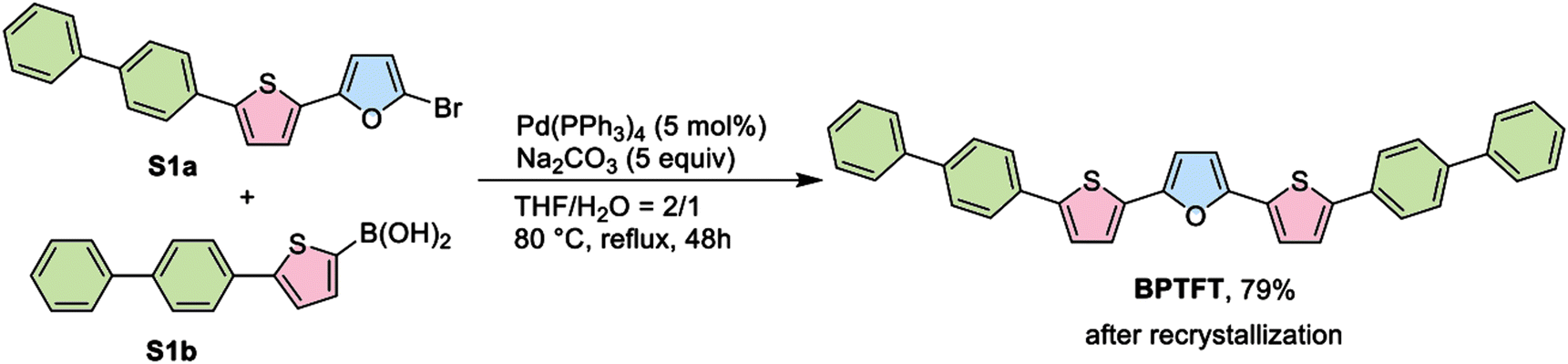 | ||
| Fig. 1 Synthesis scheme for BPTFT. | ||
Structural analysis
BPTFT SCs were grown through physical vapour transport (PVT; Experiments section) and subjected to X-ray diffraction analysis. Similar to its parent system (BP3T), BPTFT crystallises in a monoclinic system with a space group P21c. Its lattice parameters are a = 7.48 Å, b = 5.63 Å, c = 59.16 Å, β = 90.97°, Z = 4 and V = 2495 Å3. The refined crystallographic information was deposited with the Cambridge Crystallographic Data Centre (CCDC 2365344†), and the packing structure is given in Fig. 2(a–d). Compared to BP3T (a = 7.52 Å, b = 5.78 Å, c = 59.09 Å, β = 92.81° and V = 2609 Å3) the volume is slightly reduced for BPTFT.13 The molecules are H-aggregated and stacked in a parallel, face-to-face fashion, which is favourable for optoelectronic applications. A photomicrograph of a PVT-grown BPTFT SC under UV irradiation and the refined morphology using WinXmorph program14 are given in Fig. 2(e and f). The morphology of PVT-grown crystals is similar to the theoretically simulated features. At the molecular level, the bond between the central furan ring and the side chain thiophene rings in BPTFT is slightly shorter by 0.02 Å than the thiophene-thiophene bond in BP3T. The dihedral angle in BPTFT is also 3° lower than that in the BP3T system. Furthermore, the orientation of the molecular long axis in BP3T is slightly tilted 2.6° normal to the ab-plane.13 Conversely, BPTFT is oriented perfectly perpendicular to the bottom plane, which is ideal for photon confinement within the cavity. Such variation can be attributed to the furan substitution, which has shorter O–C bond and a rigid structure, resulting in tighter packing in the unit cell. In addition, the furan substitution has significantly altered the molecular planarity. | ||
| Fig. 2 Crystal structure of BPTFT. Projections on (a) bc (b) abc (c) ab (d) ac planes. (e) PVT grown and (f) simulated morphology of BPTFT SC. | ||
In an ideal planar system, the planarity indices, molecular planarity parameter (MPP) and span of deviation from the plane (SDP) are equal to zero (Experiments section). The calculated MPP and SDP for BPTFT are 0.13 and 0.48 Å, respectively. These values are half of those of BP3T, which are 0.26 and 1.06 Å, respectively, indicating that BPTFT is structurally more planar than BP3T. Gas phase density functional theory (DFT) simulation reproduces the trend with higher planarity indices (Section S1 and Fig. S1, ESI†) primarily due to the absence of intermolecular forces and symmetry constraints. Planarity maps of BPTFT and BP3T are given in Fig. 3(a) and (b), respectively. The blue and red regions indicate the fragment deviation in positive and negative directions, respectively, concerning the fitting plane (white). Despite a slight bend between the furan and one of the thiophene cores, the inclusion of furan generally improves molecular planarity. This often occurs in furan substitution due to the small torsional angles with the inclusion of oxygen and results in better rigidity. This molecular feature reduces the spacing between oligomeric rings in the solid state and is beneficial for light emission and charge transport.15–17
 | ||
| Fig. 3 Molecular planarity plots of (a) BPTFT and (b) BP3T, which have the MPP of 0.13, 0.26 Å and SDP of 0.48 and 1.06 Å, respectively. (c) TDM orientation of BPTFT. (d) PL intensity as a function of incident laser polarisation angle at 560 nm for BPTFT SC. | ||
The theoretically calculated transition dipole moment (TDM) vector is depicted in Fig. 3(c). The dominant dipole moment, corresponding to the S1 → S0 state, is oriented along the molecular long axis. As the molecules are arranged perpendicular to the ab-plane, the TDM is also aligned perpendicular to that plane and light emission can be obtained at the crystal edges.18 This is advantageous for optical confinement and indicates that the crystalline cavity can simultaneously act as a gain medium and an optical resonator, desirable for organic lasing. The maximum emission intensity was obtained from the (1 0 0) plane and indicates that the TDMs are aligned horizontally along the width direction, in line with the theoretical results. The polarization-dependent photoluminescence (PL) performance of a BPTFT SC (Experiments section) is given in Fig. 3(d). Furthermore, the degree of linear polarisation (DOLP) was calculated as, DOLP = (Imax − Imin)/(Imax + Imin), where Imax and Imin are the maximum and minimum intensities of the light emission, respectively.19 For BPTFT, the DOLP value is 0.49. For comparison, a BP3T SC of a similar thickness was used. Its DOLP value (0.27) is nearly half of that of BPTFT, indicating superior intrinsic polarised emission from BPTFT.
Excited state analysis
The photophysical properties of BPTFT were investigated at the experimental and theoretical levels. Fig. 4 shows the recorded absorption, fluorescence and photoelectron yield spectrum (PYS) of BPTFT along with the frontier molecular orbitals, the four-level energy model for the emission process and the Commission Internationale deI'Eclairage (CIE) coordinates of the emission profiles of the BPTFT system. The highest occupied molecular orbital (HOMO) level determined using the PYS is EHOMO = −5.10 eV. The optical band gap (Eopt) of BPTFT was determined to be 2.28 eV using a Tauc plot (Fig. S2, ESI†). The exciton binding energies were estimated as Δex = Eopt/3 = 0.76 eV.20,21 Therefore, the lowest unoccupied molecular orbital (LUMO) level is ELUMO = EHOMO + Eopt + Δex = −2.06 eV. Although two transitions (HOMO → LUMO and HOMO−1 → LUMO+1) contribute to the S0 → S1 transition, most of the contribution (∼91%) is from the frontier molecular orbitals. The corresponding EHOMO, ELUMO, Eopt and Δex values of BP3T are −5.78, −2.64, 2.38 and 0.79 eV, respectively.22 BPTFT has a lower ionisation potential than BP3T. This is advantageous from a contact engineering perspective as it matches the work function of gold and will significantly reduce the charge injection barrier for hole injection. | ||
| Fig. 4 Photophysical process in BPTFT. (a) Four-level energy model with DFT-calculated frontier molecular orbitals; H and L represent HOMO and LUMO, respectively. (b) PYS spectrum and (c) normalised absorption and PL spectra. Inset: CIE 1931 coordinates of BPTFT SC. | ||
The BPTFT absorption spectrum can be resolved into three prominent peaks corresponding to 0 → 0, 0 → 1 and 0 → 2 transitions. In H-aggregates, 0 → 0 band is forbidden or weakened due to Davydov splitting and the emission bands in the PL spectrum are assigned to higher-order transitions (0 → 1, 0 → 2 and 0 → 3). The emission bands at 560 and 590 nm are assigned to the CIE coordinates (0.37, 0.62) and (0.57, 0.42), respectively. The external PLQY obtained for BPTFT is approximately 29%. BP3T assessed using a similar method, exhibits a PLQY of only 24%, indicating the superior optical properties of BPTFT over BP3T.
The Strickler–Berg relation (Sections S3 and S4, ESI†) was used to calculate the fluorescence lifetime and fluorescence rate constant, which are 0.9 ns and 3 × 10⁸ s−1, respectively.23 Such a short radiative decay time and high rate constant indicate the possibility of stimulated emission (SE) in the band, in an order similar to that of other reported systems.24,25 For further confirmation, we theoretically calculated the fluorescence rate in the singlet state (S1) at PBE/def2-SVP level. The obtained value is 2.5 × 10¹⁰ s−1, which is one order higher than that for BP3T (4.9 × 10⁹ s−1). In OSCs, both Franck–Condon (FC) and Herzberg–Teller (HT) states contribute to the emission. In the case of BP3T, the FC contribution is 10.3%, and the HT contribution is 89.7%. As for BPTFT, only 2% of emission arises due to FC and a major 98% was contributed by HT, indicate the presence of strong vibrational coupling in the system.
Hole–electron distribution analysis was carried out to obtain further insights into the excitation dynamics in BPTFT.26,27 As most organic luminescent systems follow Kasha's rule, most of the luminescence arises from the S1 state. This process can be modeled using a four-level energy transfer process as depicted in Fig. 4(a). Upon excitation from the ground state to the excited state, the electron vibrationally relaxes non-radiatively to a low-lying excited state. Thus, the S0 → S1 transitions were analysed to describe the excitation process. The hole–electron distribution plots and the fragment distribution heatmap for S0 → S1 transitions are given in Fig. 5. Contributions to the excitation process from the other states such as S4, S6 and S7 are also evident (Fig. S3, ESI†). However, their contribution is minimal. As shown in Fig. 5, the excitation process is due to the local excitons, i.e., both the hole and electron occupy spatially similar regions. Moreover, in both cases, most of the contributions arise from the thiophene/furan cores rather than the phenylyl rings. Both sulphur and oxygen contribute to electron distribution, however, the furan contribution is slightly lower than that of its structural counterpart, which would impact the charge transport. On the contrary, with better molecular rigidity, BPTFT would have better emission profiles than BP3T. This can be envisaged using oscillator strengths and charge transfer lengths, as BPTFT has slightly higher values (2.94 and 0.06 Å) than BP3T (2.86 and 0.05 Å). This explains the higher PLQY values obtained for BPTFT than the BP3T. It should be noted that the above conclusions are obtained from the molecular perspective. Nevertheless, the intermolecular interaction should have a definite role in both emission and charge transfer mechanisms. A separate work is required to explore this further.
 | ||
| Fig. 5 Hole–electron distributions of (a) BPTFT and (b) BP3T. The heatmap (a.u.) depicts the molecular fragment contribution, where Bn denotes phenyls, Tn denotes thiophenes and F1 denotes furan. | ||
Lasing characteristics
In BPTFT, the TDMs are arranged along the molecular long axis, so light is confined within the cavity and emitted through the edges. The parallel faces of the crystal act as a natural FP resonator. At a low excitation energy, BPTFT exhibits a broadband emission spectrum. At energies exceeding 20 μJ cm−2, the 560 nm emission peak narrows as shown in Fig. 6(a). With a further increase in excitation power, the emission intensity increases sharply, with a rapid reduction in the emission profile's full-width at half-maximum (FWHM). This behaviour indicates the onset of amplified spontaneous emission, with the threshold being approximately 20 μJ cm−2 (Table 1). Beyond this threshold, the FWHM value reduces by only 0.7 nm, which fits well with the Schawlow–Townes formula. The calculated net gain coefficient (g) (Fig. 6(d)) is 42 cm−1 at an excitation density of 37.6 μJ cm−2 (Fig. S4(b), ESI† and Experiments section). The calculated loss coefficient (k) (Fig. 6(f)) is 16 cm−1, attributed to the waveguide and self-absorption losses in the medium. The obtained optical gain is related to the SE cross-section (σ) in that g = σ(λ)N, where N is the population inversion density. The calculated σ(λ) value is 2.37 × 10⁻¹⁶ cm2 (Section S7, ESI†). This value is quite close to those of similar lasing systems, suggesting the potential of further development of BPTFT as a lasing medium.28 | ||
| Fig. 6 Lasing characteristics of BPTFT. (a) Gain narrowing of 0–1 band of crystal with thickness ∼350 nm (the unfilled and filled circles are FWHM and peak intensity, respectively). (b) Dual gain narrowing in crystal with thickness ∼700 nm (the circles and squares are 0–1 and 0–2 bands, respectively). (c) Emission from BPTFT SC at 36.6 μJ cm−2 of input intensity. (d) Dependence of output light intensity on excitation beam length; g denotes the net gain coefficient at input intensities of (from left to right) 26.6, 31.6 and 37.6 μJ cm−2, respectively. (e) Input intensity dependence of emission spectra with 0–1 and 0–2 emission bands for crystal with thickness of ∼590 nm. (f) Loss coefficient plot. (g) Laser spectra obtained using high-resolution grating (1800 lines per mm) of BPTFT SCs with cavity lengths (Lr) of approximately (from left to right) 200, 300, and 500 mm. (h) Lr-dependent mode spacing (ΔλL). | ||
| System | PLQY | Threshold | μ h | μ e | Ref. |
|---|---|---|---|---|---|
| a Present work. b Internal quantum efficiency. | |||||
| BPTFT | 0.28 | 20 | 0.7 | 0.1 | |
| BP1T-CN | NA | 53 | 5.70 × 10⁻⁴ | 1.66 × 10⁻³ | 29 |
| BP2T-CN | 0.63 | 176 | — | — | 30 |
| BP4T | NA | 81, 30 | — | — | 31 |
| LD-1 | 0.8 | 86 | 0.25 | — | 32 |
| BP3T-OMe | NA | 17 | — | — | 22 |
| BP3T-CN | NA | 152 | — | — | 22 |
| BP1T | 0.2 | — | 0.01 | — | 33 |
| BP2T | 0.38 | — | 0.08 | 0.011 | 33 |
| BP3T | 0.8b | 40 | 1 | 0.5 | 33 and 34 |
Similar to many other organic lasing systems, BPTFT exhibits dual-wavelength emission characteristics. In this case, such phenomena depend on the thickness of the BPTFT cavity (Fig. S5, ESI†). Of the two emission bands, the 0–1 peak generally gain-narrows upon the increment in pump fluence. The 0–2 peak tends to exhibit gain narrowing, depending on cavity thickness. Fig. 6(a) and (b) show the gain-narrowing characteristics of two BPTFT SCs with thicknesses of below and above 500 nm. For thicknesses of less than 500 nm, only the 0–1 peak exhibits gain narrowing (with a minimal contribution from 0–2 in some cases; Fig. S6(a), ESI†). As the crystal thickness approaches ∼700 nm, both peaks tend to exhibit gain narrowing (Fig. 6(b) and (e)). In some cases, for thicknesses of approximately 1 μm, only the 0–2 peak gain narrows (Fig. S6(b) and (c), ESI†).
The aforementioned four-level energy model was used to analyse these dual-wavelength lasing characteristics. When the ground state (S0) is pumped optically, the absorption leads to an excited state (S1), usually to the E4 level. From E4, it is vibrationally relaxed non-radiatively to the E3 state. From E3, emission is obtained via transition to any of the vibrational levels in E2|0i〉, (i = 1, 2, 3). Due to these transitions in organic systems, lasing can be achieved from any vibronic bands, say 0–1, 0–2 and 0–3. This offers the possibility of tuning the emission wavelength; methods like, thermally induced vibronic switching, excited state proton induced transfer and doping-induced wavelength tuning are already reported for some organic systems.28,35–37 The PL spectrum of BPTFT obtained much below the threshold intensity is shown in Fig. S7 (ESI†), corresponding to four emission bands: 0–1, 0–2, 0–3 and 0–4. The 560 and 595 nm bands are assigned to the 0–1 and 0–2 transitions. Now, the prevailing question of why dual emission occurs can be answered by combining the photophysical properties of BPTFT using this four-level energy model. The calculated lifetime of the 0–2 transition is 0.3 ns, which is somewhat similar to that of the 0–1 transition. Both transitions occupy the same E3 state, so they co-exist. Consequently, upon pumping, both compete for lasing. However, according to Einstein's relation, σ(λ) is directly proportional to absorption and from the theoretical calculations, 0–1 has a higher oscillator strength than the 0–2. In addition, the calculated σ(λ) values are 2.37 × 10⁻¹⁶ and 0.4 × 10⁻¹⁶ cm2 for 0–1 and 0–2 bands, respectively. Hence, the probability for lasing is substantially higher for the 0–1 transition. At thickness lower than the emission wavelength (less than 500 nm), confining the larger wavelength within the cavity is difficult, leading to the strong 0–1 emission.34 With an increase in thickness, 0–1 is significantly dampened by self-absorption, increasing the lasing probability for 0–2.
Resolving the emission spectrum using a high-resolution grating, shows that BPTFT exhibits several distinct peaks, corresponding to the longitudinal modes in the FP cavity. The mode spacing ΔλL values vary with respect to the cavity length (Lr). With an increase in Lr, more peaks tend to appear, as shown in Fig. 6(g). Three Lr values (∼200, 300, and 500 μm) were studied using a high-resolution grating, and the corresponding ΔλL values are 1.1, 0.5 and 0.3 nm, respectively. As seen in Fig. 6(h), the plot of 1/Lrversus ΔλL is linear indicating the presence of the FP resonator along the pump direction.38
The FWHM (Δλ) values of the emission peaks were then used to deduce laser characteristics: quality factors (Q) and coherence lengths (Lc). For BPTFT, the Q-factors of the emission bands were calculated as Q = λ/Δλ, where λ is the emission wavelength of the corresponding peak. Given Δλ values of 1.96 and 2.5, the corresponding Q-factors are ∼300 and ∼250 for 0–1 and 0–2 transitions, respectively. In addition, Lc was calculated using Lc = λ2/2πΔλ, from this temporal coherence was estimated as τc = Lc/c.39,40 For BPTFT, 0–1 and 0–2 transitions have Lc values of 25 and 22 mm, and τc values of 85 and 74 fs, respectively. Although the Q-factor and Lc values are moderate given the dimensions used, the performance decline is attributed to the quality of the natural mirrors at the facet ends. These values can be improved using proper resonator structures, such as distributed feedback resonators for narrower linewidth lasing.
Finally, the stability of the lasing cavity is a crucial parameter in the realisation of organic semiconductor lasers. Although moisture and oxygen often significantly affect performance, BPTFT shows significant stability over constant atmospheric exposure for more than 7 months. The change in threshold and emission intensity is minimal, and a variation of ±2% arises between the measurements at different periods. Such variation may also arise due to the minor variation in sample position, exemplifying the atmospheric stability of BPTFT.
Transistor characteristics
A schematic diagram of the device architecture and the energy levels of different layers are shown in Fig. 7(f) and (g), respectively. The devices are constructed in a bottom-gate, top-contact fashion. The obtained output and transfer curves are given in Fig. 7(a)–(d). The variation in the emission zone with the applied voltage was monitored through a top-mounted microscope. Two operation modes were used for charge transport and electroluminescence analysis. In the transfer curve measurement, the drain voltage (Vd) was kept at 100 V (n-channel) and −120 V (p-channel), and the gate voltage (Vg) varied. In the output curve measurement, Vg was kept constant with an increase in Vd. As seen in Fig. 7(b) and (d), at a low Vg, both hole and electron transport can be achieved, indicating the ambipolar characteristics of BPTFT. | ||
| Fig. 7 Transistor characteristics of BPTFT. (a) Transfer curve (n drive). (b) Output curve (n drive). (c) Transfer curve (p drive). (d) Output curve (p drive). (e) Electrically driven luminescence from BPTFT. (f) Schematic diagram of the OLET. (g) Energy levels of OLET layers. | ||
At a high Vg, the regime transform into a unipolar operation due to charge carrier (hole or electron) trapping with respect to Vg polarity. The mobilities were calculated from the saturation regime (n-drive), and the obtained values are in the range of 0.7 cm2 V−1 s−1 for hole transport and 0.1 cm2 V−1 s−1 for electron transport. The corresponding threshold (Vth) voltages are 60 and 80 V for hole and electron transport, respectively. With Vd and Vg modulation, electrically-driven emission was obtained in the device (Fig. 7(e)). Furthermore, through Vg modulation, the recombination zone can be manipulated which is typically only possible with a transistor device.
Although the obtained mobilities are the highest among recent reports (Table 1), they are slightly lower than those of BP3T. This is essentially due to two factors: reorganisation energies and the charge injection barrier. The DFT-calculated reorganisation energy of BPTFT is 1252 cm−1, which is larger than that of BP3T (1130 cm−1). Thus, the charge transport in BPTFT is slightly lower than that in BP3T. In addition, BPTFT has a larger difference between the electron and hole distributions (Fig. 5) than BP3T. This is one of the reasons why the ratio of hole to electron mobility is larger in BPTFT.
In the present case, we did not use interlayers to modify the charge injection barrier. Contact engineering plays a crucial role in organic semiconducting devices, and depending on the contact type, the material can be operated as a unipolar or ambipolar device. For example, well-known p-type materials, such as tetracene and pentacene have ambipolar characteristics with proper contacts of work functions matching the HOMO and LUMO of the OSC.41,42 In this direction, we introduced novel contact design approaches to obtain the highest current density in rubrene devices.43 However, in the present study, we only intend to demonstrate the ambipolar characteristics of BPTFT; contact design principles are not considered. Tuning the contacts by inserting interlayers may significantly improve mobility. In particular, the obtained results suggest that with suitable resonators and proper contacts, BPTFT will be a potential candidate for the realisation of electrically pumped lasers, a holy grail in organic optoelectronics. Such work deserves a separate treatment and report.
Conclusions
A furan-substituted thiophene/phenylene co-oligomer was synthesised using a coupling reaction. High-quality SCs were grown via PVT, and X-ray diffraction analysis indicated that the system crystallises in a monoclinic form. Compared with its structural counterpart, BP3T, BPTFT has superior optical properties due to the rigidity and conjugation caused by the furan substitution. Their gain-narrowing characteristics indicated that the system has dual gain-narrowing emissions with dominant SE from 0–1 band. The 0–2 band emission can be modified by changing the crystal thickness. The empirically calculated photophysical properties and other optical quantities from optical pumping analysis showed the potential of BPTFT as a lasing cavity. In addition, the ambipolar charge transport in the system was demonstrated by constructing OLETs, and the calculated hole and electron mobilities exceed those in similar systems. However, BPTFT has slightly inferior transport characteristics than BP3T due to the inherent molecular reorganisation energies and device architecture adopted in this work. Still, the obtained mobilities are notable among organic optoelectronic devices. The system can be further improved by integrating an additional resonator into the device's geometry and incorporating contact engineering techniques. Such measures will establish BPTFT as a potential candidate for realising electrically driven organic lasers.Experiments
Crystal growth
The SCs were grown through PVT in an Ar (99.999% purity) stream. A sublimation temperature of 380 °C with a 2.5 °C cm−1 variation in the temperature profile was used for crystal growth. The structure was confirmed using single-crystal X-ray diffraction analysis (Rigaku Oxford Diffraction).Molecular planarity calculations
The molecular structure obtained from the crystallographic studies was analysed, and the implementation available in the Multiwfn module was used to calculate the MPP and SDP.44 A detailed description of the methodology is available elsewhere.45 For the gas phase calculations, optimised geometries were used.DFT analysis
ORCA 5.0.3 was used for the DFT calculations. For geometry optimisation and excited-state calculations, functionals such as B3LYP, CAM-B3LYP, w97X, PBE with basis sets either 6-31G(d,p) or def2-SVP were used. This level of theory is often adequate for modeling the excited states in organic semiconductors.46 Based on the comparison between BP3Ts DFT results with experimental data, CAM-B3LYP data were used for the final discussion. The rate constants and reorganisation energies were calculated using the excited state dynamics (ESD) module with sTDA in ORCA 4.0.2 using the PBE/def2-SVP functional and basis set. The FC and HT contribution values were directly obtained from the ESD output file. Although, hybrid functionals would have produced more accurate results, PBE was selected for rapid testing and identifying differences in trends between BP3T and BPTFT.Polarisation-dependent PL
For the analysis of polarisation-dependent PL, a diode laser with 405 nm wavelength and 5 mW power was irradiated on a SC through a half-wave plate. The emission intensity was collected using a spectrometer (OceanOptics HR2000+). Initially, the (0 0 1) face of the crystal was aligned parallel to the laser polarisation direction. The polarisation angle was gradually varied using the half-wave plate and the corresponding intensity variations were measured.Photophysical properties
The absorption spectrum of BPTFT was recorded using a thin film of thickness 150 nm, deposited by thermal evaporation at a pressure of ∼10−5 Pa. A 405 nm CW diode laser with 5 mW power was irradiated on a BPTFT SC of thickness 500 nm, and the emission spectrum was collected using a spectrometer. The EHOMO values were calculated from (photoelectron yield)0.5 as a function of the incident photon energy measured using PYS (Riken photoelectron yield spectrometer AC-2). The PLQY values were determined using the integrating sphere method (Hamamatsu Photonics C9920-02).Lasing characteristics
A ns pulsed nitrogen laser (Stanford Research Systems NL100), with a 337 nm (13.8 Hz) emission wavelength was used as the excitation source. A stripe-shaped excitation beam was focused perpendicularly on the crystal surface, and the emission was collected perpendicularly at the crystal edges (Fig. S6(a), ESI†). The pump power was varied using neutral-density filters, and the corresponding variation in the output intensity was monitored using a spectrometer (Andor SR-500i-A). The g value of the BPTFT SC was calculated using the variable stripe length method.47 A thin copper plate was placed between the cylindrical lens and the sample (Fig. S6(b), ESI†). The length of the copper plate covering the sample was gradually adjusted by keeping the beam width constant. The corresponding variation in the output intensity (I) with respect to the beam length (L) was monitored using a spectrometer. The g value was calculated by fitting the data using the relation| I = Is (egL − 1)/g, | (1) |
Fabrication of OLET
A 1 × 1 cm2 p++-Si wafer with a 400 nm SiO2 insulator was cleaned and used as the substrate. A polystyrene layer of thickness ∼25 nm was spin coated on the substrate and annealed overnight at 70 °C. On top of this, ∼500 nm thick BPTFT SC was electrostatically laminated. Finally, heterostructure Ca and Au contacts were thermally evaporated using a shadow mask at a pressure of approximately 10−7 torr. A Keysight B1500A semiconductor device parametric analyser was used to measure the output and transfer characteristics. Measurements were carried out inside a glovebox's inert gas atmosphere.Author contributions
T. K. and T. J. designed the material. C. M., M. T. and T. J. synthesized the material and collected the crystallographic data. P. P. performed the theoretical calculation and analysis. P. P., Y. W. and H. S. analysed the crystallographic and molecular properties. P. P. and H. S. conducted the spectroscopic and optical pumping studies. P. P. and T. K. conducted the OLET measurements. P. P. wrote the original draft. H. S., Y. W. and P. P. revised the draft. H. S. and T. K. initiated, coordinated and supervised this research and received funding acquisition. All the authors contributed with discussions, reviewing, and editing and have approved the final version of the manuscript.Data availability
The data supporting this article have been included as part of the ESI.† Crystallographic data for BPTFT have been deposited at the CCDC under 2365344 and can be obtained from https://www.ccdc.cam.ac.uk/.Conflicts of interest
There are no conflicts to declare.Acknowledgements
P. P. acknowledges the financial support from the Japan Society for the Promotion of Science (JSPS) in the form of a postdoctoral fellowship (No. P23041). The work was supported by Grant-in-Aid for JSPS Fellows (No. 23KF0101) and JSPS KAKENHI Grant Numbers JP23K21076 and JP21H01790. T.K. acknowledges financial support from SERB CRG grant by Govt. of India (CRG/2022/006100).References
- Y. Jiang, Y.-Y. Liu, X. Liu, H. Lin, K. Gao, W.-Y. Lai and W. Huang, Chem. Soc. Rev., 2020, 49, 5885–5944 RSC.
- Q. Ou, Q. Peng and Z. Shuai, Nat. Commun., 2020, 11, 4485 CrossRef CAS PubMed.
- K. Yoshida, J. Gong, A. L. Kanibolotsky, P. J. Skabara, G. A. Turnbull and I. D. Samuel, Nature, 2023, 621, 746–752 CrossRef CAS PubMed.
- A. S. Sandanayaka, T. Matsushima, F. Bencheikh, S. Terakawa, W. J. Potscavage, C. Qin, T. Fujihara, K. Goushi, J.-C. Ribierre and C. Adachi, Appl. Phys. Express, 2019, 12, 061010 CrossRef CAS.
- T. Kanagasekaran, H. Shimotani, K. Kasai, S. Onuki, R. D. Kavthe, R. Kumashiro, N. Hiroshiba, T. Jin, N. Asao and K. Tanigaki, arXiv preprint arXiv:1903.08869, 2019 Search PubMed.
- P. A. Praveen, P. Muthuraja, P. Gopinath and T. Kanagasekaran, J. Phys. Chem. A, 2022, 126, 600–607 CrossRef CAS PubMed.
- A. Bhattacharya, P. A. Praveen, S. V. Bhat, S. Dhanapal, A. Kandhasamy and T. Kanagasekaran, Comput. Theor. Chem., 2023, 1225, 114135 CrossRef CAS.
- B. Zheng and L. Huo, Small Methods, 2021, 5, 2100493 CrossRef CAS PubMed.
- H. Cao and P. A. Rupar, Chem. – Eur. J., 2017, 23, 14670–14675 CrossRef CAS PubMed.
- K. Oniwa, T. Kanagasekaran, T. Jin, M. Akhtaruzzaman, Y. Yamamoto, H. Tamura, I. Hamada, H. Shimotani, N. Asao, S. Ikeda and K. Tanigaki, J. Mater. Chem. C, 2013, 1, 4163–4170 RSC.
- H. Tamura, I. Hamada, H. Shang, K. Oniwa, M. Akhtaruzzaman, T. Jin, N. Asao, Y. Yamamoto, T. Kanagasekaran, H. Shimotani, S. Ikeda and K. Tanigaki, J. Phys. Chem. C, 2013, 117, 8072–8078 CrossRef CAS.
- H. Shang, H. Shimotani, S. Ikeda, T. Kanagasekaran, K. Oniwa, T. Jin, N. Asao, Y. Yamamoto, H. Tamura, K. Abe, M. Kanno, M. Yoshizawa and K. Tanigaki, J. Phys. Chem. C, 2017, 121, 2364–2368 CrossRef CAS.
- S. Hotta, M. Goto, R. Azumi, M. Inoue, M. Ichikawa and Y. Taniguchi, Chem. Mater., 2004, 16, 237–241 CrossRef CAS.
- W. Kaminsky, J. Appl. Crystallogr., 2007, 40, 382–385 CrossRef CAS.
- D. Raychev, O. Guskova, G. Seifert and J.-U. Sommer, Comput. Mater. Sci., 2017, 126, 287–298 CrossRef CAS.
- Z. Zhao, H. Nie, C. Ge, Y. Cai, Y. Xiong, J. Qi, W. Wu, R. T. K. Kwok, X. Gao, A. Qin, J. W. Y. Lam and B. Z. Tang, Adv. Sci., 2017, 4, 1700005 CrossRef PubMed.
- H. Tsuji and E. Nakamura, Acc. Chem. Res., 2017, 50, 396–406 CrossRef CAS PubMed.
- Y. Liu, H. Hu, L. Xu, B. Qiu, J. Liang, F. Ding, K. Wang, M. Chu, W. Zhang, M. Ma, B. Chen, X. Yang and Y. S. Zhao, Angew. Chem., Int. Ed., 2020, 59, 4456–4463 CrossRef CAS PubMed.
- Y. Cao, C. Xu, Y. Zhang, T. Song, L. Liao, Z. Ran, Y. He, Z. Xiao and L. Xu, Appl. Phys. Lett., 2024, 124 Search PubMed.
- A. Sugie, K. Nakano, K. Tajima, I. Osaka and H. Yoshida, J. Phys. Chem. Lett., 2023, 14, 11412–11420 CrossRef CAS PubMed.
- J.-L. Bredas, Mater. Horiz., 2014, 1, 17–19 RSC.
- T. Matsuo, C. Rössiger, J. Herr, R. Göttlich, D. Schlettwein, H. Mizuno, F. Sasaki and H. Yanagi, RSC Adv., 2020, 10, 24057–24062 RSC.
- J. Gierschner, J. Shi, B. Milián-Medina, D. Roca-Sanjuán, S. Varghese and S. Park, Adv. Opt. Mater., 2021, 9, 2002251 CrossRef CAS.
- Z. Wu, L. Ma, P. Liu, C. Zhou, S. Ning, A. El-Shafei, X. Zhao and X. Hou, J. Phys. Chem. A, 2013, 117, 10903–10911 CrossRef CAS PubMed.
- J. Shi, M. A. Izquierdo, S. Oh, S. Y. Park, B. Milián-Medina, D. Roca-Sanjuán and J. Gierschner, Org. Chem. Front., 2019, 6, 1948–1954 RSC.
- Z. Liu, T. Lu and Q. Chen, Carbon, 2020, 165, 468–475 CrossRef CAS.
- X. Tang, L.-S. Cui, H.-C. Li, A. J. Gillett, F. Auras, Y.-K. Qu, C. Zhong, S. T. E. Jones, Z.-Q. Jiang, R. H. Friend and L.-S. Liao, Nat. Mater., 2020, 19, 1332–1338 CrossRef CAS PubMed.
- H. Dong, C. Zhang, X. Lin, Z. Zhou, J. Yao and Y. S. Zhao, Nano Lett., 2017, 17, 91–96 CrossRef CAS PubMed.
- M.-H. An, R. Ding, X.-L. Zhang, S.-N. Chen, Y.-N. Wang, G.-D. Ye, Q.-C. Zhu, N.-K. Chen, Y. Liu, J. Feng and H.-B. Sun, Optica, 2022, 9, 121–129 CrossRef CAS.
- H. Mizuno, T. Jinjyo, K. Bando, F. Sasaki, K. Yamashita and H. Yanagi, J. Mater. Chem. C, 2021, 9, 11189–11197 RSC.
- T. Matsuo, F. Sasaki and H. Yanagi, Appl. Phys. Express, 2022, 15, 051002 CrossRef CAS.
- D. Liu, Q. Liao, Q. Peng, H. Gao, Q. Sun, J. De, C. Gao, Z. Miao, Z. Qin, J. Yang, H. Fu, Z. Shuai, H. Dong and W. Hu, Angew. Chem., Int. Ed., 2021, 60, 20274–20279 CrossRef CAS PubMed.
- H.-H. Fang, J. Yang, J. Feng, T. Yamao, S. Hotta and H.-B. Sun, Laser Photonics Rev., 2014, 8, 687–715 CrossRef.
- T. Hiramatsu, N. Matsuoka, H. Yanagi, F. Sasaki and S. Hotta, Phys. Status Sol. C, 2009, 6, 338–341 CrossRef CAS.
- H. Dong, Y. Wei, W. Zhang, C. Wei, C. Zhang, J. Yao and Y. S. Zhao, J. Am. Chem. Soc., 2016, 138, 1118–1121 CrossRef CAS PubMed.
- J.-J. Wu, H. Gao, R. Lai, M.-P. Zhuo, J. Feng, X.-D. Wang, Y. Wu, L.-S. Liao and L. Jiang, Matter, 2020, 2, 1233–1243 CrossRef.
- H. Dong, C. Zhang, Y. Liu, Y. Yan, F. Hu and Y. S. Zhao, Angew. Chem., 2018, 130, 3162–3166 CrossRef.
- D. Liu, J. De, H. Gao, S. Ma, Q. Ou, S. Li, Z. Qin, H. Dong, Q. Liao, B. Xu, Q. Peng, Z. Shuai, W. Tian, H. Fu, X. Zhang, Y. Zhen and W. Hu, J. Am. Chem. Soc., 2020, 142, 6332–6339 CrossRef CAS PubMed.
- V. Oliveira, N. Polushkin, O. Conde and R. Vilar, Opt. Laser Technol., 2012, 44, 2072–2075 CrossRef.
- G. D. Marshall, T. Gaebel, J. C. Matthews, J. Enderlein, J. L. O’Brien and J. R. Rabeau, New J. Phys., 2011, 13, 055016 CrossRef.
- C. Santato, R. Capelli, M. Loi, M. Murgia, F. Cicoira, V. Roy, P. Stallinga, R. Zamboni, C. Rost, S. Karg and M. Muccini, Synth. Met., 2004, 146, 329–334 CrossRef CAS.
- S. R. Saudari, Y. J. Lin, Y. Lai and C. R. Kagan, Adv. Mater., 2010, 22, 5063–5068 CrossRef CAS PubMed.
- T. Kanagasekaran, H. Shimotani, R. Shimizu, T. Hitosugi and K. Tanigaki, Nat. Commun., 2017, 8, 999 CrossRef PubMed.
- T. Lu and F. Chen, J. Comput. Chem., 2012, 33, 580–592 CrossRef CAS PubMed.
- T. Lu, J. Mol. Model., 2021, 27, 263 CrossRef CAS PubMed.
- P. A. Praveen, D. Saravanapriya, S. V. Bhat, K. Arulkannan and T. Kanagasekaran, Mater. Sci. Semicond. Process., 2024, 173, 108159 CrossRef CAS.
- H. Mizuno, T. Maeda, H. Yanagi, H. Katsuki, M. Aresti, F. Quochi, M. Saba, A. Mura, G. Bongiovanni, F. Sasaki and S. Hotta, Adv. Opt. Mater., 2014, 2, 529–534 CrossRef CAS.
- R. Munoz-Marmol, N. Zink-Lorre, J. M. Villalvilla, P. G. Boj, J. A. Quintana, C. Vazquez, A. Anderson, M. J. Gordon, A. Sastre-Santos, F. Fernandez-Lazaro and M. A. Diaz-Garcia, J. Phys. Chem. C, 2018, 122, 24896–24906 CrossRef CAS.
Footnote |
| † Electronic supplementary information (ESI) available: Gas phase molecular planarity indices, Tauc plot, photophysical process and fluorescence lifetime, hole–electron analysis for S4, S6 and S7 states, schematic of optical pumping and VSL setups, crystal dimensions, gain narrowing profiles, PL spectra, mass spectrum, thermogravimetric analysis. CCDC 2365344. For ESI and crystallographic data in CIF or other electronic format see DOI: https://doi.org/10.1039/d4tc03149k |
| This journal is © The Royal Society of Chemistry 2024 |