
 Open Access Article
 This Open Access Article is licensed under a Creative Commons Attribution-Non Commercial 3.0 Unported Licence
Van der Waals integration of phase-pure 2D perovskite sheets and GaAs nanowires for self-driven photodetector†
Zhi-Hong
Zhang
 ab,
Xiao-Bing
Hou
a,
Shang-Heng
Li
a,
Zhi-Peng
Wei
*a,
Jin-Chao
Wei
c,
Peng
Li
c and
Shuang-Peng
Wang
*b
ab,
Xiao-Bing
Hou
a,
Shang-Heng
Li
a,
Zhi-Peng
Wei
*a,
Jin-Chao
Wei
c,
Peng
Li
c and
Shuang-Peng
Wang
*b
aState Key Laboratory of High Power Semiconductor Lasers, Changchun University of Science and Technology, Changchun 130022, China. E-mail: zpweicust@126.com
bInstitute of Applied Physics and Materials Engineering, University of Macau, Taipa, Macao SAR 999078, China. E-mail: spwang@um.edu.mo; Tel: +853 8822 4048
cState Key Laboratory of Quality Research in Chinese Medicine, Institute of Chinese Medical Sciences, University of Macau, Macau, 999078, China
First published on 28th August 2024
Abstract
Semiconductor heterostructures hold significant importance for exploring novel functional optoelectronic devices, but the chemical instability and soft lattice framework of perovskites significantly hinder the efficient heterogeneous integration with other perovskite or semiconductor materials. Herein, based on the large-area phase-pure 2D perovskite sheets, a BA2MA2Pb3I10/GaAs van der Waals (vdW) heterostructure has been successfully constructed. The favorable vdW contacts allow the device to be cut-off at forward bias with a remarkably low dark current of 1.94 pA. This endows the heterostructure device with excellent detection performance, achieving a linear dynamic range of 80.9 dB and a detectivity of 6.17 × 10¹⁰ Jones. Additionally, the interfacial potential of the heterostructure enables the device to operate in a self-driven manner across broad spectral ranges from ultraviolet to near-infrared. Our study demonstrates efficient vdW integration based on perovskite and provides a new foundation for constructing perovskite vdW heterostructures.
Introduction
In recent years, organic–inorganic hybrid halide perovskites have emerged as star materials, fully demonstrating their unique advantages as highly efficient light absorbers and converters,1–3 particularly as active layers in high-performance photovoltaic devices,4,5 photodetectors,6,7 and light-emitting devices.8,9 Additionally, composition-dependent bandgap tuning offers extensive potential in photodetection applications, including heterostructure formation10,11 and semiconductor integration.12,13 However, perovskites are environmentally sensitive, making them difficult to be compatible with traditional device integration approaches.14 Furthermore, the commonly used solution processing for creating heterostructures often results in polycrystalline layers with numerous dangling bonds,15 adversely affecting the performance of perovskite-based heterostructure photodetectors.Non-bonding van der Waals (vdW) heterostructures provide an effective method to overcome the limitations of lattice matching and processing compatibility.16,17 VdW forces allow various materials, including zero-dimensional (0D) quantum dots, one-dimensional (1D) nanowires, two-dimensional (2D) nanosheets, and three-dimensional (3D) blocks, to be assembled via selected sequential stacks, creating a versatile platform for the exploration of diverse physical phenomena.18,19 This approach paves the way for heterostructures based on perovskites, with the main challenge being the preparation of intermediates suitable for exfoliation and transfer. Generally, 3D perovskite-based single-crystal nanowires, nanosheets, and epitaxial films can be produced through space-limited methods,20 antisolvent techniques,21 and solution/gas-phase epitaxy.22,23 However, the nucleation sites on different substrates are highly attractive and challenging to remove by stamps. In contrast, Ruddlesden–Popper (RP) perovskites ((LA)2(A)n−1PbnX3n+1),24,25 a quasi-two-dimensional perovskite family, are two-dimensional layered materials comprising n layers of inorganic shared octahedra ([PbX6]2−) separated by two intermediate layers of long-chain cationic spacer groups (LA). The weak vdW interactions between the organic and inorganic layers facilitate their easy exfoliation and integration with graphene,26 transition metal disulfides,27,28 and traditional semiconductors29 for investigating novel optoelectronic properties. Nonetheless, the stacking of such mechanically exfoliated layers, similar to the challenges encountered with other 2D materials, remains low yield and unreliable, especially considering the delicate nature of 2D perovskites. Recently, Jin et al. introduced a generic and deterministic method for fabricating 2D perovskite sheets in air,30 resulting in readily transferable and highly controllable products. This provides opportunities for the heterogeneous integration of perovskite; however, the feasibility of this heterogeneous integration approach has not been verified.
In this paper, large-area 2D RP perovskite sheets are fabricated and used to construct vdW heterostructure photodetectors with 1D GaAs nanowires. The phase-pure RP perovskite sheets self-assemble in a layered manner at the solution–air interface, allowing deterministic growth of intact and sizable 2D sheets, which enables non-destructive transfer. Owing to the excellent photoconversion efficiency of perovskites, the BA2MA2Pb3I10/GaAs heterostructure device achieves an order of magnitude higher photocurrent compared to the Au/GaAs/Au nanowire device. Additionally, the dark current of the heterojunction device is suppressed due to the vdW heterostructure. This leads to an excellent photodetection performance under −5 V bias, with a linear dynamic range of 80.9 dB, a responsivity of 11.2 A W−1, and a detectivity of 6.17 × 10¹⁰ Jones. Crucially, the potential difference of 134 mV between the BA2MA2Pb3I10 and GaAs surfaces enables the device to operate in photovoltaic mode, demonstrating a self-power response to ultraviolet (UV) to near-infrared (NIR) spectral regions. This work provides a feasible way to the perovskite-based heterostructure integration, which could further extend the functionality of perovskite optoelectric devices.
Results and discussion
The experimental details are shown in the experimental section. The fabrication process of perovskite-based heterostructure devices is described in Fig. 1. Specifically, the 2D RP perovskite nanosheets are formed by self-assembled crystallization of perovskite precursors at the air–solution interface, as the solution solubility decreases with decreasing temperature (Fig. 1b(i)). Under the influence of solvent surface tension, 2D RP perovskite sheets tend to unfold more horizontally, as shown by the growth process of individual sheets over time in Fig. 1a. This method enables the easy acquisition of larger, intact, and flat sheets. These exposed sheets above the liquid surface can be readily adsorbed onto the PDMS stamp (Fig. 1b(ii)), while the aqueous solution is expelled due to the presence of methyl groups on the PDMS surface. This prevents the re-crystallization of residual solvent, maintaining the surface flatness. Most BA2MA2Pb3I10 sheets exhibit a regular shape (Fig. S1a, ESI†) with clean, undamaged surfaces following a single transfer. The atomic force microscopy (AFM) results show that most of these sheets are 200–400 nm thick (Fig. S1b, ESI†). Compared to the 2D perovskite flakes mechanically peeled from bulk crystal by tape,27 the samples prepared via this growth and transfer method exhibit significant integration advantages. GaAs nanowires are physically transferred onto the Si/SiO2 substrate and pre-patterned with Cr/Au electrodes using e-beam lithography (Fig. 1b(iii)). Ultimately, aligning the BA2MA2Pb3I10 sheet and applying slight pressure forms a heterostructure in good contact with the metal and GaAs nanowires surface (Fig. 1b(iv)). This occurs because the surface is sufficiently flat for vdW forces to act at each interface. | ||
| Fig. 1 The fabrication process of the GaAs/BA2MA2Pb3I10 heterostructures. (a) Optical images of the 2D RP perovskite self-assembly at the solution–air interface at (i) 2 s, (ii) 10 s, (iii) 20 s, (iv) 40 s, and (v) 45 s growth time. Arrows note the directional self-assembly process of the 2D nanosheet perovskite in terms of thickness. Scale bar, 20 μm. (b) Schematic of the process for perovskite nanosheet growth, transfer via physical adsorption, and preparation of heterostructure device. (i) Self-assembly of the 2D perovskite nanosheets at the solution–air interface with the decrease of precursor temperature. (ii) Picking up the perovskite thin sheets using the hydrophobicity of PDMS. (iii) The fabrication of patterned electrodes on GaAs nanowires through the electron beam lithography process on the Si/SiO2 substrate. (iv) Aligning and laminating perovskite nanosheets on PDMS onto the surfaces of nanowire and metal electrodes. | ||
A single BA2MA2Pb3I10 sheet and its locally enlarged surface morphology (Fig. 2a) reveal smooth and flat surfaces with distinct boundaries, indicating high crystalline quality. The absorption spectrum of the BA2MA2Pb3I10 sheets (Fig. 2b) exhibits a sharp single absorption cut-off edge corresponding to an optical bandgap of 1.93 eV, which is consistent with the reported data.27,30 Additionally, the BA2MA2Pb3I10 sheet exhibits a narrow single-emission peak at 617 nm (Fig. 2d), close to the cut-off edge of the absorption spectrum. This suggests that the luminescence originates from band-edge emission, confirming that the prepared BA2MA2Pb3I10 sheets are phase-pure.31 Furthermore, the Pb/I ratio in the bulk of the sheet equals 1/3.24 according to energy dispersive X-ray spectroscopy (EDS) (Fig. S2, ESI†). These findings indicate that the flat surface and large size of 2D RP perovskite are maintained after the transfer, laying the groundwork for excellent heterogeneous integrated optoelectronic applications. On the other hand, the single GaAs nanowire32 used here possesses a prismatic shape (Fig. 2c) with a length of 12.6 μm and a width of 317 nm. It exhibits a narrow band emission located at 872 nm, which can be attributed to the near band-edge emission, inferring a bandgap of 1.42 eV.33 The AFM image (Fig. 2f) shows the nanowire height of 232 nm (the root means square roughness of 1.12 nm within 100 × 130 nm2) and the BA2MA2Pb3I10 sheet thickness of 343 nm. (the root means square roughness of 2.14 nm within 10 × 10 μm2). The smooth surfaces of both the nanowire and RP perovskite sheet ensure good contact within the constructed heterostructure (Fig. 2e). Ultimately, the effective area of the BA2MA2Pb3I10/GaAs heterostructure device is calculated as 3.15 × 10⁻⁷ cm2 (Fig. S3, ESI†).
 | ||
| Fig. 2 Structural characterization of the GaAs/BA2MA2Pb3I10 heterostructures. (a) SEM images of the as-transferred 2D perovskite nanosheet on the Si substrate. The inset shows a partially enlarged SEM image of the nanosheet. (b) UV-Vis absorption spectrum of stacked BA2MA2Pb3I10 nanosheets (inset: the Tauc plots). SEM images of the GaAs nanowire (c) and GaAs/BA2MA2Pb3I10 heterostructure (e), transferred on the Si substrate. (d) PL spectrum of the single GaAs nanowires and BA2MA2Pb3I10 nanosheet. (f) AFM images and height profiles of the GaAs/BA2MA2Pb3I10 heterostructure. | ||
The optoelectronic properties of the vdW integrated 2D/1D heterostructure are shown in Fig. 3. The heterostructure device exhibits significant asymmetry I–V curves at ± 5 V (Fig. 3a). The dark current rectification ratio reaches 10, indicating remarkable diode characteristics in the BA2MA2Pb3I10/GaAs heterostructure. As shown in Fig. S4 (ESI†), the Au/BA2MA2Pb3I10/Au device exhibits ohmic properties, while the Au/GaAs/Au device exhibits Schottky contacts. This leads us to determine that the asymmetric current behavior of the heterostructure device originates from the vdW heterostructure. At a bias of 5 V (with the GaAs serving as the anode), the heterostructure device has a cut-off dark current as low as 1.94 × 10⁻¹² A. This is a 21-fold reduction compared to the single GaAs device (Fig. S4a (ESI†), 4.19 × 10⁻¹¹ A) and a three-order of magnitude decrease compared to the 2D perovskite device (Fig. S4b (ESI†), 1.86 × 10⁻⁹ A). This finding underscores that the Schottky rectification behavior inherent to the GaAs device does not significantly impact the performance of the heterostructure, indicating effective integration. As the light intensity increases, the heterostructure device photocurrent gradually rises, the extracted photocurrent-to-dark current ratio (Ilight/Idark) value reaching 325 at a light power intensity of 143.2 mW cm−2 (−5 V). This performance far exceeds that of a single device (under 530 nm, the Ilight/Idark of the Au/GaAs/Au and Au/BA2MA2Pb3I10/Au device are 6 and 16, respectively). This renders the heterostructure devices have enhanced detector capabilities.
 | ||
| Fig. 3 Optoelectronic performance analysis of the GaAs/BA2MA2Pb3I10 heterostructure photodetector. (a) Power density-dependent current–voltage curves of the device under 530 nm laser illumination and dark state (Inset: The schematic diagram of testing GaAs/BA2MA2Pb3I10 heterostructure photodetector. The anode electrode is located on the GaAs nanowire side, and the cathode electrode is located on the BA2MA2Pb3I10 nanosheet side.). (b) Net photocurrent as a function of illuminated light intensity at a bias of −5 V. (c) Responsivity and detectivity value of the heterostructure photodetector at −5 V bias under 530 nm laser illumination. (d) Transient photoresponse extraction of rise time and decay time (Inset: the I–t curves). | ||
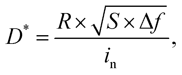
It is noteworthy that the photocurrent of the heterojunction device exhibits a linear correlation across four orders of magnitude of incident power intensity variation (with a confidence level of 99.6%) (Fig. 3b). Consequently, the 80.9 dB linear dynamic range (LDR) can serve as a reference for linear calibration across a wider range of light intensities. Responsivity (R) and specific detectivity (D*) are defined as follows:34–36
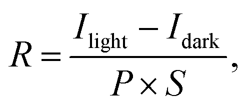
where S represents the effective area of the device, P is the incident light power intensity, in is the noise current, and Δf is the working bandwidth. The R is negatively correlated with the incident light intensity (Fig. 3c), indicating that the device has better extraction efficiency under weak light conditions. The heterostructure device achieves a maximum R of 11.2 A W−1 under 530 nm laser illumination at an intensity of 13 μW cm−2 and a bias of −5 V. The in is obtained from the noise power density spectrum (Fig. S5, ESI†), where the noise current exhibits pronounced thermal noise (1/f noise) characteristics.15,37 Therefore, to accurately describe the detection performance of the heterostructure device, it is necessary to specify its operating frequency. At an operating frequency of 1 Hz, the maximum D* of the device is 6.17 × 10¹⁰ Jones and it decreases linearly with increasing illumination power (Fig. 3c). Furthermore, the device exhibits optical switching behavior under periodic 530 nm irradiation (Fig. 3d). The response times are 16 ms for the rise time (τr) and 30 ms for the decay time (τd).
The heterogeneous integration of the device effectively extends the response wavelength of 2D BA2MA2Pb3I10 into the absorption region of GaAs. The wavelength-dependent response spectrum (Fig. 4a) covers a broad range from UV to NIR (300–840 nm). Interestingly, a narrowband response with a full width at half maximum (FWHM) of 22 nm appears at 630 nm. Compared to the absorption and PL spectrum of BA2MA2Pb3I10 sheets (Fig. S6, ESI†), the peak position of the narrowband response shows a redshift of approximately 13 nm. This sub-bandgap absorption beyond the band edge likely originates from the strong absorption of self-trapped states in the 2D RP perovskite and ionization by the electric field established in the GaAs/BA2MA2Pb3I10 depletion region.11,24 This indicates that our fabricated GaAs/BA2MA2Pb3I10 heterostructure photodetector can operate in photovoltaic mode. To understand the working mechanism, kelvin probe force microscopy (KPFM) was further employed to determine the surface potential difference of the heterostructure (Fig. 4b). The Fermi energy level of BA2MA2Pb3I10 is determined to be approximately 134 meV higher than that of GaAs. Accordingly, the energy band alignment is depicted in Fig. 4c, based on the known bandgap.38,39 The Fermi level difference causes the GaAs energy band to bend upwards and the BA2MA2Pb3I10 energy band to bend downwards, forming a spatial depletion region. Under illumination, photogenerated carriers in the depletion region are separated into GaAs and BA2MA2Pb3I10, respectively, creating an effective concentration gradient that generates a positive photovoltaic current in the external circuit.
 | ||
| Fig. 4 The energy band analysis of the GaAs/BA2MA2Pb3I10 heterostructure. (a) The responsivity of the device under different wavelengths at −5 V bias. The light intensity at different wavelengths was calibrated using standard Si devices. (b) KPFM topological images of the surface of the GaAs/BA2MA2Pb3I10 junction. (c) The energy band diagram of the carrier extraction process in the GaAs/BA2MA2Pb3I10 heterostructure under self-driven mode. | ||
To validate this, we investigate the performance of the heterostructure device operating in photovoltaic mode. Under 0 V bias, the currents of the device are tested under illumination of different wavelengths with the same intensity (Fig. 5a). The self-powered device achieves a maximum current of approximately 270 pA at 530 nm, which is predictable as both GaAs and BA2MA2Pb3I10 can generate photogenerated carriers under green light illumination. Additionally, the self-powered device combines the advantages of GaAs, allowing it to efficiently detect NIR light. Even without a bias, the response speed of the device remains in the millisecond range (Fig. 5b), with a τr of 66 ms and a τd of 72 ms under 530 nm illumination. This outperforms some 2D perovskite and GaAs devices operating under bias.24,40,41 The perovskite-based device maintains superior relative stability without bias. Remarkably, even for this low-dimensional heterogeneous integration device, a stable switching response is maintained after continuous testing in an air environment for 250 s (Fig. 5c).
 | ||
| Fig. 5 The self-driven photoresponse of the GaAs/BA2MA2Pb3I10 heterostructure photodetector. (a) The variation of device photocurrent with irradiation wavelength (consistent power intensity) in self-driven mode. Temporal photocurrent (b) and continuous photo and dark current (c) measurements during 0 V bias under 530 nm illumination at the intensity of 143.2 mW cm−2. | ||
Conclusions
In summary, we have demonstrated an effective approach for the non-exfoliated heterogeneous integration of 2D RP perovskites and successfully constructed a 1D GaAs nanowire/2D BA2MA2Pb3I10 sheet heterostructure. The large-area, high crystallinity, and flat surface phase-pure 2D RP perovskite sheets provide a foundation for their vdW integration. The favorable vdW contacts create a remarkably low dark current of 1.94 pA. Based on this, the excellent performance of the device is obtained, featuring an LDR of 80.9 dB, an R of 11.2 A W−1, a D* of 6.17 × 10¹⁰ Jones, and a photoresponse speed of 16 ms. The integration with GaAs nanowires broadens the response spectrum of 2D perovskite into the NIR range. Ultimately, the potential difference of 134 mV across the vdW heterostructure enables the device to operate self-driven for rapid, and stable operation across UV to NIR spectral ranges. This work informs perovskite heterostructure integration and provides a foundation for broader van der Waals heterostructure development.Experimental section
Synthesis of the perovskite precursors
The raw materials 38.2 mg butylammonium iodide (BAI, Xiàn Polymer Light Technology Co., Ltd, 99.0%), 63.6 mg methylamine iodide (MAI, Xiàn Polymer Light Technology Co., Ltd, 99.99%) and 272.0 mg lead iodide (PbI2, Xiàn Polymer Light Technology Co., Ltd, 99.99%) were dissolved in a solvent mixture of 940 μL hydroiodic acid (HI, Aladdin Chemistry Co., Ltd, 55.0–58.0% in H2O, contains 1.5% H3PO2 as a stabilizer,) and 60 μL hypophosphorous acid (H3PO2, Aladdin Chemistry Co., Ltd, 50% in H2O). The mixture was constantly stirred at 95 °C temperatures until the clear dark-red solution was obtained.Fabrication of the GaAs/BA2MA2Pb3I10 heterostructure photodetector
(i) Initially, GaAs nanowires were transferred from a silicon substrate to a Si/SiO2 substrate equipped with positional markers via a physical transfer method. To ensure robust adhesion to the substrate, the excess nanowires were subsequently rinsed with isopropyl alcohol. Uniform and planar photolithographic mask layers were achieved through spin-coating and annealing processes utilizing methyl methacrylate (MMA) and polymethyl methacrylate (PMMA) as electron beam photoresists. The GaAs nanowires were subsequently patterned at predetermined locations using an electron beam lithography system (JEOL JSM-IT300). Ultimately, Cr/Au (10/80 nm) patterned electrodes were fabricated via thermal vapor deposition. (ii) The perovskite precursor solution was held on a hot plate at 80 °C. A 10 μL drop of the heated precursor solution was then deposited onto a hydrophobic slide. Phase-pure 2D RP perovskite flakes rapidly crystallized at the air–solution interface as the solution cooled. These perovskite flakes were then simultaneously picked up in parallel using polydimethylsiloxane (PDMS, GelPak, PF-30-X4) stamps. Since PDMS is hydrophobic, little solvent remains on the stamp. The synthesis of 2D PR perovskite was carried out in air with a relative humidity of 72%. (iii) GaAs nanowires (i) and PDMS stamps with adsorbed perovskite flakes (ii) were vertically aligned on a transfer stage (Metatest, E1-T) under a microscope. The XYZ position of the perovskite sheets on the stamp was precisely adjusted to ensure contact both with the nanowire and with Au, respectively, and appropriate Z-direction pressure was applied. Strong vdW forces between the substrate and the perovskite sheet cause the latter to remain on the substrate when the stamp is lifted slowly.Characterization of the GaAs/BA2MA2Pb3I10 heterostructure
The optical images were obtained with a Zeiss AxioCam ICC 5 microscope. The surface morphologies of phase-pure 2D RP perovskite flakes and GaAs nanowires were obtained by scanning electron microscopy (SEM, Sigma FE-SEM, Zeiss, Germany). Energy-dispersive X-ray spectroscopy (EDS) mapping were acquired by the Zeiss FE-SEM instrument. The thicknesses and surface potential distribution data of the 2D perovskite and nanowires were characterized by AFM (FastScanBio-Icon, Bruker, US). The PL spectra were studied using a Confocal Laser Raman Spectrometer (LabRAM HR Evolution, HORIBA, Japan) with a 325 nm continuous laser. Absorption spectra were performed on a UV-Vis spectrophotometer (V770, JASCO, Japan).The optoelectronic characteristics (I–V, I–t) were measured on a semiconductor device analyzer (B1500A, Keysight, US) equipped with a probe station (Semishare, China) and a silver probe, and the excitation light source adopted commercial laser diodes with wavelengths of 530 nm and 650 nm. The laser intensity was regulated by a neutral density filter (FW2AND, Thorlabs) and the optical power density was measured by a power meter (PM100D, Thorlabs). The transient photoresponse was measured using a digital oscilloscope (MDO4054C, Tektronix, US) in conjunction with a low-noise current preamplifier (SR570, Stanford Research Systems, US), and the optical switch of the laser source was controlled with a function/arbitrary waveform generator (DG4602, RIGOL, China). The response spectrum and multi-wavelength spectrum were acquired using a photodetector spectral responsivity calibration system equipped with a monochromator (DSR600, Zolix Instruments, China), a lock-in amplifier (SR830, Stanford Research Systems, US), a mechanical chopper (SR540, Stanford, US), and a 150-W xenon lamp. Noise current was measured at different frequencies (from 0.01 Hz to 1000 Hz) by a lock-in amplifier (Stanford Research System, SR830), and the device was supplied with −5.0 V through the source meter (Agilent-Keysight B2902A). All the measurements were conducted under an ambient environment.
Author contributions
The manuscript was written through the contributions of all authors. All authors have approved the final version of the manuscript.Data availability
The data supporting this article have been included as part of the ESI.†Conflicts of interest
There are no conflicts to declare.Acknowledgements
This work was financially supported by the National Natural Science Foundation of China (12074045, 62027820, 61904017), the Natural Science Foundation of Jilin Province (No. 20230101352JC), and the “111” Project of China (D17017). W.-S.-P thanks the support from the Science and Technology Development Fund, Macao SAR (file no. 0083/2023/ITP) and the Multi-year Research Grants (MYRG-GRG2023-00230-IAPME-UMDF, MYRG-CRG2022-00016-ICMS) from the University of Macau.References
- J. Y. Kim, J.-W. Lee, H. S. Jung, H. Shin and N.-G. Park, Chem. Rev., 2020, 120, 7867–7918 CrossRef CAS PubMed.
- L. Zhang, L. Mei, K. Wang, Y. Lv, S. Zhang, Y. Lian, X. Liu, Z. Ma, G. Xiao and Q. Liu, Nano-Micro Lett., 2023, 15, 177 CrossRef PubMed.
- T.-H. Han, K. Y. Jang, Y. Dong, R. H. Friend, E. H. Sargent and T.-W. Lee, Nat. Rev. Mater., 2022, 7, 757–777 CrossRef.
- T. Wu, Z. Qin, Y. Wang, Y. Wu, W. Chen, S. Zhang, M. Cai, S. Dai, J. Zhang and J. Liu, Nano-Micro Lett., 2021, 13, 1–18 CrossRef.
- A. S. Bati, Y. L. Zhong, P. L. Burn, M. K. Nazeeruddin, P. E. Shaw and M. Batmunkh, Commun. Mater., 2023, 4, 2 CrossRef CAS.
- Y. Zhao, X. Yin, P. Li, Z. Ren, Z. Gu, Y. Zhang and Y. Song, Nano-Micro Lett., 2023, 15, 187 CrossRef CAS.
- J. Xiong, Z.-H. Zhang, Z. Li, P. Zheng, J. Li, X. Zhang, Z. Gao, Z. Wei, G. Zheng and S.-P. Wang, Light: Sci. Appl., 2023, 12, 286 CrossRef CAS PubMed.
- A. Fakharuddin, M. K. Gangishetty, M. Abdi-Jalebi, S.-H. Chin, A. R. bin Mohd Yusoff, D. N. Congreve, W. Tress, F. Deschler, M. Vasilopoulou and H. J. Bolink, Nat. Electron., 2022, 5, 203–216 CrossRef CAS.
- Y.-K. Wang, F. Jia, X. Li, S. Teale, P. Xia, Y. Liu, P. T.-S. Chan, H. Wan, Y. Hassan and M. Imran, Sci. Adv., 2023, 9, eadh2140 CrossRef CAS PubMed.
- Y. W. Hsiao, B. S. Cheng, H. C. Hsu, S. H. Wu, H. T. Wu, C. C. Leu and C. F. Shih, Adv. Funct. Mater., 2023, 33, 2300169 CrossRef CAS.
- J. Wang, J. Li, S. Lan, C. Fang, H. Shen, Q. Xiong and D. Li, ACS Nano, 2019, 13, 5473–5484 CrossRef CAS.
- S. Liu, Y. Chen, W. Gao, W. Li, X. Yang, Z. Li, Z. Xiao, Y. Liu and Y. Wang, Adv. Mater., 2023, 35, 2303544 CrossRef CAS.
- Y. Zhang, C. Wu, X. Zhou, J. Li, X. Tao, B. Liu, J. Chen, Y. Chang, G. Tong and Y. Jiang, Mater. Today Phys., 2023, 36, 101179 CrossRef CAS.
- L. Chao, T. Niu, W. Gao, C. Ran, L. Song, Y. Chen and W. Huang, Adv. Mater., 2021, 33, 2005410 CrossRef CAS.
- L. Wang, X. Zou, J. Lin, J. Jiang, Y. Liu, X. Liu, X. Zhao, Y. F. Liu, J. C. Ho and L. Liao, ACS Nano, 2019, 13, 4804–4813 CrossRef CAS.
- A. K. Geim and I. V. Grigorieva, Nature, 2013, 499, 419–425 CrossRef CAS.
- A. Castellanos-Gomez, X. Duan, Z. Fei, H. R. Gutierrez, Y. Huang, X. Huang, J. Quereda, Q. Qian, E. Sutter and P. Sutter, Nat. Rev. Methods Primers, 2022, 2, 58 CrossRef CAS.
- D. Jariwala, T. J. Marks and M. C. Hersam, Nat. Mater., 2017, 16, 170–181 CrossRef CAS PubMed.
- P. Wang, C. Jia, Y. Huang and X. Duan, Matter, 2021, 4, 552–581 CrossRef CAS.
- D. Liu, Y. Zheng, X. Y. Sui, X. F. Wu, C. Zou, Y. Peng, X. Liu, M. Lin, Z. Wei and H. Zhou, Nat. Commun., 2024, 15, 2390 CrossRef CAS PubMed.
- S.-S. Yan, Y.-C. Kong, Z.-H. Zhang, Z.-S. Wu, Z.-D. Lian, Y.-P. Zhao, S.-C. Su, L. Li, S.-P. Wang and K. W. Ng, ACS Appl. Mater. Interfaces, 2022, 14, 49975–49985 CrossRef CAS.
- C. R. Roy, D. Pan, Y. Wang, M. P. Hautzinger, Y. Zhao, J. C. Wright, Z. Zhu and S. Jin, J. Am. Chem. Soc., 2021, 143, 5212–5221 CrossRef CAS.
- Z. Gu, Z. Huang, C. Li, M. Li and Y. Song, Sci. Adv., 2018, 4, eaat2390 CrossRef PubMed.
- J. Li, J. Wang, J. Ma, H. Shen, L. Li, X. Duan and D. Li, Nat. Commun., 2019, 10, 806 CrossRef PubMed.
- Y. Chen, Y. Sun, J. Peng, J. Tang, K. Zheng and Z. Liang, Adv. Mater., 2018, 30, 1703487 CrossRef.
- L. Zhao, H. Tian, S. H. Silver, A. Kahn, T.-L. Ren and B. P. Rand, Joule, 2018, 2, 2133–2144 CrossRef CAS.
- Q. Fu, X. Wang, F. Liu, Y. Dong, Z. Liu, S. Zheng, A. Chaturvedi, J. Zhou, P. Hu and Z. Zhu, Small, 2019, 15, 1902890 CrossRef PubMed.
- W. Su, S. Zhang, C. Liu, Q. Tian, X. Liu, K. Li, Y. Lv, L. Liao and X. Zou, Nano Lett., 2022, 22, 10192–10199 CrossRef CAS.
- J. Guo, B. Ye, Y. Gu, Y. Liu, X. Yang, F. Xie, X. Zhang, W. Qian, X. Zhang and N. Lu, ACS Appl. Mater. Interfaces, 2023, 15, 56014–56021 CrossRef CAS PubMed.
- D. Pan, Y. Fu, N. Spitha, Y. Zhao, C. R. Roy, D. J. Morrow, D. D. Kohler, J. C. Wright and S. Jin, Nat. Nanotechnol., 2021, 16, 159–165 CrossRef CAS.
- Z. Li, Y. Lin, H. Gu, N. Zhang, B. Wang, H. Cai, J. Liao, D. Yu, Y. Chen and G. Fang, Sci. Bull., 2024, 69, 382–418 CrossRef CAS.
- Y. Kang, G. Na, D. Wang, J. Tang, L. Zhang, Y. Shan, C. Cong, Z. Wei and R. Chen, ACS Photonics, 2021, 8, 2889–2897 CrossRef CAS.
- X. Li, X. Yu, H. Zeng, G. Boras, K. Shen, Y. Zhang, J. Wu, K. L. Choy and H. Liu, Appl. Phys. Lett., 2021, 119, 053105 CrossRef CAS.
- Z. Zhang, P. Zheng, S. S. Yan, B. S. Qiao, K. W. Ng, H. C. Liu, S. P. Wang and Z. Wei, Adv. Opt. Mater., 2023, 11, 2201847 CrossRef CAS.
- Z.-H. Zhang, S.-S. Yan, Y.-L. Chen, Z.-D. Lian, A. Fu, Y.-C. Kong, L. Li, S.-C. Su, K.-W. Ng and Z.-P. Wei, ACS Appl. Mater. Interfaces, 2024, 16, 10398–10406 CrossRef CAS.
- Q. Tian, R. Hong, C. Liu, X. Hong, S. Zhang, L. Wang, Y. Lv, X. Liu, X. Zou and L. Liao, Nano Lett., 2021, 22, 494–500 CrossRef PubMed.
- F. Wang, X. Zou, M. Xu, H. Wang, H. Wang, H. Guo, J. Guo, P. Wang, M. Peng and Z. Wang, Adv. Sci., 2021, 8, 2100569 CrossRef CAS.
- X. Hou, X. Hong, F. Lin, J. Cui, Q. Dai, Q. Tian, B. Meng, Y. Liu, J. Tang and K. Li, Photonics Res., 2023, 11, 541–548 CrossRef CAS.
- T. Yan, F. Liu, Y. Wang, J. Yang, C. Ding, Y. Cai, Z. Wu, X. Zhan, F. Wang and Y. Tian, Adv. Electron. Mater., 2022, 8, 2101385 CrossRef CAS.
- X. Zhu, F. Lin, Z. Zhang, X. Chen, H. Huang, D. Wang, J. Tang, X. Fang, D. Fang and J. C. Ho, Nano Lett., 2020, 20, 2654–2659 CrossRef CAS PubMed.
- S. Liu, W. Gao, Y. Chen, X. Yang, K. Niu, S. Li, Y. Xiao, Y. Liu, J. Zhong and J. Xia, Nano Lett., 2024, 24, 7724–7731 CrossRef CAS PubMed.
Footnote |
| † Electronic supplementary information (ESI) available: Experimental details include the statistics of BA2MA2Pb3I10 sheet thickness; EDS element mapping images of the heterostructure device, the optical microscope image of the GaAs/BA2MA2Pb3I10 heterostructure photodetector, the I–V curves of GaAs and BA2MA2Pb3I10 devices, and comparison of the device normalized photocurrent with the BA2MA2Pb3I10 PL and absorption spectrum. See DOI: https://doi.org/10.1039/d4tc02994a |
| This journal is © The Royal Society of Chemistry 2024 |