
 Open Access Article
 This Open Access Article is licensed under a
 Creative Commons Attribution 3.0 Unported Licence
Electrodeposition of 2D layered tungsten diselenide thin films using a single source precursor†
Shibin
Thomas
 *a,
Victoria K.
Greenacre
a,
Jiapei
Zhang
b,
Nikolay
Zhelev
a,
Sami
Ramadan
c,
Yisong
Han
d,
Richard
Beanland
d,
Nema M.
Abdelazim
b,
Yasir J.
Noori
b,
Kees
de Groot
b,
Gillian
Reid
*a and
Philip N
Bartlett
*a
*a,
Victoria K.
Greenacre
a,
Jiapei
Zhang
b,
Nikolay
Zhelev
a,
Sami
Ramadan
c,
Yisong
Han
d,
Richard
Beanland
d,
Nema M.
Abdelazim
b,
Yasir J.
Noori
b,
Kees
de Groot
b,
Gillian
Reid
*a and
Philip N
Bartlett
*a
aSchool of Chemistry and Chemical Engineering, University of Southampton, Southampton, SO17 1BJ, UK. E-mail: shibin.thomas@soton.ac.uk; G.Reid@soton.ac.uk; P.N.Bartlett@soton.ac.uk
bSchool of Electronics and Computer Science, University of Southampton, Southampton, SO17 1BJ, UK
cDepartment of Materials, Imperial College, London, SW7 2AZ, UK
dDepartment of Physics, University of Warwick, Coventry, CV4 7AL, UK
First published on 15th October 2024
Abstract
The development of area-selective, scalable deposition methods for the anisotropic growth of transition metal dichalcogenide (TMDC) thin films with a planar morphology is essential for their practical applications in integrated electronic and optoelectronic devices. In this work, we report on the electrodeposition of layered WSe2 from a single source molecular precursor, containing both W and Se, for the first time. Using WSeCl4 in an acetonitrile (MeCN) electrolyte solution, we have employed cyclic voltammetry (CV) and electrochemical quartz crystal microbalance (EQCM) techniques to study the electrochemical behaviour of WSeCl4. A pulsed electrodeposition technique was then used to deposit WSe2 films, which possess a homogeneous composition across the whole electrode area. Characterization using scanning and transmission electron microscopy, X-ray diffraction, X-ray photoelectron spectroscopy and Raman spectroscopy confirm the electrodeposited thin films to be WSe2. As a proof-of-concept for future growth directly into 3D device architectures, we present the 2D anisotropic growth of WSe2 thin films from the edge of a 100 nm thick TiN nanoband electrode across SiO2 on microfabricated 3D structures, allowing the direct measurement of electrical characteristics. Through this work, we also demonstrate electrodeposition as an area-selective growth technique suitable for obtaining highly anisotropic WSe2 thin films which are very promising for future electronic and optoelectronic applications.
Introduction
Transition metal dichalcogenides (TMDCs) form a very interesting family of 2D materials with unique electronic and optical properties, making them attractive candidates for applications in modern electronic and optoelectronic devices.1,2 Structurally, they are layered hexagonal materials, somewhat analogous to graphene, with strong covalent in-layer bonding and with the adjacent layers held together via weak van der Waals interactions. Importantly, unlike graphene, TMDCs have a band gap, and are therefore semiconducting. The size of the band gap is also tuneable. Hence, mono- and few-layer TMDCs exhibit distinctly different properties from their bulk counterparts.3,4Among the various semiconducting TMDC materials, WSe2 stands out as a p-type material, in contrast to most of the other TMDCs, which are usually n-type.5,6 This makes WSe2 an attractive candidate for fabricating TMDC heterostructure devices, such as p–n junctions7,8 or ambipolar transistors.9,10 Field effect transistor devices based on WSe2 have already been demonstrated.11,12 However, to-date, the majority of studies on WSe2 semiconductors have used mechanically exfoliated samples, and while this work has demonstrated some of the potential for novel devices, exfoliation is unsuitable for mass-production since it is time-consuming and offers limited control over the size and thickness (number of layers).13 Large scale applications and device fabrication with WSe2 require developing controllable and scalable deposition methods that are capable of delivering highly ordered (crystalline) 2D layers, and ideally without the need for post-deposition transfer and/or patterning of the material. The importance of developing controlled patterning of TMDCs with programable geometries has been discussed in a recent review.14 A number of other physical15–17 and chemical techniques,18–21 including chemical vapour deposition (CVD),22,23 have been developed to deposit WSe2 films. These are scalable and versatile techniques, enabling the production of ultra-thin TMDCs at full wafer scale with high crystal quality and excellent electronic properties. On the other hand, these techniques offer little scope for direct area-selective growth, hence they usually require film transfer and post-deposition patterning and etching. They also usually involve conditions such as high temperature and/or ultra-high vacuum.
Electrodeposition has recently emerged as a potential low-cost alternative technique for the deposition of functional metal chalcogenide materials for semiconducting24,25 and catalytic26,27 applications. Electrodeposition occurs via ‘unit-by-unit’ growth (or atom-by-atom growth for single element films) from the electrode surface, and therefore, it is possible to tune the deposit morphology and thickness by controlling the electrochemical parameters, such as the applied potential, current or deposition time. Moreover, the material growth starts from the areas defined by the electrical contact and the dimensions of the electrode, making it possible to deposit materials over complex nanoscale features and topologically-demanding surfaces. It is a technique typically performed in ambient conditions and benefits from scalability that suits industrial mass-scale device fabrication processes (e.g. Cu on–chip interconnections).28
There are several reports in the literature on the electrodeposition of TMDCs from acidic aqueous electrolytes, primarily focusing on MoS2, mostly for catalytic applications where the presence of rough and irregular materials is advantageous.27,29 However, obtaining ordered 2D layered TMDCs, especially tungsten-based TMDCs, via electrodeposition remains highly challenging due to: (i) the lack of readily available electroactive precursors able to deliver both the metal and the chalcogen in the electrolyte to allow electrodeposition of the target material; (ii) the limited range of solvents that are both compatible with the precursors and also have a sufficiently wide electrochemical window to achieve the required deposition; (iii) the difficulties in tuning and optimising the electrochemical parameters to obtain stoichiometric, high quality layered TMDCs, and (iv) being compound semiconductor materials, the greater complexity of the one-step electrodeposition process for TMDCs compared to single element electrodepositions.
In an effort to address these challenges, we have recently developed tailor-made single source precursors (SSPs) for non-aqueous electrodeposition of MoS2 and WS2, demonstrating (after annealing) the growth of mono- and few-layer 2D films.30–32 Electrochemical growth of a 2D heterostructure was also demonstrated by depositing WS2 monolayers onto graphene.33
The electrical characterization of TMDCs usually requires materials deposited on an insulating substrate, however, electrodeposition typically produces thin films on top of a conducting substrate, which then dominates electrical measurements. To address this challenge, we have demonstrated the growth of MoS2 thin films over an insulating surface (SiO2) by implementing fabricated nanoband electrodes.34 Using this approach, the MoS2 nucleation occurs at the narrow (10s of nm) electrode edges and, together with the intrinsic 2D anisotropy of the MoS2, promotes the growth away from the electrode and out over the insulator. As well as driving the 2D growth, this approach also facilitates electrical characterization of the electrodeposited films directly, without needing a material transfer step.
With regard to prior work on the electrodeposition of WSe2, there is some literature that discusses ‘conventional’ aqueous electrodeposition using dual source precursors (e.g. using H2WO4 and SeO2),35–37 however, no developments on the applications of these electrodeposited materials have been reported. Electrodeposition using dual source precursors usually involves complex multi-step reduction processes, and the large difference in the reduction potentials of W and Se presents a further barrier to effective and controlled deposition. None of the reported works present evidence, e.g. via electron microscopy or Raman spectroscopy, for the WSe2 being in the form of 2D layers. Additionally, the use of aqueous electrolytes has limitations due to the narrow electrochemical window and possible H2 evolution reaction occurring alongside deposition of the target material.
Our hypothesis to achieve improved control of the electrochemical growth of ultrathin WSe2 2D layers requires the development of a SSP, i.e., a compound incorporating both W and Se, directly bonded, in a single molecular entity. This also needs to be compatible with non-aqueous electrolyte media and enable easy removal of ligands and by-products. In previous work we have reported the CVD growth of WSe2 and WS2 thin films from the SSPs, [WSeCl4(SenBu2)] and [WSCl4(SnBu2)], respectively, derived from coordination of the chalcogenoether to WSeCl422 or WSCl4.38 We subsequently identified the salt, [NEt4]2[WS2Cl4], as a suitable SSP for electrodeposition of WS2.32 For tungsten diselenide electrodeposition, therefore, we considered the analogous salt, [NEt4]2[WSe2Cl4], as a potential SSP candidate. However, we were unable to isolate it.22 Therefore, we turned to WSeCl4 itself as a possible SSP. In this article we demonstrate the suitability of WSeCl4 for the electrodeposition of layered WSe2 thin films from acetonitrile (MeCN).
Initially, investigations of the electrochemical behaviour of WSeCl4 using cyclic voltammetry (CV) and electrochemical quartz crystal microbalance (EQCM) techniques are discussed and the resulting electrodeposited WSe2 films are characterised using various microscopic and spectroscopic techniques. The growth of WSe2 films out from the edge of micro-structured TiN nanoband electrodes, over SiO2, is then demonstrated for the first time, together with their electrical characteristics. This work provides a very promising proof-of-concept for further development towards potential future electronic device applications.
Experimental
WSeCl4 was synthesised by heating WCl6 and Sb2Se3in vacuo, as detailed in our recent work.22,39 All the electrolyte preparations, electrochemical characterization and electrodeposition experiments were performed inside an N2 filled recirculating glove box (Belle Technology, UK) with sub-10 ppm O2 and H2O levels. Electrolyte solutions were prepared in anhydrous MeCN (Fisher, 99.9%), further dried and degassed by refluxing with CaH2, followed by distillation under N2. 0.1 M [Et4N]Cl (Sigma-Aldrich, ≥99.0%, dried in vacuo) was used as the supporting electrolyte. CV and electrodeposition experiments used a three-electrode system with an Autolab potentiostat (μAUT70706). A Pt mesh was used as the counter electrode and the reference electrode was Ag/AgCl (in 0.1 M [Et4N]Cl in MeCN). All the applied potentials reported were recorded against Ag/AgCl. The Pt mesh counter electrode was cleaned by rinsing with de-ionised water and heating in a butane/propane flame (70% butane, 30% propane). A circular (0.4 cm diameter) titanium nitride (TiN) substrate (200 nm coating of TiN on Si) was employed as the working electrode for the initial electrodeposition work. The sheet resistance of the TiN was measured as 8.20 Ω sq−1, hence the voltage drop is negligible. The EQCM (QCM 200, SRS) system used a Pt-coated 5 MHz AT-cut quartz crystal (1.3 cm diameter). The microfabrication technique for the preparation of the TiN nanoband electrodes was as we have described previously.34 After the electrodeposition, the substrates were rinsed with fresh MeCN solvent, followed by isopropyl alcohol. Samples for annealing were dried under reduced pressure (0.1 mbar) at 120 °C for 10 min and then annealed at 700 °C for 10 min in a tube furnace under reduced pressure (0.1 mbar).A field emission scanning electron microscope (FE-SEM, ZEISS Sigma 500 VP), coupled with an Oxford Instruments Ultim Max 170 mm2 energy dispersive X-ray spectroscopy (EDS) detector, and an additional WITec correlative Raman microscope (RISE), was used to determine the film morphology, composition and Raman features of samples all at the same position. Typically, accelerating voltages of 5 kV or less were used to maximise the contrast and signal from the film's surface. The calibration of the EDS quantification was confirmed by comparison to a standard WSe2 single crystal sample (Ossila Technologies). Raman spectra were obtained with 532 nm laser excitation at 1 mW power. X-ray diffraction (XRD) patterns were collected in grazing incidence mode (ω1 = 1°) using a Rigaku SmartLab diffractometer (Cu-Kα, λ = 1.5418 Å) with parallel X-ray beam and a Hypix detector used in 1D mode. A JEOL ARM200F operated at 200 kV was used to collect scanning transmission electron microscopy (STEM) images. X-ray photoelectron spectroscopy (XPS) was performed with Kα+ and an Al radiation source (hν = 1486.6 eV) in an ultrahigh vacuum chamber with a base pressure of 5 × 10⁻⁸ mbar. Optical microscopic images were recorded with a Nikon LV100ND light microscope.
Results and discussion
Evaluation of WSeCl4 as a SSP for electrodeposition of WSe2
The electrochemical behaviour of WSeCl4 was initially studied by conducting CV measurements on a TiN electrode. Fig. 1a shows the CV from a 5 mM solution of WSeCl4 in MeCN with 0.1 M [Et4N]Cl supporting electrolyte. In comparison to the CV of the background electrolyte (Fig. S1, ESI†), upon scanning to negative potential an increase in reduction current originating from −0.65 V is visible in the CV, which progresses to produce a peak shoulder at −1.05 V and thereafter two reduction peaks at −1.40 V and −1.71 V. These large reduction waves correspond to the electroreduction of WSeCl4 as demonstrated by further experiments discussed below. In the reverse scan, there is no anodic oxidation or stripping peak until +1.35 V, indicating the irreversible nature of the reduction products at the electrode. The increase in current after +1.35 V corresponds to the anodic decomposition of the electrolyte. Multiple CV scans performed on TiN electrode (Fig. S2, ESI†) also show similar electrochemical features as observed in the CV in Fig. 1a. However, after the first cycle, the onset of the reduction current shifts slightly to more positive potentials. This shift is expected because the TiN electrode is covered with a film deposited from the first cycle and therefore the active electrode is no longer TiN. Additionally, the two distinct reduction peaks (−1.40 V and −1.71 V) observed in the first cycle become less resolved, appearing as a single broad peak, noticeable from cycle 3. | ||
| Fig. 1 (a) Cyclic voltammogram of 5 mM WSeCl4 in MeCN on a TiN electrode. The supporting electrolyte is 0.1 M [Et4N]Cl and the scan rate is 50 mV s−1. Arrows indicate the direction of potential scanning; the starting potential is 0 V. (b) Schematic illustration of the electrodeposition of WSe2 onto a TiN electrode. | ||
Clearly the WSeCl4 precursor (W![[thin space (1/6-em)]](https://www.rsc.org/images/entities/char_2009.gif) :Se ratio = 1) does not have the ideal ratio to form WSe2, requiring further selenium, e.g. from Se atom transfer from a second WSeCl4 molecule, to give the necessary 1:2 ratio. Hence, it is likely that at least one other tungsten species is also formed during the process. The exact speciation in the electrolyte solution when WSeCl4 is dissolved is not easily determined. However, comparison can be made to the sulfur analogue, WSCl4, which reacts with (Me3Si)2S (a source of S2−) and Et4NCl to form [NEt4]2[WS2Cl4], which is a SSP for WS2 electrodeposition.32 As discussed, while the corresponding [NEt4]2[WSe2Cl4] salt could not be isolated, it is possible that this exists in the electrolyte solution in situ.22 Moreover, the coordination chemistry of WSeCl422 can be compared to that of WSCl4.40,41 This clearly shows that the W
:Se ratio = 1) does not have the ideal ratio to form WSe2, requiring further selenium, e.g. from Se atom transfer from a second WSeCl4 molecule, to give the necessary 1:2 ratio. Hence, it is likely that at least one other tungsten species is also formed during the process. The exact speciation in the electrolyte solution when WSeCl4 is dissolved is not easily determined. However, comparison can be made to the sulfur analogue, WSCl4, which reacts with (Me3Si)2S (a source of S2−) and Et4NCl to form [NEt4]2[WS2Cl4], which is a SSP for WS2 electrodeposition.32 As discussed, while the corresponding [NEt4]2[WSe2Cl4] salt could not be isolated, it is possible that this exists in the electrolyte solution in situ.22 Moreover, the coordination chemistry of WSeCl422 can be compared to that of WSCl4.40,41 This clearly shows that the W![[double bond, length as m-dash]](https://www.rsc.org/images/entities/char_e001.gif) Se bond is weaker than WS in the W(VI) homologues. WSCl4 typically forms a chloride-bridged dimer42 or tetramer,43 whereas WSeCl4 is a monomeric square-based pyramid (from single crystal and powder X-ray diffraction data and gas phase density functional theory calculations). It has also been shown that WSeCl4 forms an MeCN adduct, [WSeCl4(NCMe)], and is susceptible to Se atom transfer, as evidenced by its reaction with phosphines to form phosphine selenides.22 The ease of abstraction of the selenium from WSeCl4, and the presence of chloride in the electrolyte solution could result in formation of a tungsten chloride species, such as WCl6, in the electrolyte. Based on this information, a plausible overall electrochemical reaction is shown in eqn (1).
Se bond is weaker than WS in the W(VI) homologues. WSCl4 typically forms a chloride-bridged dimer42 or tetramer,43 whereas WSeCl4 is a monomeric square-based pyramid (from single crystal and powder X-ray diffraction data and gas phase density functional theory calculations). It has also been shown that WSeCl4 forms an MeCN adduct, [WSeCl4(NCMe)], and is susceptible to Se atom transfer, as evidenced by its reaction with phosphines to form phosphine selenides.22 The ease of abstraction of the selenium from WSeCl4, and the presence of chloride in the electrolyte solution could result in formation of a tungsten chloride species, such as WCl6, in the electrolyte. Based on this information, a plausible overall electrochemical reaction is shown in eqn (1).
| 2WSeCl4 + 2e− → WSe2 + WCl6 + 2Cl− | (1) |
WCl6 is soluble in MeCN, forming an adduct, and extremely moisture sensitive, reacting rapidly with trace water. It is also known to be electrochemically active within the potential range where the WSe2 is deposited.44 We also confirmed this by performing a CV of WCl6 in MeCN, as shown in Fig. S3 (ESI†). Therefore, the reduction currents obtained in the CV (Fig. 1a) could have a contribution from the redox processes from the WCl6 liberated in the electrolyte during the electroreduction of WSeCl4.
To confirm the electroreduction of WSeCl4, potentiostatic depositions were performed by multiple experiments holding the applied potential at −1.3 V, −1.5 V and −1.8 V, respectively. In each case, a bluish-brown coloured thin film was obtained on the working electrode (Fig. S4, ESI†), confirming the formation of a deposit by cathodic electrodeposition. A schematic illustration of electrodeposition of WSe2 films on the TiN electrode is shown in Fig. 1b.
Further investigation of the CV was then undertaken to gain a more thorough understanding of the electrochemical processes at the interface to help in identifying the most appropriate applied potential for deposition and to control the growth rate and quality of the resulting films. EQCM is a highly sensitive technique to follow micro-scale mass changes occurring at the electrode surface during various electrochemical processes. It is particularly useful in combination with voltammetry to observe real-time mass changes during the potential scanning. The estimation of mass in EQCM experiments, assuming deposition of a rigid thin film, is based on the Sauerbrey equation.45
 | (2) |
Fig. 2(a) shows the CV of 5 mM WSeCl4 in MeCN recorded on a Pt-coated quartz crystal. The cathodic peaks in this CV appear slightly different from those in the CV on the TiN electrode (Fig. 1a). In this case three distinct reduction waves are observed in the cathodic scan, two smaller ones at −0.4 V and −0.75 V and a broad peak centred at −1.25 V. The broad reduction peak starting at −0.9 V matches well with the reduction peaks observed in the CV recorded on the TiN electrode discussed above, even though it appears as a single broad peak on Pt, in contrast to the two distinct peaks on TiN. This difference might be due to the distortions caused by the large surface area of the Pt quartz electrode and/or the differences in the electrochemistry on a polished Pt surface compared to that on TiN. Fig. 2(b) shows the corresponding mass changes during the CV scans. It is evident from the plot that the first two small cathodic peaks in the CVs do not contribute to any mass gain on the working electrode. However, corresponding to the broad cathodic peak starting from −0.9 V, there is an increase in mass, which continues on the return scan until the potential sweep reaches −0.9 V. This trend is observed in both CV cycles, and indicates electrodeposition processes in the potential window from −0.9 V to −2.0 V. This increase in mass is associated with the reduction of WSeCl4 to produce a WSe2 deposit, which, as we discuss later, is confirmed by potentiostatic deposition of thin films.
 | ||
| Fig. 2 (a) Two cycles of the CV from 5 mM WSeCl4 in MeCN on a Pt-coated quartz electrode. (b) The corresponding mass changes during the CV cycles. (c) Current transients during a potentiostatic deposition at −1.4 V for 5 min on a Pt-coated quartz electrode in EQCM and (d) the corresponding mass change during the potentiostatic deposition. The supporting electrolyte is 0.1 M [Et4N]Cl and the scan rate is 50 mV s−1. Arrows indicate the direction of potential scanning; the starting potential is 0 V. | ||
The EQCM measurements also help to identify the potential range and the optimum applied potential at which the deposition should be carried out to obtain the films. Note that the cathodic breakdown of the solvent/supporting electrolyte occurs beyond −1.8 V, hence less negative potentials are used to avoid contamination. Based on the EQCM data, −1.4 V was chosen for potentiostatic deposition and the current transient from a deposition performed on a Pt quartz crystal at −1.4 V for 5 min is shown in Fig. 2(c). Fig. 2(d) shows the corresponding mass changes during the potentiostatic deposition. There is a rapid rise in mass because of the nucleation, followed by a linear increase in mass with time, indicating smooth deposition of WSe2 onto the working electrode. This potentiostatic deposition performed on the EQCM electrode confirms that the applied potential of −1.4 V is suitable for growing thicker WSe2 films on the electrode. The mass calculated from the EQCM measurements is found to be small compared to the theoretical mass estimated from the charge passed, assuming a 2-electron reduction with 100% faradaic efficiency to deposit WSe2. The estimated current efficiency is ∼9%, consistent with the occurrence of side reactions, such as redox processes involving WCl6, or the formation of other soluble products during the deposition.
To further characterise the deposits, a thicker WSe2 film was obtained on a TiN electrode by potentiostatic electrodeposition in pulsing mode. While ultra-thin WSe2 films (sub-5 nm) are of most interest for the majority of applications, a 30 min deposition was performed to obtain sufficiently thick films to allow reliable characterization (e.g., by X-ray diffraction) to confirm the identity of the deposited material. Deposition in pulsing mode was employed because it can lead to smoother films compared to those obtained with normal potentiostatic deposition. Pulsed electrodeposition was carried out by holding the applied potential at −1.4 V for 5 s, followed by 0 V for 3 s, and 360 cycles were performed so that the total time held at −1.4 V was 30 min. Fig. 3(a) shows a top-view SEM image of the deposited film. The image shows a smooth and continuously grown layered thin film homogeneously covering the working electrode. Several cracks are evident from the SEM image, which are likely to be due to the lattice mismatch with TiN and the internal stresses during the relatively thick film growth. In contrast, using fewer pulses (60 cycles) leads to thinner films that are crack-free, as shown in Fig. 3(b). It is interesting to note here that the electrodeposition leads to large area (across the 0.4 cm diameter electrode) flat sheets of thin film by a laminar growth mechanism very typical for the 2D TMDCs. No significant solvent residues or particulates are observed on the deposited thin film, consistent with homogeneous growth and low surface roughness. The root mean square (RMS) roughness of the deposit, estimated from AFM measurements (Fig. S5, ESI†), is 11.9 nm. The AFM image also reveals large number of grains, indicative of the polycrystalline nature of the WSe2 film, as expected. The inset of Fig. 3a shows an EDS spectrum recorded from the deposited film. The EDS profile displays strong signals at 1.8 keV and 1.4 keV corresponding to the W (Mα) and Se (Lα) peaks, respectively. The atomic ratio of W to Se calculated from the EDS spectrum is 1:1.9. The N signal is from the underlying TiN electrode, and the small oxygen signal is most likely to be due to the surface oxidation of the film during handling outside the glove box (in air). The C signal originates from the adventitious carbon on the sample, as is commonly observed.
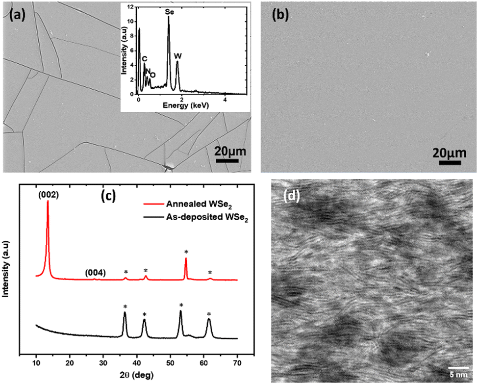 | ||
| Fig. 3 (a) Top-view SEM image of the deposit obtained after pulsed electrodeposition for 30 min from MeCN containing 5 mM WSeCl4 with 0.1 M [Et4N]Cl supporting electrolyte. The inset shows EDS profile of the deposited film. (b) Top-view SEM image of the deposit obtained after pulsed electrodeposition for 5 min. (c) Grazing incidence XRD pattern from the as-deposited and annealed WSe2 thin film. * Indicates substrate TiN/Si. (d) Cross-sectional annular dark-field STEM image of a WSe2 thin film after annealing. | ||
The as-deposited WSe2 film was found to be amorphous by X-ray diffraction (Fig. 3c). However, STEM analysis of this as-deposited thin film shows evidence for nanocrystalline WSe2 in the material. Fig. S6 (ESI†) shows the presence of nanoscale (5–10 nm) layered WSe2 in the as-deposited thin film, indicating some short to medium range order with small grain sizes.
In order to increase the grain size and to fully crystallise the thin film, thermal annealing was carried out in a tube furnace at 700 °C under vacuum for 10 min. This causes the film to become more crystalline, as evidenced by the XRD pattern (Fig. 3c), which shows a very intense peak at 2θ = 13.6°, corresponding to the (002) diffraction plane of WSe2,46 which dominates the diffraction pattern, along with the less intense (004) peak, showing significant preferred orientation in the 〈00l〉 direction. This is consistent with polycrystalline 4H WSe2 in space group P63/mmc. Lattice parameters were refined as: a = 3.358(17), c = 13.13(7) (Rwp = 8.79%; literature: a = 3.285(1); c = 12.961(1) Å).47 The other peaks in the XRD pattern correspond to the TiN/Si substrate.
Fig. 3d shows the cross-sectional STEM image of the WSe2 film after annealing, which confirms a significant increase in the grain size to ∼30 nm after ‘flash’ annealing, forming a stacked WSe2 multi-layer. These stacked layers are present even in the darker regions in the STEM image, which are found to be slightly W deficient.
The film composition was further investigated by XPS. Fig. 4a and b represent the elemental scans of W 4f and Se 3d orbitals, respectively. The featured peaks in Fig. 4a at 32.1 and 34.3 eV are attributed to the W 4f7/2 and W 4f5/2 components of WSe2, respectively. The positions of these peaks confirm the W to be in the +4 oxidation state, and are identical to WSe2 prepared by other methods.48,49 The additional weak peaks located at 35.5 and 37.6 eV are assigned as W 4f7/2 and W 4f5/2 from WO3, again likely to be due to the surface oxidation during the handling of the thin film in ambient atmosphere.50,51 This is also in agreement with the presence of a small oxygen signal in the EDS spectrum (Fig. 3a inset). As shown in Fig. 4b, the Se peak can be deconvoluted to the 54.3 and 55.2 eV peaks, corresponding to the doublet of Se 3d5/2 and 3d3/2, respectively.52 As dictated by the degeneracy, the ratios between the fitted peaks for the tungsten and sulfur peaks are fixed at 3:4 and 3:2, respectively. The XPS analysis further confirms that the electrodeposited film is WSe2, where a W to Se ratio of 1:2 is derived from the measurements.
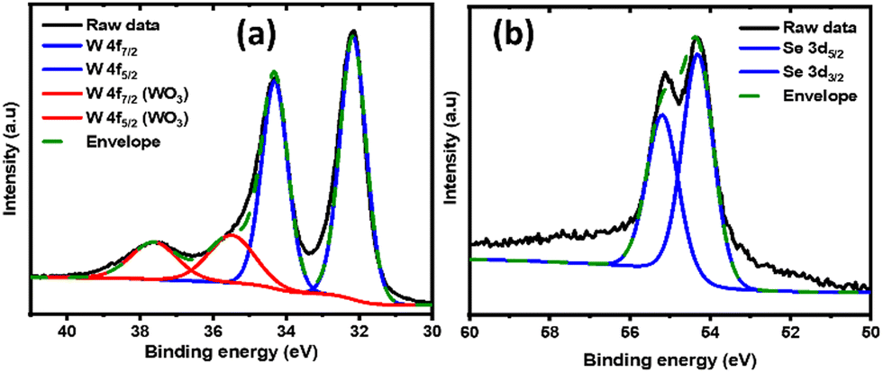 | ||
| Fig. 4 XPS measurements across the W (a) and Se (b) binding energy range for the WSe2 thin film. | ||
Raman spectroscopy is useful to probe the crystallinity and number of layers present in 2D TMDCs, allowing detection down to a single monolayer. It has been employed in this study to probe the quality of electrodeposited WSe2 thin films by confirming the presence of signature Raman peaks of WSe2 and by comparing the full-width at half maximum (FWHM) of the peaks. Fig. 5 shows the Raman spectra recorded from both the as-deposited and the annealed WSe2 thin films. The as-deposited WSe2 film shows a broad peak at 252 cm−1, consistent with the partial crystallinity of the thin film before annealing, with FWHM = 35 cm−1. After ‘flash’ annealing, the main Raman peak at 252 cm−1 becomes much sharper and the FWHM reduces to 14 cm−1, indicating significantly increased crystallinity and long-range layer ordering, and in agreement with the STEM data. The sharp peak at 252 cm−1, corresponding to the overlapping in-plane (E12g) and out-of-plane (A1g) vibrational modes of crystalline WSe2, is in good agreement with the literature.53,54 The E12g and A1g vibrational modes have essentially the same frequency, which restricts identification of the two contributions to the main peak.55 In addition to the main peak, several lower intensity peaks became apparent after annealing. The weak Raman peak at 306 cm−1 corresponds to the B12g mode, which is related to the interlayer interactions.52 The three minor peaks observed at 358, 372 and 394 cm−1 correspond to the 2E1g, A1g+LA and 2A1g-LA second order vibrational modes of WSe2.56 Their presence can be used as an indicator of the crystalline quality of the WSe2, whereas the as-deposited films only show the main Raman peak at 252 cm−1.
 | ||
| Fig. 5 Raman spectra recorded from the as-deposited and annealed WSe2 thin films using 532 nm laser excitation. | ||
Electrodeposition of WSe2 films from a TiN nanoband electrode across an insulating SiO2 surface
To evaluate the suitability of the electrodeposited WSe2 thin films for future device application, it is important to characterise the electrical properties of the material. However, as mentioned earlier, since electrodeposition is usually onto a conducting substrate, this precludes direct electrical characterization, because the conducting electrode dominates the electrical response. Therefore, we have employed a nanoband electrode structure, similar to that used for 2D-MoS2 deposition in our previous work,34 to electrodeposit the WSe2 thin films over an insulating SiO2 surface. The concept of promoting anisotropic 2D growth of WSe2 by employing a combination of the SSP (WSeCl4) and the TiN nanoband electrode is illustrated in Fig. 6a. Microfabricated arrays with TiN nanoband electrodes (100 nm thick) are used to initiate WSe2 nucleation and growth from the edges of the nanoband electrode and to drive the growth out across the SiO2. Various gaps between the pairs of TiN nanoband electrodes were fabricated (2, 4, 6 and 8 μm), so that the electrodeposition could be controlled to obtain the required growth lengths. Pulsed electrodeposition was performed by holding the electrode at −1.4 V for 5 s and 0 V for 3 s over 540 cycles so that the total time of active pulses is 45 min. Fig. 6b shows an optical microscope image of the microelectrode arrays after the electrodeposition. The blue-coloured material at the edges and over the (SiO2) microchannels indicates that all the channels are covered with WSe2 after the electrodeposition experiment. Annealing was performed (700 °C in vacuo for 10 min) before performing the electrical measurements. Micro-Raman measurements also confirm that the deposited material in all of the channels is WSe2 (Fig. 6c). | ||
| Fig. 6 (a) An illustration of the concept of 2D anisotropic growth of WSe2 over the SiO2/Si substrate from the TiN nanoband electrodes that are top covered with a SiO2 insulator. (b) Optical microscope image showing the 2, 4, 6 and 8 μm channels filled with the electrodeposited WSe2 films (bluish coloured regions). (c) Raman spectra recorded from the different electrode channels. (d) Current–voltage sweeps from the WSe2 deposited on different channels. | ||
Electrical characterization of the WSe2 films was then undertaken by connecting adjacent electrodes to a semiconductor device analyser. Fig. 6d shows the output characteristics measured from WSe2 in the 2, 4, 6 and 8 μm channels, respectively with the obtained IV characteristics exhibiting ohmic (linear) behaviour. Based on these measurements, the resistance value for 2 μm channel is 1.52 × 10⁵ Ω. Considering the TiN nanoband length of 177.5 μm, and the WSe2 thickness of 25 nm from AFM measurements, we estimated the resistivity of the electrodeposited WSe2 at room temperature as 34 Ω cm. This is slightly higher than typical reported values (5 Ω cm) for WSe2 synthesised by solvothermal approach,57 solid-state reaction58 and chemical vapor transport.59 This higher resistivity may be attributed to the grain boundary caused by the merging of the WSe2 films grown from either side of the channel.60–62 As evidenced by TEM, our grains are only 30 nm long on average, leading to substantial scattering across the film. The measured resistance values of the 4, 6 and 8 μm channels are much higher in comparison to that of the 2 μm channel, (4.88 × 10⁷ Ω for the 4 μm channel, 2.01 × 10⁸ Ω for the 6 μm channel and 2.44 × 10⁸ Ω for the 8 μm channel) indicating that WSe2 has not connected fully across the insulating SiO2 channel, consistent with these larger gaps requiring longer deposition times to fully contact the material grown from both sides. The anisotropic 2D growth and the electrical properties of WSe2 demonstrate the potential of the electrodeposition method as an alternative, transfer-free process to deposit TMDC materials for device applications.
Conclusions
We have successfully demonstrated the electrodeposition of 2D layered WSe2 in acetonitrile using WSeCl4 as a single source precursor. Pulsed electrodeposition was carried out for the deposition of WSe2 resulting in thin films with a flat and smooth morphology across the electrode surface. The electrodeposition produces laminar growth of WSe2 thin films formed of polycrystalline/nanocrystalline WSe2, which crystallises fully upon annealing. The compositional and structural quality of the WSe2 deposits were confirmed by SEM, STEM, EDS, X-ray diffraction, XPS, and Raman spectroscopic analysis.We have also demonstrated the use of WSeCl4 for the electrodeposition of WSe2 films from TiN nanoband electrodes over an insulating substrate for the first time as a proof-of-concept, and to allow the direct (transfer-free) measurement of electrical characteristics.
This study shows that electrodeposition from a single source precursor provides a viable alternative technique for the deposition of WSe2 and thus opens up future prospects for combining electrochemically deposited TMDC materials to achieve 2D heterostructures.
Future work will investigate the speciation of WSeCl4 in MeCN in order to understand the electrochemical mechanism occurring in this electrolyte. Further studies will also focus on controlling the WSe2 layer thickness and improving the crystallinity of the as-deposited WSe2 films, for example, by further optimising the electrodeposition potential, the electrolyte concentration or the pulsing sequence. Modifying the fabrication process of the nanoband electrodes to reduce the thickness of the TiN further is also expected to increase the control of the electrochemical nucleation, increase the uniformity and promote in-plane 2D growth. It is expected that these studies will also have a favourable effect on the electronic properties of the electrodeposited WSe2 films.
Author contributions
All authors discussed and contributed to the interpretation of the results and the final manuscript. S. T. and V. K. G. planned the experiments. S. T., V. K. G., J. Z. and N. Z. prepared the samples and carried out the experiments. G. R., P. N. B. and K. D. G. supervised the project. Y. J. N and N. M. A. helped supervise the project and the analysis of data. R. B., Y. H. and S. R. performed characterization and analysis of materials. S. T. wrote the manuscript with support from V. K. G.Data availability
The data supporting this article are provided in the ESI.†Conflicts of interest
There are no conflicts to declare.Acknowledgements
We thank the EPSRC for funding via EP/V062689/1, EP/V062387/1, EP/V062603/1, EP/V007629/1 and the Chemical Nanoanalysis Scanning Electron Microscope facility at the University of Southampton.References
- Q. H. Wang, K. Kalantar-Zadeh, A. Kis, J. N. Coleman and M. S. Strano, Nat. Nanotechnol., 2012, 7, 699–712 CrossRef CAS PubMed.
- A. Piacentini, A. Daus, Z. Wang, M. C. Lemme and D. Neumaier, Adv. Electron. Mater., 2023, 9, 2300181 CrossRef CAS.
- K. F. Mak, C. Lee, J. Hone, J. Shan and T. F. Heinz, Phys. Rev. Lett., 2010, 105, 136805 CrossRef PubMed.
- A. Chaves, J. G. Azadani, H. Alsalman, D. R. da Costa, R. Frisenda, A. J. Chaves, S. H. Song, Y. D. Kim, D. He, J. Zhou, A. Castellanos-Gomez, F. M. Peeters, Z. Liu, C. L. Hinkle, S.-H. Oh, P. D. Ye, S. J. Koester, Y. H. Lee, P. Avouris, X. Wang and T. Low, npj 2D Mater. Appl., 2020, 4, 29 CrossRef CAS.
- H. Zhou, C. Wang, J. C. Shaw, R. Cheng, Y. Chen, X. Huang, Y. Liu, N. O. Weiss, Z. Lin, Y. Huang and X. Duan, Nano Lett., 2015, 15, 709–713 CrossRef CAS PubMed.
- Y.-Z. Zhang, G.-J. Zhu and J.-H. Yang, Nanoscale, 2023, 15, 12116–12122 RSC.
- C.-H. Lee, G.-H. Lee, A. M. van der Zande, W. Chen, Y. Li, M. Han, X. Cui, G. Arefe, C. Nuckolls, T. F. Heinz, J. Guo, J. Hone and P. Kim, Nat. Nanotechnol., 2014, 9, 676–681 CrossRef CAS PubMed.
- T. Yang, B. Zheng, Z. Wang, T. Xu, C. Pan, J. Zou, X. Zhang, Z. Qi, H. Liu, Y. Feng, W. Hu, F. Miao, L. Sun, X. Duan and A. Pan, Nat. Commun., 2017, 8, 1906 CrossRef PubMed.
- X. Li, P. Zhou, X. Hu, E. Rivers, K. Watanabe, T. Taniguchi, D. Akinwande, J. S. Friedman and J. A. C. Incorvia, ACS Nano, 2023, 17, 12798–12808 CrossRef CAS PubMed.
- Y. Shingaya, A. Zulkefli, T. Iwasaki, R. Hayakawa, S. Nakaharai, K. Watanabe, T. Taniguchi and Y. Wakayama, Adv. Electron. Mater., 2023, 9, 2200704 CrossRef CAS.
- H. Fang, S. Chuang, T. C. Chang, K. Takei, T. Takahashi and A. Javey, Nano Lett., 2012, 12, 3788–3792 CrossRef CAS PubMed.
- A. Di Bartolomeo, F. Urban, M. Passacantando, N. McEvoy, L. Peters, L. Iemmo, G. Luongo, F. Romeo and F. Giubileo, Nanoscale, 2019, 11, 1538–1548 RSC.
- H. Li, J. Wu, Z. Yin and H. Zhang, Acc. Chem. Res., 2014, 47, 1067–1075 CrossRef CAS PubMed.
- H. Zhou, C. Zhang, A. Gao, E. Shi and Y. Guo, Chem. Commun., 2024, 60, 943–955 RSC.
- M. Nakano, Y. Wang, Y. Kashiwabara, H. Matsuoka and Y. Iwasa, Nano Lett., 2017, 17, 5595–5599 CrossRef CAS PubMed.
- S. Seo, H. Choi, S.-Y. Kim, J. Lee, K. Kim, S. Yoon, B. H. Lee and S. Lee, Adv. Mater. Interfaces, 2018, 5, 1800524 CrossRef.
- H. Li, D. Gao, S. Xie and J. Zou, Sci. Rep., 2016, 6, 36451 CrossRef CAS PubMed.
- J. M. Velazquez, F. H. Saadi, A. P. Pieterick, J. M. Spurgeon, M. P. Soriaga, B. S. Brunschwig and N. S. Lewis, J. Electroanal. Chem., 2014, 716, 45–48 CrossRef CAS.
- W. Jung, S. Lee, D. Yoo, S. Jeong, P. Miró, A. Kuc, T. Heine and J. Cheon, J. Am. Chem. Soc., 2015, 137, 7266–7269 CrossRef CAS PubMed.
- B.-Q. Zhang, J.-S. Chen, H.-L. Niu, C.-J. Mao and J.-M. Song, Nanoscale, 2018, 10, 20266–20271 RSC.
- D. Chakravarty and D. J. Late, RSC Adv., 2015, 5, 21700–21709 RSC.
- V. K. Greenacre, A. L. Hector, R. Huang, W. Levason, V. Sethi and G. Reid, Dalton Trans., 2022, 51, 2400–2412 RSC.
- B. Liu, M. Fathi, L. Chen, A. Abbas, Y. Ma and C. Zhou, ACS Nano, 2015, 9, 6119–6127 CrossRef CAS PubMed.
- P. N. Bartlett, S. L. Benjamin, C. H. de Groot, A. L. Hector, R. Huang, A. Jolleys, G. P. Kissling, W. Levason, S. J. Pearce, G. Reid and Y. Wang, Mater. Horiz., 2015, 2, 420–426 RSC.
- K. Cicvarić, L. Meng, D. W. Newbrook, R. Huang, S. Ye, W. Zhang, A. L. Hector, G. Reid, P. N. Bartlett and C. H. K. de Groot, ACS Omega, 2020, 5, 14679–14688 CrossRef PubMed.
- S. Murugesan, A. Akkineni, B. P. Chou, M. S. Glaz, D. A. Vanden Bout and K. J. Stevenson, ACS Nano, 2013, 7, 8199–8205 CrossRef CAS PubMed.
- T. Manyepedza, T. Auvray, T. Friščić and N. V. Rees, Electrochem. Commun., 2024, 160, 107678 CrossRef CAS.
- P. C. Andricacos, Electrochem. Soc. Interface, 1999, 8, 32 CrossRef CAS.
- A. S. Aliyev, M. Elrouby and S. F. Cafarova, Mater. Sci. Semicond. Process., 2015, 32, 31–39 CrossRef CAS.
- S. Thomas, D. E. Smith, V. K. Greenacre, Y. J. Noori, A. L. Hector, C. H. d Groot, G. Reid and P. N. Bartlett, J. Electrochem. Soc., 2020, 167, 106511 CrossRef CAS.
- Y. J. Noori, S. Thomas, S. Ramadan, D. E. Smith, V. K. Greenacre, N. Abdelazim, Y. Han, R. Beanland, A. L. Hector, N. Klein, G. Reid, P. N. Bartlett and C. H. Kees de Groot, ACS Appl. Mater. Interfaces, 2020, 12, 49786–49794 CrossRef CAS PubMed.
- S. Thomas, V. K. Greenacre, D. E. Smith, Y. J. Noori, N. M. Abdelazim, A. L. Hector, C. H. de Groot, W. Levason, P. N. Bartlett and G. Reid, Chem. Commun., 2021, 57, 10194–10197 RSC.
- Y. J. Noori, S. Thomas, S. Ramadan, V. K. Greenacre, N. M. Abdelazim, Y. Han, J. Zhang, R. Beanland, A. L. Hector, N. Klein, G. Reid, P. N. Bartlett and C. H. de Groot, 2D Mater., 2022, 9, 015025 CrossRef CAS.
- N. M. Abdelazim, Y. J. Noori, S. Thomas, V. K. Greenacre, Y. Han, D. E. Smith, G. Piana, N. Zhelev, A. L. Hector, R. Beanland, G. Reid, P. N. Bartlett and C. H. de Groot, Adv. Electron. Mater., 2021, 7, 2100419 CrossRef CAS.
- S. M. Delphine, M. Jayachandran and C. Sanjeeviraja, Mater. Chem. Phys., 2003, 81, 78–83 CrossRef CAS.
- J. Jebaraj Devadasan, C. Sanjeeviraja and M. Jayachandran, Mater. Chem. Phys., 2003, 77, 397–401 CrossRef CAS.
- S. Gawale, R. Mane, A. Sargar, S. Mane, R. Kharade and P. Bhosale, J. Arch. Appl. Sci. Res., 2010, 2, 218–224 CAS.
- D. E. Smith, V. K. Greenacre, A. L. Hector, R. Huang, W. Levason, G. Reid, F. Robinson and S. Thomas, Dalton Trans., 2020, 49, 2496–2504 RSC.
- D. Britnell, G. W. A. Fowles and D. A. Rice, J. Chem. Soc., Dalton Trans., 1974, 2191–2194, 10.1039/DT9740002191.
- W. Levason, G. Reid, D. E. Smith and W. Zhang, Polyhedron, 2020, 179, 114372 CrossRef CAS.
- V. K. Greenacre, A. L. Hector, W. Levason, G. Reid, D. E. Smith and L. Sutcliffe, Polyhedron, 2019, 162, 14–19 CrossRef CAS.
- M. G. B. Drew and R. Mandyczewsky, J. Chem. Soc. A, 1970, 2815–2818, 10.1039/J19700002815.
- F. A. Cotton, P. A. Kibala and R. B. W. Sandor, Inorg. Chem., 1989, 28, 2485–2487 CrossRef CAS.
- K. H. Moock, S. A. Macgregor, G. A. Heath, S. Derrick and R. T. Boeré, J. Chem. Soc., Dalton Trans., 1996, 2067–2076, 10.1039/DT9960002067,.
- G. Sauerbrey, Z. Phys., 1959, 155, 206–222 CrossRef CAS.
- P.-C. Wu, C.-L. Yang, Y. Du and C.-H. Lai, Sci. Rep., 2019, 9, 8017 CrossRef PubMed.
- J. A. Champion, Br. J. Appl. Phys., 1965, 16, 1035 CrossRef CAS.
- N. D. Boscher, C. J. Carmalt and I. P. Parkin, J. Mater. Chem., 2006, 16, 122–127 RSC.
- J. Huang, L. Yang, D. Liu, J. Chen, Q. Fu, Y. Xiong, F. Lin and B. Xiang, Nanoscale, 2015, 7, 4193–4198 RSC.
- M. S. Sokolikova, P. C. Sherrell, P. Palczynski, V. L. Bemmer and C. Mattevi, Nat. Commun., 2019, 10, 712 CrossRef CAS PubMed.
- H. Wang, D. Kong, P. Johanes, J. J. Cha, G. Zheng, K. Yan, N. Liu and Y. Cui, Nano Lett., 2013, 13, 3426–3433 CrossRef CAS PubMed.
- J.-K. Huang, J. Pu, C.-L. Hsu, M.-H. Chiu, Z.-Y. Juang, Y.-H. Chang, W.-H. Chang, Y. Iwasa, T. Takenobu and L.-J. Li, ACS Nano, 2014, 8, 923–930 CrossRef CAS PubMed.
- H. Zeng, G.-B. Liu, J. Dai, Y. Yan, B. Zhu, R. He, L. Xie, S. Xu, X. Chen, W. Yao and X. Cui, Sci. Rep., 2013, 3, 1608 CrossRef PubMed.
- P. M. Pataniya, M. Tannarana, C. K. Zankat, S. A. Bhakhar, S. Narayan, G. K. Solanki, K. D. Patel, P. K. Jha and V. M. Pathak, J. Phys. Chem. C, 2020, 124, 2251–2257 CrossRef CAS.
- E. del Corro, H. Terrones, A. Elias, C. Fantini, S. Feng, M. A. Nguyen, T. E. Mallouk, M. Terrones and M. A. Pimenta, ACS Nano, 2014, 8, 9629–9635 CrossRef CAS PubMed.
- H. Li, G. Lu, Y. Wang, Z. Yin, C. Cong, Q. He, L. Wang, F. Ding, T. Yu and H. Zhang, Small, 2013, 9, 1974–1981 CrossRef CAS PubMed.
- M. Kaur, K. Singh, I. Chauhan, H. Singh, R. K. Sharma, A. Vij, A. Thakur and A. Kumar, J. Alloys Compd., 2021, 869, 159369 CrossRef CAS.
- M. Alzaid, N. M. A. Hadia, E. R. Shaaban, M. El-Hagary and W. S. Mohamed, Appl. Phys. A: Mater. Sci. Process., 2022, 128, 94 CrossRef CAS.
- A. Klein, P. Dolatzoglou, M. Lux-Steiner and E. Bucher, Sol. Energy Mater. Sol. Cells, 1997, 46, 175–186 CrossRef CAS.
- Y. Shi, H. Li and L.-J. Li, Chem. Soc. Rev., 2015, 44, 2744–2756 RSC.
- H. Ago, S. Fukamachi, H. Endo, P. Solís-Fernández, R. Mohamad Yunus, Y. Uchida, V. Panchal, O. Kazakova and M. Tsuji, ACS Nano, 2016, 10, 3233–3240 CrossRef CAS PubMed.
- H. Schmidt, F. Giustiniano and G. Eda, Chem. Soc. Rev., 2015, 44, 7715–7736 RSC.
Footnote |
| † Electronic supplementary information (ESI) available. See DOI: https://doi.org/10.1039/d4tc02755h |
| This journal is © The Royal Society of Chemistry 2024 |