
 Open Access Article
 This Open Access Article is licensed under a Creative Commons Attribution-Non Commercial 3.0 Unported Licence
Confined deep red light-detecting organic phototransistors with polymer gate-sensing layers consisting of indacenothiophene and dinitrobenzothiadiazole units†
Chanbin
Park
ab,
Taehoon
Kim
a,
Hwajeong
Kim
ac and
Youngkyoo
Kim
 *ab
*ab
aOrganic Nanoelectronics Laboratory and KNU Institute for Nanophotonics Applications (KINPA), Department of Chemical Engineering, School of Applied Chemical Engineering, Kyungpook National University, Daegu 41566, Republic of Korea. E-mail: ykimm@knu.ac.kr
bDepartment of Energy Convergence & Climate Change and Institute for Global Climate Change and Energy, Kyungpook National University, Daegu 41566, Republic of Korea
cPriority Research Center, Research Institute of Environmental Science & Technology, Kyungpook National University, Daegu 41566, Republic of Korea
First published on 3rd September 2024
Abstract
Here we report a novel conjugated polymer with deep red-light absorption, consisting of indacenothiophene (IDTT) and dinitrobenzothiadiazole (DNBT) units, which can be used as a gate-sensing layer (GSL) in organic phototransistors (OPTRs). The PIDTT–DNBT polymer was synthesized by the Stille coupling reaction between the IDTT monomer with tin end groups and the DNBT monomer with bromine end groups. The PIDTT–DNBT films showed two pronounced optical absorptions in the wavelength (λ) ranges of 350–470 nm and 470–800 nm and the highest occupied molecular orbital (HOMO) energy of −5.9 eV. The OPTRs with the PIDTT–DNBT GSLs operated in p-channel modes and exhibited noticeable photo-sensing performances under the illumination of three monochromatic lights (λ = 550, 670, and 700 nm). When visible light-cutting layers (VLCLs) were applied, the OPTRs with the PIDTT–DNBT GSLs could only sense deep-red light with a narrow spectral range of λ = 650–800 nm in the absence of other visible light interferences.
Introduction
Organic phototransistors (OPTRs), acting as photosensors by converting incident photons into electrical signals, have received considerable attention because of their potential for ultrathin and flexible photosensor modules.1–7 Basically, OPTRs employ the geometry of organic field-effect transistors (OFETs) with three electrodes that control the charge transport of organic channel layers.8–12 As organic channel layers in typical OPTRs play dual roles of enabling charge transport and photo-detection, organic materials for the channel layers need good semiconducting properties.13–15 On account of this fact, among various organic materials, conjugated polymers have been extensively studied for the channel layers due to their delocalized pi-orbital structures that can exhibit both charge transport and light absorption characteristics.16–18Recently, deep red light, corresponding to a wavelength (λ) range of 650–750 nm, has been an important medium for various applications, including skin therapeutic devices, because its longest wavelength among all the visible light wavelengths endows it with the highest penetration depth.19–23 To control the deep red light in systems, OPTRs can be used as photosensors due to their scalability for various shapes.24,25 However, a limited number of conjugated polymers can have optical absorption in the deep red light range, even though most conjugated polymers show partial light absorption in the visible light range (λ = 400–750 nm).26–28 The conjugated polymers, which can absorb deep red light, can be achieved by either extending conjugation lengths or combining comonomers in chains.29–31
In particular, it has been reported that the optical absorption range is controllable by the combination of electron-donating comonomers and electron-accepting comonomers because of the energy gap change between the highest occupied molecular orbital (HOMO) and the lowest unoccupied molecular orbital (LUMO) energy levels.32–34 As the representative electron-accepting comonomers for the synthesis of visible light-absorbing conjugated polymers, benzothiadiazole (BT) derivatives have been extensively used in combination with various electron-donating comonomers including indacenodithienothiophene (IDTT) derivatives.35–40 However, the optical absorption range of the IDTT/BT-based polymer (PIDTT–BT) could not fully cover the deep red light range (maximum peak at λ = 638 nm), owing to considerably low absorption at around 700 nm (almost no absorption at λ = 750 nm), so the PIDTT–BT polymer cannot be applied for sensing the full range of deep red light.41
In this work, to achieve a red-shifted optical absorption, we introduced a dinitrobenzothiadiazole (DNBT) comonomer to polymerize with the IDTT comonomer because the two nitro groups provide the BT core with further increased electron-accepting characteristics. The resulting polymer, poly(5,5,11,11-tetrakis(5-(2-ethylhexyl)-thiophene-2-yl)-dithieno[2,3-d:2′,3′-d′]-s-indaceno[1,2-b:5,6-b′]-dithiophene-co-5,6-dinitrobenzo[1,2,5]thiadiazole) (PIDTT–DNBT), exhibited enhanced optical absorption (film) in the deep red light range with the maximum peak at λ = 670 nm and the absorption edge up to 900 nm. The PIDTT-DNBT films were applied as a gate-sensing layer (GSL) in the OPTRs to separate their role from channel layers. In particular, an approach for sensing well-confined deep red light without a disturbance of any other visible light was attempted by employing a visible light-cutting layer (VLCL) made with thick poly(3-hexylthiophene) (P3HT) films that can only pass the deep red light part among the whole visible light. The OPTRs with the PIDTT–DNBT GSLs showed typical p-channel transistor behaviors and could sense a wide range of visible light wavelengths, while the OPTRs with additional VLCLs exhibited confined detection of deep red light only.
Results and discussion
As shown in Fig. 1a, the PIDTT–DNBT polymer was synthesized by the Stille coupling reaction between 3,9-bis(trimethylstannane)-5,5,11,11-tetrakis(5-(2-ethylhexyl)-thiophene-2-yl)-dithieno[2,3-d:2′,3′-d′]-s-indaceno[1,2-b:5,6-b′]-dithiophene (2Sn-IDTT) and 4,7-dibromo-5,6-dinitrobenzo[1,2,5]thiadiazole (2Br-DNBT) in the presence of a phosphine/palladium catalyst at 100 °C for 24 h (see the Experimental section for the detailed procedures). The pristine PIDTT–DNBT solution exhibited two distinct optical absorptions in the wavelength (λ) range of 350–470 nm and 470–800 nm (see Fig. 1b). A similar optical absorption spectrum was measured for the PIDTT–DNBT film but the peak at λ = 470–800 nm (maximum at λ = 670 nm) was slightly broadened compared to that of the solution. As illustrated in Fig. 1c, the PIDTT–DNBT layers were placed as GSLs between the PMMA gate-insulating layer (GIL) and the ITO gate electrode on the bottom of the substrate. Note that the PIDTT–DNBT polymer (solid) was thermally stable up to ca. 260 °C (see Fig. S1a, ESI†). To investigate the GSL thickness effect, the PIDTT–DNBT layers with three different thicknesses (t = 40, 80, 120 nm) were coated on the ITO-glasses. To cut the incoming visible light with wavelengths shorter than the deep red light, the 900 nm-thick VLCL (P3HT film) was first coated on the front side of the ITO-glasses before coating other layers and depositing source/drain electrodes. Because the VLCL has very high absorbance (i.e., extremely low transmittance), the visible light below λ = ca. 650 nm could be almost blocked (see very low transmittance in Fig. 1d and an absorption spectrum of typical thin P3HT film in Fig. S1b, ESI†). Note that the transmittance of the P3HT VLCL was 0.04% at λ = 550 nm, 31.28% at λ = 670 nm, and 63.16% at λ = 700 nm. Consequently, the PIDTT–DNBT GSLs in devices could absorb light with a narrow spectral range of λ = ca. 650–800 nm, which passed through the P3HT VLCL. A close investigation can find that the major absorption part of the filtered spectrum by the VLCL is located in the deep red region (λ = 650–750 nm), together with a minor absorption in the near-infrared edge (λ = 750–800 nm), featuring the full-width at half-maximum (FWHM) of ca. 87 nm (see Fig. 1e). | ||
| Fig. 1 (a) Synthesis scheme for the PIDTT–DNBT polymer via Stille coupling reactions of 2Sn-IDTT and 2Br-DNBT in the presence of catalysts. (b) Optical absorption spectra of the PIDTT–DNBT solution (solvent: chlorobenzene) and film (t = 80 nm) (inset: photographs for the solution and film). (c) Illustration of the structure of OPTRs with the PIDTT–DNBT GSLs and P3HT VLCLs. (d) Optical transmission spectrum of the P3HT VLCL (t = 900 nm) compared to the absorption spectrum of the PIDTT–DNBT film (t = 80 nm). (e) Optical absorption spectrum of the glass/ITO/PIDTT–DNBT sample after filtering the absorption of the P3HT VLCL (note that the full width at half maximum (FWHM) was calculated to be 87 nm). | ||
The molecular orbital energy levels of PIDTT–DNBT films were characterized by ultraviolet photoelectron spectroscopy (UPS). As observed from the UPS spectra in Fig. 2a, the onset energy of the valence region (EV) was measured at ca. 3.23 eV, and the inflection point of the cut-off region (ECO) was obtained at 18.53 eV. Here, the HOMO energy (EHOMO) was calculated to be −5.9 eV from the relation of EHOMO = −[hv − (ECO + EV)], where hv represents the incident photon energy (21.2 eV) of the UPS measurement system. The Tauc plot of the optical absorption spectrum (see Fig. S2, ESI†) showed the optical energy gap (Eg) of ca. 1.64 eV for the PIDTT–DNBT film. Consequently, the LUMO energy (ELUMO) of −4.26 eV was obtained from the Eg and HOMO energy values (Eg = EHOMO − ELUMO). Based on the HOMO–LUMO energy levels of PIDTT–DNBT films, the energy level (band) diagram of the present device is constructed as displayed in Fig. 2b. Because the PIDTT–DNBT film (t = 80 nm) acts as a GSL below the 450 nm-thick PMMA GIL, a huge electrical leakage between the source and gate electrodes is not considered under gate bias conditions for transistor operations.
 | ||
| Fig. 2 (a) UPS spectrum of the PIDTT–DNBT film coated on a glass substrate (inset: enlarged part focusing on the valence region). ECO and EV denote the energy of the cutoff (midpoint) and valence (onset) regions, respectively. (b) Flat energy level (band) diagram of the OPTR device between the source and gate electrodes. | ||
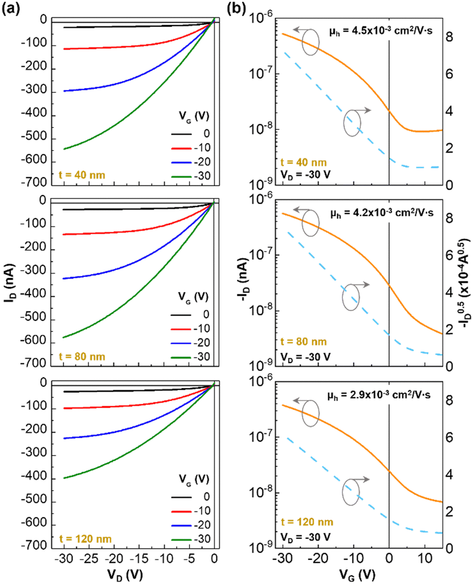
Next, the transistor performances were measured in the dark to examine whether the present devices with the PIDTT–DNBT GSLs function properly in field-effect modes. As observed from the output curves in Fig. 3a, all devices exhibited p-channel transistor characteristics with a saturation behavior. The drain current (ID) level noticeably jumped with the increased gate voltage (VG) irrespective of the thickness of PIDTT–DNBT GSLs. However, the highest drain current at the same gate and drain voltages was obtained at t = 80 nm. This result can be attributed to the trade-off between the number of photo-generated excitons and the finally separated number of charges from the excitons. As the GSL thickness increased from t = 40 nm to 120 nm, the population of the excitons generated by optical absorption increased gradually. However, the number of charges (holes and electrons) separated from the photo-generated excitons might be reduced because of the weakened power of exciton dissociation owing to the decreased electric field at the thicker GSLs in the case of the same VG. Hence, the 80 nm-thick PIDTT–DNBT GSLs could deliver the highest ID in the present structure of transistors. The transfer curves in Fig. 3b confirm the appropriate operation of devices in the p-channel mode when it comes to the gradually increased drain current (negatively) by the negative increase of gate voltage. Similar to the trend of output curves, the highest drain current was measured together with the relatively low off-current level at t = 80 nm. From the ID0.5–VG plots, the hole mobility (μh) of devices was calculated using the slope in the saturation-regime equation, μh = [2L·ID,sat]/[W·CGIL·(VG − VTH)2], where ID,sat, W, L, CGIL, and VTH represent the drain current in the saturated region, channel width, channel length, capacitance of GIL, and threshold voltage, respectively. All the devices showed quite a similar level of hole mobility in the range of 2.9–4.5 × 10⁻³ cm2 V−1 s−1, indicative of a weak thickness influence of PIDTT–DNBT GSLs.
 | ||
| Fig. 3 (a) Output and (b) transfer curves in the dark for the OPTRs with the PIDTT–DNBT GSLs (t = 40, 80, and 120 nm). The hole mobility (μh) calculated from the slope of ID0.5–VG plots is given on each graph of the transfer curves. | ||
To further investigate the thickness effect, the surface morphology of the PIDTT–DNBT layers was examined using atomic force microscopy (AFM). As compared in Fig. 4a, all the layers showed a featureless random morphology with a similar level of root-mean-square roughness (Rg = 0.53–0.68 nm). Thus, these random surfaces of the three PIDTT–DNBT films might deliver an environment to form similar interfaces with the PMMA layers in the transistors, leading to an analogous level of hole mobility (2.9–4.5 × 10⁻³ cm2 V−1 s−1) in the P3HT channel layers.
 | ||
| Fig. 4 (a) Height-mode AFM images of the PIDTT–DNBT films according to the film thickness (see the root-mean-square roughness (Rg) on the bottom of each image). (b) and (c) 2D wide-angle X-ray scattering (GIWAXS) images (b) and 1D profiles (c) of the PIDTT–DNBT films: OOP and IP denote the out-of-plane and in-plane directions in the films, respectively. Note that the 1D profile at 45° was obtained by the extraction of scattering data at the azimuthal angle of 45° in the 2D image (see Y. Kim et al., Soft Mater., 2007, 3, 117). | ||
The nanostructure investigation by the synchrotron radiation-grazing incidence wide-angle X-ray scattering (GIWAXS) method disclosed that the PIDTT–DNBT film (t = 80 nm) has a broad Debye–Scherrer ring (at a scattering vector of qxy = qz = 0.3–0.4 Å−1) with a relatively intense diffraction intensity in the out-of-plane (OOP) direction (see the two-dimensional (2D) image in Fig. 4b). In addition, a part of another diffraction ring was measured at qxy = 0.31 Å−1, which is relatively pronounced in the in-plane (IP) direction. These diffractions in the 2D images were further analyzed based on the corresponding one-dimensional (1D) profiles. Here, considering that the reflected X-ray beams affected the diffraction signals at such low angles, the 1D profiles at an azimuthal angle of 45° were compared with those in the OOP and IP directions. As plotted in Fig. 4c, the diffraction peaks at qxy = qz = 0.3–0.4 Å−1 can be assigned to the (100) stacking of PIDTT–DNBT chains when it comes to the d-spacing value of ca. 2.03 nm. As observed in the 2D image, the diffraction peak at qxy = 0.95–0.97 Å−1 was found in the IP direction despite a quite small bump only in the OOP direction. This peak with the d-spacing of ca. 0.67 nm can be allocated to the (010) stacking of PIDTT–DNBT chains (see the energy minimized molecular structure and illustrated chain stacking in Fig. S3, ESI†). Note that similar GIWAXS results were obtained for other thicknesses (see Fig. S4, ESI†). The loosely stacked chain structure of PIDTT–DNBT, indicative of poor pi-electron transfer through polymer chains, might be responsible for its inability to act as a channel layer but could have a high capability as a GSL in the present transistor structure.
Based on the transistor performances in the dark, the devices with the 80 nm-thick PIDTT–DNBT GSLs were chosen for the investigation of photo-sensing characteristics. The photo-sensing performances of devices were first investigated by illuminating three different monochromatic lights (λ = 550, 670, and 700 nm) on the glass side of devices without the VLCLs. As shown in Fig. 5a, the drain current of output curves noticeably increased upon monochromatic light illumination irrespective of the wavelength. However, the largest increase in drain current was measured at λ = 550 nm, compared to the other two wavelengths (λ = 670 and 700 nm), even though the incident light intensity (PIN) was lower, 162 μW cm−2 at λ = 550 nm, than 277 μW cm−2 (λ = 670 nm) and 281 μW cm−2 (λ = 700 nm). The reason can be attributed to the role of the P3HT CLs that should absorb photons of λ = 550 nm but did not respond to those of the longer wavelengths. Considering the relatively low absorbance of PIDTT–DNBT films at λ = 550 nm compared to the other two wavelengths, the efficiency of photo-induced current generation might be higher in the P3HT CLs than that in the PIDTT–DNBT GSLs. Therefore, the increased drain current at λ = 670 and 700 nm can be solely assigned to the action of the PIDTT–DNBT GSLs. A similar increase in drain current upon monochromatic light illumination was measured from the transfer curves (see Fig. 5b). The net drain current without VLCLs (t = 40 and 120 nm) between dark and light illumination conditions from output curves also shows a similar tendency (see Fig. S5 and S6, ESI†).
 | ||
| Fig. 5 (a) Output and (b) transfer curves of the PIDTT–DNBT-based OPTRs without the P3HT VLCLs under illumination with three different monochromatic lights. | ||
Additionally, the light illumination led to a noticeable shift in threshold voltage toward a positive direction of gate voltage, which was more pronounced at λ = 550 nm than at λ = 670 and 700 nm. This result implies that both GSLs and CLs influence the extent of threshold voltage shift. As a result, the photosensitivity (SP) and photoresponsivity (RC) in the deep red light range reached ca. 47% and 0.70 mA W−1 at λ = 670 nm and ca. 29% and 0.41 mA at λ = 700 nm, respectively (see Table 1). Note that a similar SP and RC trend was obtained in the case of the other two thicknesses (t = 40 and 120 nm) (see Table S1, ESI†). The photo-sensing performances at different drain and/or gate voltages are given in Fig. S7 (output curves) and S8 (transfer curves) (ESI†).
| Wavelength (nm) | S P (%) | R C (mA W−1) | ||
|---|---|---|---|---|
| w/o VLCL | w/VLCL | w/o VLCL | w/VLCL | |
| 550 | 86.0 | 0.52 | 2.13 | 0 |
| 670 | 46.9 | 38.6 | 0.70 | 0.68 |
| 700 | 28.9 | 24.8 | 0.41 | 0.40 |
Next, the photo-sensing performance of the OPTRs with the VLCLs was investigated under the illumination of the same three monochromatic lights used above. As shown in Fig. 6a, the drain current in the output curves was almost not changed under the green light illumination (λ = 550 nm) but increased certainly under the deep red-light illumination (λ = 670 and 700 nm) (see Fig. S9 for the drain current change, ESI†). Note that the drain current in the dark was relatively lower for the OPTRs with the VLCLs than those without the VLCLs because the ITO surfaces might be contaminated owing to the direct contact with the chuck of the spin-coater during the VLCL coating processes. The transfer curves in Fig. 6b showed that the drain current was unchanged at λ = 550 nm but increased at λ = 670 and 700 nm. In addition, the threshold voltage was not shifted at λ = 550 nm even though a noticeably shifted threshold voltage was measured at λ = 670 and 700 nm under the conditions of different drain/or gate voltages (see Fig. S10 for the transfer curve change, ESI†). This result indicates that the thick VLCLs could almost block the visible light part below λ = 650 nm and the present OPTRs could only detect the deep red part of visible light. The detailed analysis disclosed that the photosensitivity at λ = 670 nm was slightly reduced to SP = 38.6% (from 46.9% for the OPTRs without the VLCLs) owing to the marginal absorption by the spectral edge region of VLCLs (see Table 1). However, very small variations in the photosensitivity and photoresponsivity were measured in the case of λ = 700 nm, which can be attributable to the intrinsic effect of Fresnel reflection because of the increased number of interfaces.42 Note that the OPTRs with the VLCLs showed a similar trend even though different thicknesses were applied (see Fig. S11 and S12, ESI†).
 | ||
| Fig. 6 (a) Output and (b) transfer curves of the PIDTT–DNBT-based OPTRs with the P3HT VLCLs under illumination with three different monochromatic lights. | ||
Based on the above device results, the deep red light-sensing mechanism is proposed for the OPTRs with the PIDTT–DNBT GSLs and thick P3HT VLCLs (see Fig. 7). First, the field-effect charges are generated in the channel layer by applying negative voltages (VG < 0 V and VD < 0 V). Upon light illumination, only a deep red light can pass through the VLCL and make excitons in the PIDTT–DNBT GSL. Then, the excitons separate into individual charges (holes and electrons) with the assistance of an electric field between the source and gate electrodes. The separated charges induce holes in the P3HT CL across the PMMA GIL, which finally leads to the increased drain current.
 | ||
| Fig. 7 A mechanism proposed for the operation of the OPTRs with the PIDTT–DNBT GSLs and the P3HT VLCLs. ID,F and ID,L denote the drain current generated by the field effect and light illumination, respectively. | ||
Experimental section
Materials and solutions
2Sn-IDTT was purchased from Organtec (China), while 2Br-DNBT was supplied by AlfaChem (China). The catalysts, tri(o-tolyl)phosphine (P(o-tol)3) and tris(dibenzylideneacetone)dipalladium(0) (Pd2(dba)3), were purchased from Sigma-Aldrich (USA). PMMA (weight-average molecular weight = 120 kDa) and P3HT (weight-average molecular weight = 70 kDa, regioregularity >97%) were purchased from Sigma-Aldrich (USA) and Rieke Metals (Lincoln, NE, USA), respectively. Chlorobenzene, toluene, and n-butyl acetate were purchased from Sigma-Aldrich (USA). The P3HT solution for VLCLs and CLs was prepared by dissolving the P3HT powder in toluene at a concentration of 40 and 13 mg mL−1, respectively. The PMMA solution (80 mg mL−1) for GILs was prepared using n-butyl acetate as a solvent. The PIDTT–DNBT polymer for GSLs was prepared by dissolving the synthesized PIDTT–DNBT powder in chlorobenzene at various concentrations (8, 12, and 16 mg mL−1).Synthesis and characterization
The PIDTT–DNBT polymer was synthesized by reacting 2Sn-IDTT (1 M) and 2Br-DNBT (1 M), which were dissolved in chlorobenzene, via the Stille coupling mechanism in the presence of Pd2(dba)3 (2 mol%) and P(o-tol)3 (8 mol%) as catalysts. The reactants and catalysts were placed in a round-bottom pressure vessel charged with argon gas. The mixed solution was stirred at 100 °C for 24 h. Note that the initial color of 2Sn-IDTT and 2Br-DNBT was white and light yellow, respectively. As the reaction proceeded, the solution color turned deep blue. After 24 h, the reaction vessel was cooled down to room temperature. Then, the catalysts were filtered off using filter paper (pore size = 0.2 μm). Next, most solvents were dried off using a rotary evaporator to obtain the concentrated solutions. The concentrated solutions were slowly dropped into methanol leading to precipitation processes. After stirring for 2 h, the precipitates were filtered and dried in a vacuum oven at 40 °C for more than 24 h. The dried solid powder (PIDTT–DNBT) with a deep blue color delivered a synthesis yield of ca. 67%. The weight-average molecular weight of PIDTT–DNBT was measured to be ca. 184 kDa.Film and device fabrication
Indium-tin oxide (ITO)-coated glass substrates (ITO size = 1 mm × 12 mm) were prepared by photolithography processes and subjected to wet-cleaning processes using isopropyl alcohol and acetone in a sonication bath (30 min each). The cleaned ITO electrode-coated glass substrates were treated in a UV-ozone (UVO) environment for 20 min using a UVO cleaner (UV intensity = 28 mW cm−2). On the glass side of the ITO-glass substrates, the 900 nm-thick P3HT films as VLCLs were spin-coated and soft-baked at 80 °C for 20 min. Next, on the ITO-coated side of the ITO-glass substrates, the PIDTT–DNBT layers as GSLs were spin-coated and soft-baked at 80 °C for 20 min. The thickness of the PIDTT–DNBT layers (t = 40, 80, and 120 nm) was controlled by the concentration of solutions. Next, the PMMA solutions for 450 nm-thick GILs were spun on the GSL, followed by soft-baking at 80 °C for 30 min. Note that the PIDTT–DNBT layers were not damaged during the spin-coating process of PMMA layers because the PIDTT–DNBT polymer is insoluble in n-butyl acetate. Then, 50 nm-thick P3HT layers as CLs were spin-coated on the PMMA layers and subjected to soft-baking at 80 °C for 15 min. After moving these samples into a vacuum chamber system placed inside an argon-filled glovebox, silver (Ag) source/drain electrodes (t = 60 nm) were deposited on the P3HT CLs via thermal evaporation processes at a base pressure of ca. 1 × 10⁻⁶ Torr. The channel length and width of the final devices were 70 μm and 2 mm, respectively. All the fabricated devices were placed inside the argon-filled glove box to protect them from moisture and oxygen attacks.Measurement
A gel permeation chromatography system (GPC, Alliance e2695, Waters) was used to measure the molecular weight of PIDTT–DNBT. The optical absorption spectra of polymer solutions and films were measured using a UV-vis-NIR spectrophotometer (Lambda 750, PerkinElmer Inc.). The thermal degradation of polymers was carried out in a nitrogen environment using a thermogravimetric analyzer (TGA, Discovery SDT 650, TA Instruments). An ultraviolet photoelectron spectroscopy system (UPS, NEXSA XPS, Thermo Fisher Scientific) was used to measure the electronic structure of the PIDTT–DNBT film (He I, 21.2 eV) with an energy resolution of 0.05 eV. The thickness of polymer films and Ag electrodes was measured using a surface profilometer (DektakXT, Bruker). The surface morphology of film samples was examined using an atomic force microscope (AFM, NX20, Park Systems). The nanostructure of PIDTT–DNBT films was measured using a synchrotron-radiation GIWAXS (X-ray wavelength![[thin space (1/6-em)]](https://www.rsc.org/images/entities/char_2009.gif) =1.192Å) equipped at the 3C beamline in the Pohang Accelerator Laboratory (PAL). The performances of OFETs in the dark and under illumination were measured using a semiconductor parameter analyzer (Model 2636B, Keithley). To examine the phototransistor performances, the channel area of OPTRs was carefully illuminated with the three monochromatic lights (λ = 550, 670, and 700 nm) that were filtered from a tungsten-halogen lamp by a monochromator (CM110, Spectral products, Albuquerque, NM, USA). The incident light intensity (PIN) of each monochromatic light, which was adjusted by a combination of neutral density filters, was measured using a calibrated Si photodiode (818-UV, Newport, USA).
=1.192Å) equipped at the 3C beamline in the Pohang Accelerator Laboratory (PAL). The performances of OFETs in the dark and under illumination were measured using a semiconductor parameter analyzer (Model 2636B, Keithley). To examine the phototransistor performances, the channel area of OPTRs was carefully illuminated with the three monochromatic lights (λ = 550, 670, and 700 nm) that were filtered from a tungsten-halogen lamp by a monochromator (CM110, Spectral products, Albuquerque, NM, USA). The incident light intensity (PIN) of each monochromatic light, which was adjusted by a combination of neutral density filters, was measured using a calibrated Si photodiode (818-UV, Newport, USA).
Conclusions
The PIDTT–DNBT polymer, which was synthesized via a Stille coupling reaction of 2Sn-IDTT and 2Br-DNBT, showed two distinct optical absorptions in the wavelength ranges of 350–470 nm and 470–800 nm. The HOMO and LUMO energy levels of the PIDTT–DNBT films were calculated to be −5.9 eV and −4.2 eV respectively. The devices with the PIDTT–DNBT GSLs exhibited typical p-channel transistor behavior in the dark, and the best transistor performances were achieved at t = 80 nm. The AFM investigation showed a featureless random surface morphology of the PIDTT–DNBT films with different thicknesses. In contrast, an edge-on stacking of PIDTT–DNBT chains (d-spacing = 2.03 nm in the OOP direction) was found from the synchrotron GIWAXS measurements. The OPTR devices with the PIDTT–DNBT GSLs (without VLCLs) showed a noticeable increase in drain current under monochromatic light illumination (λ = 550, 670, and 700 nm). However, the OPTRs with the VLCLs could respond only to the deep red lights (λ = 670 and 700 nm), not to the green light (λ = 550 nm) due to the light-blocking role of the thick P3HT VLCLs. The VLCL-attached OPTRs with the 80 nm-thick PIDTT–DNBT GSLs showed a photosensitivity of SP = 38.6% and a photoresponsivity of RC = 0.68 mA W−1 for the detection of deep red light (λ = 670 nm), which can be further improved by optimizing the combination of component layers and fabrication conditions including thermal treatment temperatures, etc. Finally, the present smart combination of two conjugated polymers with different light-absorbing wavelengths is expected to contribute to further improvement in OPTR technology.Author contributions
Chanbin Park performed the whole experiment including data analysis and wrote the manuscript draft. Taehoon Kim and Hwajeong Kim performed a comprehensive analysis of devices and materials. Youngkyoo Kim designed and supervised all experiments as well as full manuscript writing/correction.Data availability
The data supporting this article have been included as part of the ESI.†Conflicts of interest
There are no conflicts to declare.Acknowledgements
This work was financially supported by the National Research Foundation (NRF) of Korea (2018R1A6A1A03024962) and the Korea Institute of Energy Technology Evaluation and Planning (KETEP) – the Ministry of Trade, Industry & Energy (MOTIE) of the Republic of Korea (KETEP-MOTIE_20224000000150).Notes and references
- S. Calvi, M. Rapisarda, A. Valletta, M. Scagliotti, S. De Rosa, L. Tortora, P. Branchini and L. Mariucci, Org. Electron., 2022, 102, 106452 CrossRef CAS.
- D. Li, J. Du, Y. Tang, K. Liang, Y. Wang, H. Ren, R. Wang, L. Meng, B. Zhu and Y. Li, Adv. Funct. Mater., 2021, 31, 2105887 CrossRef CAS.
- D. Ji, T. Li, J. Liu, S. Amirjalayer, M. Zhong, Z.-Y. Zhang, X. Huang, Z. Wei, H. Dong and W. Hu, Nat. Commun., 2019, 10, 12 CrossRef CAS PubMed.
- M. Liu, H. Wang, Q. Tang, X. Zhao, Y. Tong and Y. Liu, Sci. Rep., 2018, 8, 16612 CrossRef.
- J. Huang, J. Du, Z. Cevher, Y. Ren, X. Wu and Y. Chu, Adv. Funct. Mater., 2017, 27, 1604163 CrossRef.
- M. Y. Lee, J. Hong, E. K. Lee, H. Yu, H. Kim, J. U. Lee, W. Lee and J. H. Oh, Adv. Funct. Mater., 2016, 26, 1445–1453 CrossRef CAS.
- Y. S. Rim, Y. Yang, S. H. Bae, H. Chen, C. Li, M. S. Goorsky and Y. Yang, Adv. Mater., 2015, 27, 6885–6891 CrossRef CAS PubMed.
- H. Ren, J. D. Chen, Y. Q. Li and J. X. Tang, Adv. Sci., 2021, 8, 2002418 CrossRef CAS.
- T. W. Kelley, P. F. Baude, C. Gerlach, D. E. Ender, D. Muyres, M. A. Haase, D. E. Vogel and S. D. Theiss, Chem. Mater., 2004, 16, 4413–4422 CrossRef CAS.
- X. Huang, D. Ji, H. Fuchs, W. Hu and T. Li, ChemPhotoChem, 2020, 4, 9–38 CrossRef CAS.
- Y.-C. Lin, W.-C. Yang, Y.-C. Chiang and W.-C. Chen, Small Sci., 2022, 2, 2100109 CrossRef CAS.
- X. Ren, F. Yang, X. Gao, S. Cheng, X. Zhang, H. Dong and W. Hu, Adv. Energy Mater., 2018, 8, 1801003 CrossRef.
- Y. Gao, Y. Yi, X. Wang, H. Meng, D. Lei, X. F. Yu, P. K. Chu and J. Li, Adv. Mater., 2019, 31, 1900763 CrossRef.
- J. Zhong, X. Wu, S. Lan, Y. Fang, H. Chen and T. Guo, ACS Photonics, 2018, 5, 3712–3722 CrossRef CAS.
- G. Zhang, J. Zhong, Q. Chen, Y. Yan, H. Chen and T. Guo, IEEE Trans. Electron Devices, 2019, 66, 1815–1818 CAS.
- Y. Lei, N. Li, W.-K. E. Chan, B. S. Ong and F. Zhu, Org. Electron., 2017, 48, 12–18 CrossRef CAS.
- Q. Wang, M. Zhu, D. Wu, G. Zhang, X. Wang, H. Lu, X. Wang and L. Qiu, J. Mater. Chem. C, 2015, 3, 10734–10741 RSC.
- Y. Cho, T. Kim, W. Lee, H. Kim and Y. Kim, J. Mater. Chem. C, 2023, 11, 2970–2976 RSC.
- P. Avci, A. Gupta, M. Sadasivam, D. Vecchio, Z. Pam, N. Pam and M. R. Hamblin, Semin. Cutaneous Med. Surg., 2013, 32, 41–52 Search PubMed.
- P. Dungel, J. Hartinger, S. Chaudary, P. Slezak, A. Hofmann, T. Hausner, M. Strassl, E. Wintner, H. Redl and R. Mittermayr, Lasers Surg. Med., 2014, 46, 773–780 CrossRef PubMed.
- G. E. Glass, Aesthet. Surg. J., 2021, 41, 723–738 CrossRef PubMed.
- Y. Jiang, Z. Zhu, X. Tan, X. Kong, H. Zhong, J. Zhang, R. Xiong, Y. Yuan, J. Zeng and I. G. Morgan, Ophthalmology, 2022, 129, 509–519 CrossRef PubMed.
- M. Silverå Ejneby, M. Jakešová, J. J. Ferrero, L. Migliaccio, I. Sahalianov, Z. Zhao, M. Berggren, D. Khodagholy, V. Đerek and J. N. Gelinas, Nat. Biomed. Eng., 2022, 6, 741–753 CrossRef PubMed.
- T. Kim, C. Lee and Y. Kim, Micromachines, 2020, 11, 1061 CrossRef PubMed.
- H. Han, C. Lee, H. Kim and Y. Kim, Adv. Funct. Mater., 2018, 28, 1800704 CrossRef.
- J. H. Kim, S. Oh, S. K. Park and S. Y. Park, Adv. Electron. Mater., 2019, 5, 1900478 CrossRef CAS.
- S.-W. Cheng, T. Han, T.-Y. Huang, Y.-H. Chang Chien, C.-L. Liu, B. Z. Tang and G.-S. Liou, ACS Appl. Mater. Interfaces, 2018, 10, 18281–18288 CrossRef CAS.
- H. Han, S. Nam, J. Seo, C. Lee, H. Kim, D. D. Bradley, C.-S. Ha and Y. Kim, Sci. Rep., 2015, 5, 16457 CrossRef.
- S. Nam, J. Seo, H. Han, H. Kim, D. D. Bradley and Y. Kim, ACS Appl. Mater. Interfaces, 2017, 9, 14983–14989 CrossRef CAS.
- X. Wang, F. Zhao, Z. Xue, Y. Yuan, M. Huang, G. Zhang, Y. Ding and L. Qiu, Adv. Electron. Mater., 2019, 5, 1900174 CrossRef.
- C. C. Lin, A. Velusamy, S. H. Tung, I. Osaka, M. C. Chen and C. L. Liu, Adv. Opt. Mater., 2022, 10, 2102650 CrossRef CAS.
- L. V. Brownell, K. A. Robins, Y. Jeong, Y. Lee and D.-C. Lee, J. Phys. Chem. C, 2013, 117, 25236–25247 CrossRef CAS.
- Q. Wei, W. Liu, M. Leclerc, J. Yuan, H. Chen and Y. Zou, Sci. China: Chem., 2020, 63, 1352–1366 CrossRef CAS.
- L. Pandey, C. Risko, J. E. Norton and J.-L. Bredas, Macromolecules, 2012, 45, 6405–6414 CrossRef CAS.
- W. Zhang, Y. Han, X. Zhu, Z. Fei, Y. Feng, N. D. Treat, H. Faber, N. Stingelin, I. McCulloch and T. D. Anthopoulos, Adv. Mater., 2016, 28, 3922–3927 CrossRef CAS PubMed.
- H.-H. Chang, C.-E. Tsai, Y.-Y. Lai, D.-Y. Chiou, S.-L. Hsu, C.-S. Hsu and Y.-J. Cheng, Macromolecules, 2012, 45, 9282–9291 CrossRef CAS.
- H. Bronstein, D. S. Leem, R. Hamilton, P. Woebkenberg, S. King, W. Zhang, R. S. Ashraf, M. Heeney, T. D. Anthopoulos and J. de Mello, Macromolecules, 2011, 44, 6649–6652 CrossRef CAS.
- W. Li, C. Du, F. Li, Y. Zhou, M. Fahlman, Z. Bo and F. Zhang, Chem. Mater., 2009, 21, 5327–5334 CrossRef CAS.
- H. Son, T. Kim, C. Lee, H. Kim and Y. Kim, J. Mater. Chem. C, 2022, 10, 3951–3958 RSC.
- J. Park, C. Lee, T. Kim, H. Kim and Y. Kim, Adv. Electron. Mater., 2021, 7, 2000932 CrossRef CAS.
- Y. Moon, C. Lee, H. Kim, J. Park and Y. Kim, Polym. Chem., 2019, 10, 6324–6333 RSC.
- M. T. Tavassoly, I. M. Haghighi and K. Hassani, Appl. Opt., 2009, 48, 5497–5501 CrossRef.
Footnote |
| † Electronic supplementary information (ESI) available. See DOI: https://doi.org/10.1039/d4tc02698e |
| This journal is © The Royal Society of Chemistry 2024 |