
 Open Access Article
 This Open Access Article is licensed under a
 Creative Commons Attribution 3.0 Unported Licence
Controlled growth of 3D topological insulator BiSb(Te1−ySey)3 nanocrystals via chemical vapor transport†
Nour
Abdelrahman
 *abcd,
Titouan
Charvin
a,
Samuel
Froeschke
a,
Romain
Giraud
ae,
Joseph
Dufouleur
a,
Alexey
Popov
a,
Sandra
Schiemenz
a,
Daniel
Wolf
a,
Bernd
Büchner
af,
Michael
Mertig
bg and
Silke
Hampel
*a
*abcd,
Titouan
Charvin
a,
Samuel
Froeschke
a,
Romain
Giraud
ae,
Joseph
Dufouleur
a,
Alexey
Popov
a,
Sandra
Schiemenz
a,
Daniel
Wolf
a,
Bernd
Büchner
af,
Michael
Mertig
bg and
Silke
Hampel
*a
aLeibniz Institute for Solid State and Materials Research Dresden, Helmholtzstraße 20, 01069 Dresden, Germany. E-mail: n.abdelrahman@ifw-dresden.de; Tel: +4935146591116
bInstitute of Physical Chemistry, Technische Universität Dresden, 01062 Dresden, Germany
cDepartment of Chemistry, Faculty of Applied Sciences, Palestine Technical University-Kadoorie, Jaffa Street, Tulkarm, P.O. Box 7, Palestine
dHelmholtz-Zentrum Dresden-Rossendorf e.V. D-01328, Dresden, Germany
eUniversité Grenoble Alpes, CNRS, CEA, Grenoble-INP, Spintec, 38054 Grenoble, France
fInstitute of Solid State and Materials Physics, Technische Universität Dresden, Dresden, 01062, Germany
gKurt-Schwabe-Institut für Mess- und Sensortechnik Meinsberg e.V., Kurt-Schwabe-Straße 4, Waldheim 04736, Germany
First published on 30th September 2024
Abstract
The structural and electrical properties of thin nanocrystals of the 3D topological insulator BiSb(Te1−ySey)3 (y = 0, 0.01, 0.02, …, 0.09) have been investigated. The nanostructures were synthesized from bulk parent BiSb(Te1−ySey)3 polycrystalline powder on different substrate materials using the bottom-up chemical vapor transport (CVT) method without the addition of transport agents, resulting in well-faceted and thin single crystals with dimensions of ∼20 μm in length and ∼20 nm in height. Thermodynamic calculations were performed to optimize the growth process. The chemical composition and morphology of the nanocrystals were analyzed by energy dispersive X-ray spectroscopy, scanning electron microscopy, and atomic force microscopy. The R![[3 with combining macron]](https://www.rsc.org/images/entities/char_0033_0304.gif) m crystal structure of individual nanocrystals and their high crystalline quality were studied by high-resolution transmission electron microscopy. Magnetotransport measurements confirm that bulk-charge compensation could be achieved by adding a small amount of Se to the ternary compound BiSbTe3, and the transport properties of thin flakes further reveal the enhanced carrier mobility of topological surface-state carriers.
m crystal structure of individual nanocrystals and their high crystalline quality were studied by high-resolution transmission electron microscopy. Magnetotransport measurements confirm that bulk-charge compensation could be achieved by adding a small amount of Se to the ternary compound BiSbTe3, and the transport properties of thin flakes further reveal the enhanced carrier mobility of topological surface-state carriers.
1. Introduction
Since their discovery, three-dimensional (3D) topological insulators (TIs) have attracted attention for their unique spin-momentum locked surface states, with some potential for applications in electronics,1,2 spintronics,3,4 and quantum computing.5,6 Ideally, 3D TI materials are characterized by an insulating gap in the bulk but gapless surface states that are protected by time-reversal symmetry, due to a band inversion caused by strong spin–orbit interactions.7–10 The scattering of these surface states through disorder is reduced compared to the case of massive quasi-particles in bulk conductors.11–15 While many materials have been identified as 3D TIs, such as the prototypical Bi2Te3, Bi2Se3, and Sb2Te3 compounds, they all exhibit a finite bulk doping caused by vacancies and antisite defects, thus leading to a shift of the Fermi level into the bulk bands.15–19 Moreover, the Dirac point in the surface band structure is often well below or well above the Fermi level.15 Combining these binary materials, which share the same crystal structure (Rm), to form a solid solution is a successful strategy to favor some bulk-charge compensation and ideally to have the surface-state Dirac point located within the bulk band gap, as shown for bulk crystals or ultra-thin films grown using molecular-beam epitaxy.20 This route has been followed by growing ternary TIs such as (Bi1−xSbx)2Te3 or Bi2(SeTe)321–24 or in the more complicated quaternary compounds (Bi1−xSbx)2(Te1−ySey)3 (BSTS).24,25,26 This remains largely unexplored for single-crystalline nanostructures grown by chemical vapor transport. In particular, the quaternary system BSTS is an interesting candidate for studying surface-state properties. For charge transport measurements, very thin nanocrystals are required to study topological surface states close to the Dirac point. Nanostructures provide several advantages in comparison to their bulk counterparts. The different morphologies of nanostructures, such as nanoflakes, nanoribbons, and nanowires, are associated with different surface transport properties, with either diffusive transport in wide nanostructures or quasi-ballistic transport in narrow nanostructures.27,28 This is important in order to produce tailored properties for specific applications, e.g. 2D thin films for spin-charge interconversion, 1D quantum wires for dissipationless interconnects or topological Majorana bound states.29 The high surface to volume ratio of nanostructures, as compared to bulk materials, increases the relative contribution of surface states to charge transport. However, in nanostructures of the binary compounds Bi2Te3, Bi2Se3, and Sb2Se3, the large carrier density induced by impurities or point defects created during the crystal growth process results in a large bulk-state conductivity, making it more challenging to explore the topological surface states.30,31 This important issue could be overcome either by bulk-charge compensation in ternary or quaternary compounds of this family, or by considering thin nanostructures with a large bulk-carrier depletion and band bending close to interfaces.32Therefore, thin crystals of BSTS are of particular interest since their bulk conductivity can be reduced by both optimizing their composition and by reducing their thickness. For ternary (Bi1−xSbx)2Te3, we have previously reported a reduced bulk-carrier density for x = 0.5, with a p-type residual conductivity.21 Different point defects act as donors (Se vacancies, Se at Bi sites, Te at Bi sites) or acceptors (Bi at Te sites), which can result in an efficient bulk-charge compensation through controlling the proportion of pnictogen (Bi and Sb) and chalcogen (Se and Te) atoms.33 The optimized composition depends on the growth method, as the relative densities of different anti-site defects are strongly dependent on the growth conditions.
One method to obtain thin nanocrystals is mechanical exfoliation.34–38 Despite simple and easy fabrication, exfoliation methods have some limitations in terms of limited scalability, reproducibility, and low yield. In addition, exfoliation is a poorly controlled process because the in-plane crystalline orientation is usually unknown and irregularly shaped crystals with rough edges are obtained. High-quality ultra-thin films can be prepared by molecular beam epitaxy (MBE),20,39–41 but MBE requires high-priced apparatus, and the growth mechanism results in percolation of nanoislands with boundaries, so that the charge mobility is even lower than for thin flakes exfoliated from bulk crystals, with little influence of the substrates. In contrast to the previously mentioned methods, chemical vapor deposition (CVD) is a scalable convenient technique.42–47 For example, CVD allows direct growth on the substrate without a catalyst and produces good quality single-crystal nanostructures with well-defined morphology. However, this method requires carrier gases, suitable available precursors, and careful control of crystal growth. Another method based on vapor deposition is chemical vapor transport (CVT).48,49 CVT offers several advantages over other methods used to prepare TI nanostructures. The CVT setup is generally less complex than a CVD setup, as no carrier gas is required. Recently, the preparation methods of TI nanocrystals of the binary compounds (Bi2Se3 and Bi2Te3) and ternary compounds (Bi1−xSbx)2Te3 and Bi2(SeTe)3 have been extensively studied using various preparation methods including the CVT technique.21,50,51 In this work, we present a first systematic study of the CVT growth process of thin BiSb(Te1−ySey)3 (y = 0, 0.01, 0.02, …, 0.09) nanocrystals obtained from bulk BiSb(Te1−ySey)3 polycrystal powder with a detailed discussion of the effect of the growth conditions on morphology, size, thickness and magnetotransport properties of the obtained nanocrystals. Thermodynamic calculations are performed to facilitate a systematic planning of the experimental procedure for BSTS crystal growth. This work provides the structural details of the synthesized bulk starting materials, and the grown nanocrystals. In addition to AFM, Raman spectra and magnetotransport data are discussed.
2. Experimental part
2.1. Thermodynamic simulations
For successful rational synthesis plan, a modified version of the program package TRAGMIN 5.152 was used for thermodynamic simulations. Thermodynamic data (enthalpy, entropy, and heat capacity) of all known relevant gaseous and condensed species involved in the system were taken from the Fact PS database.53 A list of the incorporated species can be found in the ESI† (Tables S1 and S2). Based on this, we simulated the partial pressures of all gaseous species over a temperature range of 400 °C to 800 °C. In each simulation, we took into consideration the presence of 5 × 10⁻⁹ mol H2O, and 1 × 10⁻⁹ argon, using a 9.4 mL ampoule volume, thus simulating using values close to those in the actual performed experiments.2.2. BSTS bulk starting material preparation
All preparation processes were performed in a glovebox (M. Braun). BSTB bulk materials have been synthesized by mixing stoichiometric amounts of Bi2Te3, Bi2Se3, and Sb2Te3 (>99.9%, Alfa Aesar) to achieve the desired compositions BiSb(Te1−ySey)3 (y = 0.0, 0.01, 0.02, …., 0.09), The completely grounded starting materials were filled in an evacuated one-chamber ampoule (11 cm long, 1 cm inner diameter, and 7.8 ml volume), and sealed at a pressure of ∼3 × 10⁻³ mbar. The ampoule was heated to 500 °C (15 K min−1) in a standard muffle furnace and held at that temperature for 72 h, naturally cooled down to room temperature, and opened inside the glovebox.2.3. Substrate preparation
All substrates were purchased from Crystal GmbH with one-side polished. Four types of 5 × 20 mm2 substrates were used: Si (111), Si/SiO2 (100), BaF2 (111), and A-plane sapphire (11![[2 with combining macron]](https://www.rsc.org/images/entities/char_0032_0304.gif) 0). All substrates were ultrasonically cleaned in acetone and isopropyl alcohol for 10 min each to remove the photoresist layer, then rinsed in deionized water, and dried under nitrogen flow.
0). All substrates were ultrasonically cleaned in acetone and isopropyl alcohol for 10 min each to remove the photoresist layer, then rinsed in deionized water, and dried under nitrogen flow.
2.4. BSTS nanocrystal growth
CVT experiments were performed as follows: around 1 mg of the bulk starting material was placed at the source side of two-chamber ampoule (12 cm long, 1 cm inner diameter, 0.5 mm narrow diameter, and ca. 9.4 mL volume), while positioning the substrate at the sink side correspondingly. The ampoule was sealed at a pressure of ca. 3 × 10⁻³ mbar, then heated in a horizontal tube furnace to specific temperature gradients used for each individual experiment. To provide stable conditions during crystal growth, a precise control of various parameters is needed. CVT experiments were performed using temperature gradients of ΔT = 80 (T1 = 500 °C, T2 = 420 °C), ΔT = 120 (T1 = 500 °C, T2 = 330 °C), and ΔT = 170 (T1 = 500 °C, T2 = 380 °C). Also, experiments were carried out by varying the source and substrate temperatures keeping ΔT = 170 (T1 = 630 °C, T2 = 460 °C), (T1 = 560 °C, T2 = 390 °C), and (T1 = 500 °C, T2 = 330 °C) with a duration time between t = 4 h and 16 h for all the mentioned conditions. Several experiments were performed using different ampule lengths (8 cm, 12 cm, and 16 cm) during the optimization process. An inverse temperature gradient was applied (T1 = 370 °C, T2 = 550 °C) before starting the actual CVT crystal growth to remove any material that adhered to the ampoule wall and the substrate during preparation and sealing process, returning it to the source side.2.5. Characterization
Powder X-ray diffraction (pXRD). The prepared starting materials were analysed using pXRD using a “STOE STADI-P” diffractometer (Stoe, Germany) in transmission mode using a Cu-Kα1 radiation source (λ = 1.5418 Å) and a Mythen 1 K detector. A small amount of silicon powder (99.5%, Alfa Aesar) was added to the samples as an internal standard.Digital microscopy: a “VHX-7000” (Keyence Deutschland GmbH, Germany) with high-resolution lenses, a 4 K CMOS camera and powerful lighting, was used for taking high resolution images for the grown crystals.
Scanning electron microscopy (SEM): a “FEI Nova NanoSEM 200” with 10–15 acceleration voltage, coupled with Energy dispersive X-ray spectroscopy using a QUANTA 200/400 (AMATEX) was used to investigate the morphology and the composition of the grown crystals. The software “EDXGenesis” version 6.32 was applied for quantification analysis. At least five measurements of different areas or crystals were averaged to calculate the compositions of each sample or substrate.
Atomic force microscopy (AFM): the measurements were performed using an Icon Dimension (Bruker) in tapping mode (Si single crystal cantilever). Data analysis was done using “Nasoscope Analysis” version 1.8.
Transmission electron microscopy (TEM): high resolution transmission electron microscopy (HR-TEM) analysis as well as selected area electron diffraction (SAED) measurements were conducted using a “FEI Titan 80–300”, fitted with a Cs corrector using an electron acceleration voltage of 300 keV. For sample preparation, substrates with grown BSTS crystals were ultrasonicated in (0.5–1 mL) ethanol for 5 min. A few drops of the resulting dispersion were poured on a lacey-carbon copper grid, which allowed for the successful transfer of several crystals onto the grid. The software package “Single-Crystal Version 3.1.5” was utilized for indexing the SAED pattern with the corresponding structure model.
Micro-Raman spectra were recorded in the back-scattering configuration using a “T64000 spectrometer” (Horiba Jobin Yvon, USA), laser excitation at 660 nm with Torus Laser (Laser Quantum) and “Symphony II 1024 × 256 Cryogenic Back-Illuminated Deep-Depletion CCD Detector” (Horiba Jobin Yvon). The measurements were performed at room temperature. For non-polarized measurements, the laser polarization was scrambled by a depolarizer.
Magneto-transport measurements were performed on individual nanostructures connected with Ti/Au contacts patterned in a Hall-bar geometry (e-beam lithography and lift-off processes), using low-frequency lock-in amplifiers and an 18 T superconducting magnet. The samples were mounted onto the cold finger of a 3He Oxford Heliox refrigerator, with a 250 mK base temperature.
3. Results and discussion
3.1. Thermodynamic calculations
To understand the gas phase composition and the vapor–solid growth mechanism, thermodynamic simulations have been performed. Hence, successful experiments for the CVT BSTS synthesis can be carried out in sealed silica ampoules without transport agents. The conditions for BSTS nanocrystal growth were derived from the theoretical calculations, and the gas phase composition was conducted for BiSb(Te1−ySey)3 in a temperature range between 400 °C and 800 °C in 20 K steps (Fig. 1). The starting components for the simulation were selected for a solid solution with x = 0.5, y = 1.5. The standard thermodynamic data of BSTS have been calculated based on the values of the binaries and assuming an ideal mixing behavior. The thermodynamic data used are listed in the ESI.† Calculations that involved hydroxides or oxides formed from residual moisture, such as the gaseous molecules Sb(OH)2 and SbO, suggest that the presence of moisture has negligible effects on the vapor transport process. In order for vapor species to contribute in a relevant manner to the diffusion-based transport processes of the CVT, a partial pressure of ca. 10−6 bar is required. Based on the data presented in Fig. 1, it can be observed that the gas species BiSe, TeSe, Te2, Se2 and SbTe exhibit partial pressures that fulfill these criteria at the lowest possible temperatures for CVT in the range of ca. 550 °C to 630 °C. As a result, BiSe, TeSe, Te2, Se2 and SbTe are the predominant driving agents for the vapor transport, and thus the BSTS crystal growth. BiSe and SbTe BiSe(g) are the major volatile species for the transport of Bi and Sb, respectively, during the CVT. The partial pressure of BiSe is higher than that of SbTe, which can lead to an enrichment of bismuth in the mixed crystals during the CVT. However, this behavior was not observable in the performed experiments, and the cation ratio Bi/Sb remains close to one in the nanostructures grown. The vapor species BiSe, TeSe, and Se2 with their high pressures are the main species responsible for the transport of Se, potentially resulting in the enrichment of selenium in the crystal composition, as found for some growth conditions. According to the calculations, a simplified example of a suggested main transport reaction occurring during the CVT process for BSTS can be described as the congruent decomposition–sublimation:| BiSb(Te0.5Se0.5)3(s) ⇄ BiSe(g) + ½ TeSe(g) + SbTe(g). |
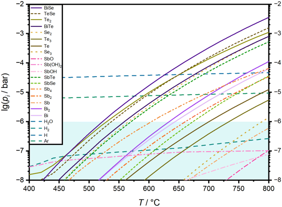 | ||
| Fig. 1 Simulated temperature dependent equilibrium partial pressures above the solid BSTS with equimolar cation and anion ratio. The blue area highlights partial pressures that are too low to make a significant contribution to vapor transport. | ||
However, in reality and especially for BSTS with compositions that deviate from this stoichiometry, the occurring transport reactions are more complex and involve the other vapor species with high vapor pressures like Se2 or Te2, whereas the individual equilibrium partial pressures depend on the initial composition of the BSTS. The thermodynamic simulations provide insights into the appropriate parameters for a rational and successful synthesis of BSTS nanocrystal growth during CVT experiments.
3.2. BSTS bulk materials investigation
To investigate the elemental composition of the prepared starting materials, SEM and EDX were used. Fig. S3 in the ESI† shows the results of the EDX analysis performed on bulk BiSb(Te0.98Se0.02). The error bars presented are within the accepted values of the uncertainty of the EDX measurements. All measured samples confirm the existence of the elements Bi, Sb, Te, and Se in the samples, with an intensity ratio corresponding to the stoichiometric compounds BiSb(Te1−ySey)3(y = 0, 0.01, 0.02, …, 0.09).These starting materials serve as a source for our CVT experiments to grow BSTS nanocrystals. The XRD pattern were measured at room temperature for the BiSb(Te1−ySey)3(y = 0, 0.01, 0.02, …, 0.09) bulk starting materials in their powder form, as shown in the ESI† (Fig. S4). The observed Bragg reflexes correspond to BiSb(Te1−ySey)3 in a trigonal structure with the Rm space group. The absence of any additional reflections confirms the successful phase-pure synthesis for all prepared compositions. A slight shift of Bragg peaks toward higher angles, possibly expected for a solid solution, with an increasing content of selenium was clearly observed. This is due to the small differences of selenium amount (Δy = 0.01) between all the prepared compositions.
3.3. BSTS nanocrystal investigation
A scheme of a general CVT process of BSTS is illustrated in Fig. 2(a). The growth happens in a sealed quartz ampule placed in an oven with a defined temperature gradient. It proceeds as a decomposition–sublimation reaction of the source at temperature T1, followed by vapor transport to a lower temperature region and the condensation on a substrate at temperature T2. For a long-enough substrate, the local temperature gradient during the growth results in two zones with different densities of nanostructures (hot and cold zones), see Fig. 2(c). In general, the CVT-grown BiSb(Te1−ySey)3 nanocrystals were found predominantly in the form of an agglomerated crystalline material at the hot side of the substrate and as individual and spatially separated nanocrystals at the cold side of the substrate. | ||
| Fig. 2 Overview of CVT growth of BiSb(Te1−ySey)3 nanocrystals. (a) Schematics of the CVT setup and the synthesis process. The starting material and the substrate are placed inside two chambers of a silica ampoule. The deposition was enabled by a temperature gradient (see the text for details). (b) Layered crystal structure of BiSb(Te1−ySey)3. (c) The substrate is divided into two temperature zones (cold and hot). | ||
Importantly, it is possible to alter the morphology and the thickness of the grown nanocrystals by varying the growth conditions (Table S5 in the ESI†): (i) the temperature gradient, (ii) the source and substrate temperatures, (iii) the source–substrate distance, (iv) the growth duration, and (v) the substrate material. Other parameters, such as the amount of the starting material (∼1 mg), were fixed since we focus on the synthesis of nanocrystals for magneto transport-measurements. We obtained various morphologies of nanostructures deposited on the substrate such as nanoflakes (triangles, hexagons and rhombohedrons), nanoribbons, and nanowires, with nanometre heights from 20 to 40 nm and lateral sizes ranging from ∼0.5 to 20 μm, when particular parameters are changed while keeping other parameters constant.
(i) Nanocrystals with different thicknesses can be obtained by changing the temperature gradient (or the growth duration). Using a lower temperature gradient of ΔT = 80 K leads to the formation of thinner crystals with heights ranging from 20 to 40 nm (Fig. 3, sample S1), since the low temperature gradient limits the mass transport of the starting material to the deposition zone. Thus, the availability of materials at the substrate surface becomes limited, causing a slow growth rate as well as the formation of thinner crystals. Moreover, a lower temperature gradient can provide better nucleation control, with the reduction of material species flow rate. Nucleation sites may be more preciously determined, potentially resulting in flatter and thinner crystal growth. A high temperature gradient (ΔT = 170 K) can result in faster mass transport of the material species to the sink side and a higher density of nucleation sites, resulting in faster growth rates and the growth of thick crystals with visible facets (∼200 nm), see Fig. 3, sample S2.
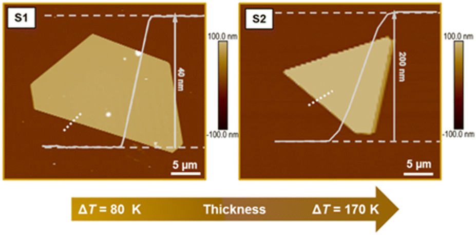 | ||
| Fig. 3 AFM images of BiSb(Te1−ySey)3 flakes show thickness dependence of the temperature gradient. S1, and S2 were grown at T1 = 500 °C, T2 = 420 °C, ΔT = 80 K and T1 = 500 °C, T2 = 330 °C, ΔT = 170 K, respectively. | ||
(ii) Based on thermodynamic simulations, three different temperature ranges were used to investigate the effect of the source and sink temperatures on crystal growth.
These are range R1 (T1 = 630 °C, T2 = 460 °C), range R2 (T1 = 560 °C, T2 = 390 °C), and range R3 (T1 = 500 °C, T2 = 330 °C), keeping the temperature gradient constant (ΔT = 170 K) in all cases. At higher temperature range R1 (Fig. 4, sample S5), larger regularly shaped crystals with a larger lateral size of ∼20 μm are formed, as compared to the size of the crystals grown at lower temperatures (R2 and R3) (Fig. 4, samples S4 and S3) with a length of ∼10 and 5 μm are obtained respectively. Some thin crystals were observed in all samples with a height of ∼20 nm. However, many thick agglomerated crystals extending up to a few micrometres in height were found at the hot side of the substrate. The higher temperature range promotes the formation of substantial quantity of viable nuclei and facilitated higher mass flow rates, thus resulting in a higher amount of material available for CVT growth. Consequently, the nuclei formed can be covered by subsequent particle depositions, eventually causing the nanocrystals to aggregate.
 | ||
| Fig. 4 Optical-microscope images of BiSb(Te1−ySey)3 flakes show size-dependence of the source temperature. S3, S4, and S5 were grown at T1 = 500 °C, T2 = 330 °C; T1 = 560 °C, T2 = 390 °C and T1 = 630 °C, T2 = 460 °C, respectively. | ||
(iii) Changing the distance between the source and substrate can have a significant impact on the morphology of the resulting nanostructures. When the substrate is placed as close as 8 cm to the source (Fig. 5, sample S6), the obtained crystals are irregularly shaped, sized and distributed mainly over the cold zone of the substrate. Increasing this distance to 12 and further 16 cm results in the formation of more regularly shaped crystals and a decrease in size, while also nanowires grow on the colder side of the substrate (for 16 cm). The change in crystal morphology can be explained by the decrease of the mass transport rate with increasing transport distance, as CVT is a diffusion-based process. While for 8 cm distance, the growth process of the nanocrystals is too fast to form distinctly shaped crystals, the larger distances and thus a slower growth process enables the formation of the energetically more favorable regularly shaped nanocrystals. Furthermore, longer distances between source and sink also increase the number of formed nuclei, whereas also differences appear between the colder and the hotter sides of the substrates. These might be a result of the slower diffusion process and a potential local difference in the build-up of the initial supersaturation before the nucleation. Furthermore, we can observe an increase in the number of the formed nuclei on the substrate with increasing the distance. This is also inconsistent with the fact that for shorter distances, the temperature at the hot zone of the substrate is still high enough to re-evaporate recently formed nuclei and form larger crystals in the cold zone, which is energetically more favourable. So, we see for short distances mainly nuclei and crystals at the cold zone of the substrate whereas for long distances nuclei and crystals can be observed on the entire substrate.
 | ||
| Fig. 5 Optical-microscope images of BiSb(Te1−ySey)3 flakes show a morphology dependence of the ampoule length. The distance between the source and the sink is 8 cm for S6 and 16 cm for S7. | ||
(iv) Long duration growth results in an increase of the size in all directions (X, Y, Z) and the number of deposited crystals. At short reaction time (4 h), there is no significant crystal growth on the substrate (Fig. 6, sample S8). Only very few crystals with predominant nanowire morphology can be observed. At a long growth duration (36 h) (Fig. 6, sample S11), many crystals are grown on the substrate. A longer growth time can promote the continuous expansion of more nuclei into different growth directions, rather than being limited to one specific direction. It is important to note that the influence of reaction time on crystal growth varies by changing the temperature. For example, a larger crystal size can be obtained during a short reaction time (4 h) when a high source temperature is applied (T1 = 630 °C) (Fig. 4, sample S5).
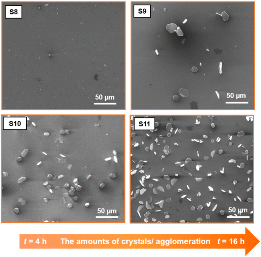 | ||
| Fig. 6 SEM images of BiSb(Te1−ySey)3 flakes show agglomeration-dependence of the duration growth. S8, S9, S10, and S11 were grown for 4 h, 8 h, 12 h, and 16 h, respectively. | ||
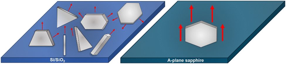
(v) Besides Si/SiO2, other substrates, such as A-plane sapphire (110), Si, and BaF2 were also used to grow BSTS crystals (Fig. 7, sample S12–S14). The ability to grow on various amorphous or crystalline substrates allow for exploration of the interaction between the BSTS-substrate and associated properties for diverse applications. Nanocrystals with different morphologies and orientations can be obtained. For example, nanocrystals on an A-plane sapphire substrate preferably grow perpendicular to the substrate surface, while nanocrystals on Si/SiO2 did not show preferential growth and were deposited randomly. In general, the growth direction of nanocrystals was mainly determined based on the crystallographic orientation of the substrate. However, other factors such as varying surface energy of the substrate material, and growth conditions may influence the growth direction. Since the relevant (growth) surface of the Si/SiO2 substrate is amorphous, it cannot imply any epitaxial effects and the crystals grow in random orientations on the substrate surface. In contrast to this, the crystalline surface of the A-plane sapphire enables epitaxial effects for the growth. However, in this case a potential strong mismatch of the atomic positions of the 2D BSTS layer and the surface of the sapphire substrate seems to affect the crystal growth process by promoting an out-of-plane growth of the BSTS in order to minimize the epitaxial mismatch. The different growth processes of BiSb(Te1−ySey)3 nanocrystals deposited on Si/SiO2 and sapphire are schematically depicted in Fig. 8. See more figures in the ESI.†
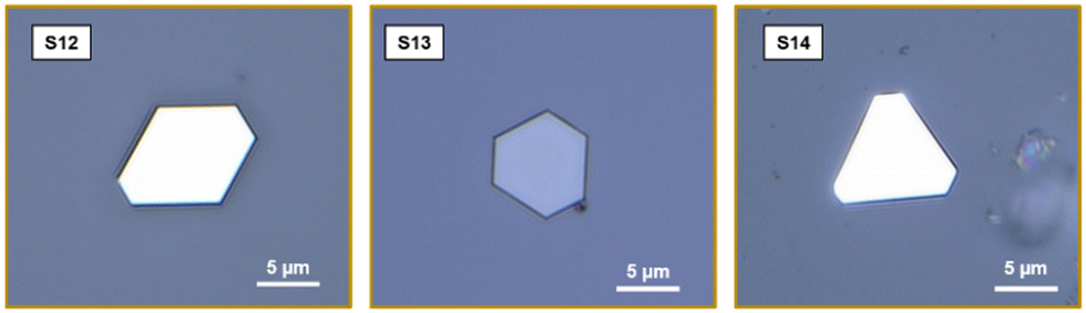 | ||
| Fig. 7 Optical-microscope images of BiSb(Te1−ySey)3 flakes grown on different substrates, S12, S13, and S14 were deposited on Al2O3, Si, and BaF2 respectively. | ||
 | ||
| Fig. 8 A growth process sketch of BiSb(Te1−ySey)3 nanocrystals grown in different directions Si/SiO2, and A-plane sapphire substrates. | ||
SEM-EDX measurements indicate signals of bismuth, antimony, tellurium, and selenium. The expected elemental ratio could be confirmed. One example of this is shown in the ESI† (Fig. S10) for BiSb(Te0.99Se0.01)3. Due to overlapping of the relevant Sb and Te peaks in the EDX, using the Bi content is the most reliable method of quantifying the results. An external standard calibration series was made to increase the precision of the SEM-EDX quantification results for grown crystals.
Thin nanostructures with thickness between 20 and 40 nm were found in all compositions (y = 0, 0.01, 0.02, …, 0.09). Crystals as thin as h = 20 nm, see Fig. S11 in the ESI,† were majority present in samples prepared at T1 = 500 °C, T2 = 420 °C, ΔT = 80 K. To quantify the reproducibility of optimal growth conditions, we determined the thickness of BiSb(Te1−ySey)3 crystals from multiple samples (Fig. 9). Nanoflakes are the most common morphology with heights mostly between 20 and 40 nm or higher than 80 nm. The thickness of nanowires and nanoribbons are found to be mostly between 60 and 80 nm or higher than 80 nm.
 | ||
| Fig. 9 Thicknesses of BiSb(Te1−ySey)3 nanostructures deposited via CVT. Several samples were considered for these statistics, samples prepared at T1 = 500 °C, T2 = 420 °C, ΔT = 80 K, t = 4 h. | ||
The local crystal structure of individual BSTS nanocrystals grown by CVT was confirmed using transmission electron microscopy. In particular, high-resolution transmission electron microscopy (HR-TEM) and selected-area electron diffraction (SAED) were performed. The results of BiSb(Te0.99Se0.01)3 nanocrystals are shown in Fig. 10(a–c). Fig. 10(a) shows a bright-field TEM image revealing the morphology of high crystal quality with partially faceted edges. The different grey levels of certain regions indicate different layers thicknesses, whereas the dark lines can be attributed to bending contours, which might be caused by the transfer process of the crystals from the substrate to the TEM grid. The HRTEM image in Fig. 10(b) depicts a highly periodic arrangement of atomic columns in BiSb(Te0.99Se0.01)3 with a determined lattice spacing of ∼2.17 Å for the {110} lattice plane fringes, which is slightly larger than the expected value from XRD for BiSbTe3 (2.165 Å). This slight difference may be attributed to the smaller ionic size of Se compared to Te. The good agreement between the experimental and the simulated SAED patterns along zone-axis orientation [001] for BiSb(Te0.99Se0.01)3 nanocrystals (Fig. 10(c)) confirms the high quality of the crystals. Consequently, HR-TEM and SAED investigations verify the hexagonal symmetry of the synthesized BiSb(Te0.99Se0.01)3 that can be assigned to the space group Rm.
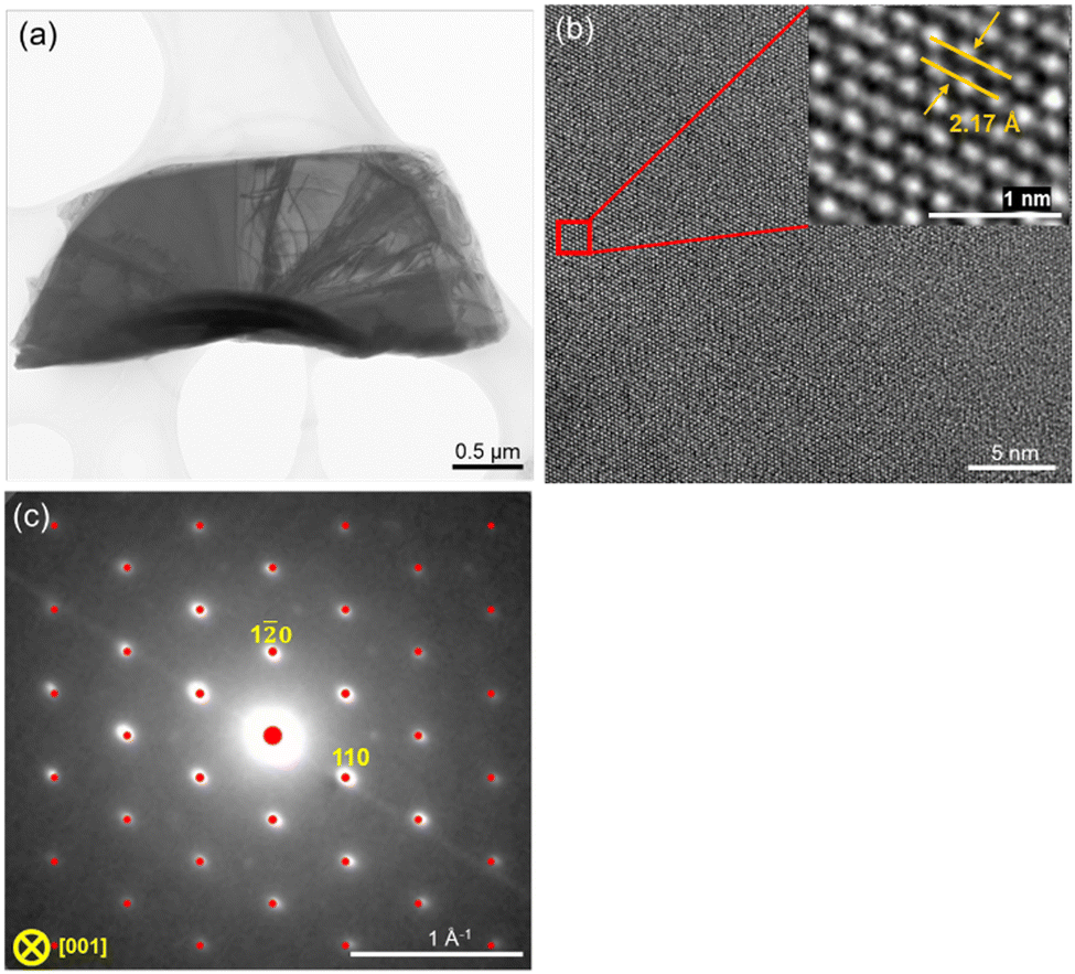 | ||
| Fig. 10 TEM and SAED images of BiSb(Te0.99Se0.01)3. (a) Bright-field TEM image of a representative nanoflake on lacey carbon. (b) High-resolution TEM image showing the atomic arrangement of the atoms along the [001] zone axis in which the top right image (b) represents the zoom-in of the area marked by a red square (c) SAED pattern of the nanoflake (a) oriented along [001] zone axis (white) overlapped with a corresponding simulated pattern (red). | ||
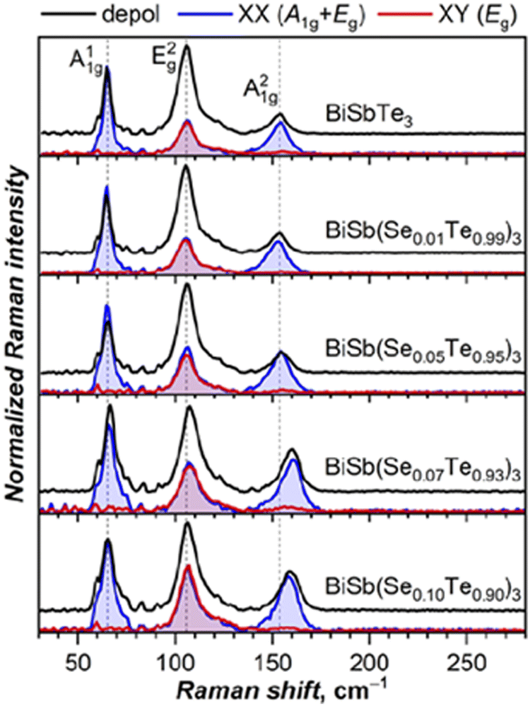
Raman spectra of BiSb(Te1−ySey)3 (y = 0, 0.01, 0.05, 0.07, 0.10) nanocrystals were studied to understand the effect of substitution on Raman-active modes and local symmetry. According to the XRD results, all these compounds are layered crystal assigned to the space group Rm, the same as in the parent compounds. The irreducible representation of the Raman active mode is described as Γvib = 2A1g + 2Eg. The lowest frequency Eg1 mode is usually very weak and can be rarely observed in experimental spectra,54 while three other modes are found at 63 (A11g), 103 (E2g), 134 (A21g) cm−1 in Bi2Te3 and at 69, 112, 165 cm−1 in Sb2Te3.55 In solid solutions with stochastic distribution of Bi/Sb and Te/Se atoms, the formal symmetry should be lower and can potentially lead to a splitting of the peaks. However, experimental spectra of all studied BiSb(Te1−ySey)3 compositions still show three Raman peaks, although somewhat broadened (Fig. 11). Note that earlier Raman studies of three-component solutions also showed three peaks for most of the compositions.56–58 Polarized measurements were then performed to evaluate if Eg and A1g modes partially mix in BiSb(Te1−ySey)3. A1g modes should be active only in parallel (XX) configuration, while Eg modes are active in both parallel and cross-polarized (XY) geometries. The measurements revealed that the A11g mode strictly follows the expected polarization pattern, but the A21g mode shows residual intensity in the XY polarization geometry. Besides, E2g and A21g peaks develop an asymmetry with tails towards each other. Thus, we conclude that effective Rm symmetry is still operative for vibrational modes, but signatures of the mode mixing are also evident.
 | ||
| Fig. 11 Raman spectra of different compositions of BiSb (Te1−ySey)3 nanocrystals measured at the excitation wavelength of 660 nm. For each composition, depolarized spectrum (black) is compared to the spectra measured in parallel (XX, blue) and cross-polarized (XY, red) geometries. | ||
Peak positions of A11g, E2g, and A21g modes in BiSbTe3 at 65, 106, and 154 cm−1 are intermediate between those in Bi2Te3 and Sb2Te3. Substitution of Te by Se should induce a positive frequency shift, because Se atoms are lighter, smaller in size and stronger in electronegativity compared to Te, which leads to shortening of the chemical bonds between Se and Bi. In the experimental spectra, the shifts are hardly detectable up to the composition of y = 0.05, but become more apparent for a higher content of Se (Fig. 11). Upon increasing y to 0.10, the most pronounced shift of ∼5 cm−1 is observed for the A21g mode, E2g frequency increases by 1–2 cm−1, while A11g remains unchanged.
3.4. Magneto-transport measurements
Magneto-transport measurements were performed on individual nanostructures connected with Ti/Au contacts patterned in a Hall-bar geometry, down to about 2 K and applying a magnetic field up to 18 T, perpendicular to the sample plane. The transport properties of 25 nm-thin nanostructures were investigated in detail for two different compositions (y = 0.01 and 0.05) and compared to previous measurements made on a ternary BiSbTe3 nanostructure.21 Here we focus on three devices (Fig. 12), each one showing the typical behaviour observed for a given composition. First, the temperature dependence of the longitudinal resistance shows either a metal-like behaviour or a crossover from semiconducting to metal-like properties, depending on the relative contributions of the bulk and surface states. As shown in Fig. 13, the resistance ratio R(T)/R (280 K), independent of geometric factors reveals the increased mobility in nanostructures with a low selenium content, giving a rather large residual resistance ratio R(280 K)/R(2 K). Given that the bulk density is reduced for these compounds, the metallic behaviour is dominated by surface-state transport, as confirmed by the large magneto-resistance measured at 2 K (Fig. 14) and the onset of Shubnikov-deHaas oscillations above 5 T. both revealing the enhanced mobility of charge carriers. On the contrary, nanostructures with a higher selenium content (y = 0.05) have a larger bulk contribution to the total conductance, with a non-degenerate semiconductor behaviour, and a reduced average mobility. The reduction of the bulk-carrier density for BSTS nanostructures with a low Se content is directly evidenced from Hall measurements (Fig. 15), revealing the transition from p-type (for y = 0) to n-type transport (for y = 0.01), as well as a non-linear behaviour typical for multi-band transport and some plateaus in the transverse resistance due to the formation of Landau level in samples with enhanced mobilities. Small variations were found between different flakes with the same nominal composition (grown on the same substrate), as expected from their different thicknesses and partial bulk-carrier depletion at interfaces due to band bending. For thicker nanostructures, small variations were found between different flakes with the same nominal composition (grown on the same substrate), due to the thickness dependence of the bulk contribution to the conductivity and/or to the bulk-carrier partial charge transfer to the interfaces (modified surface-state conductivity).31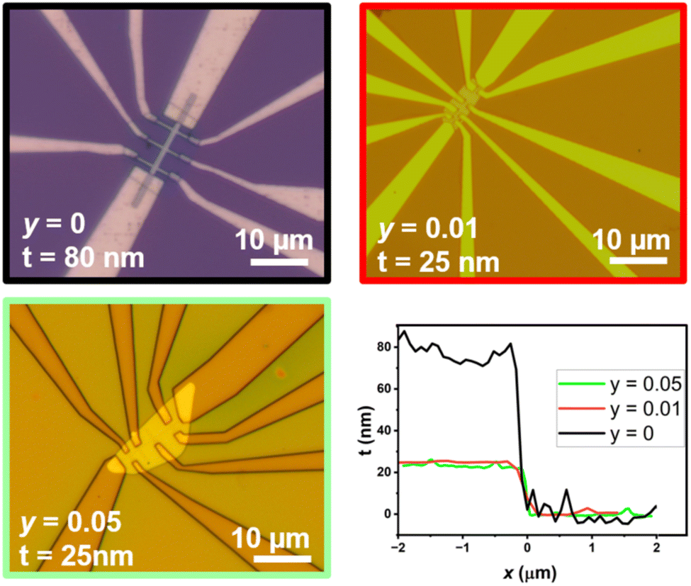 | ||
| Fig. 12 Optical-microscope images of the three electrically connected thin BiSb(Te1−ySey)3 flakes and their respective AFM thickness profiles. Coloured frames of the images are corresponding to the respective plot colours. | ||
 | ||
| Fig. 13 Temperature dependence of the resistance, normalized to the value measured at 280 K, for three different compositions (y = 0, 0.01 and 0.05). | ||
 | ||
| Fig. 14 Longitudinal magneto-resistance, measured at 2 K, for three different compositions (y = 0, 0.01 and 0.05), showing the enhanced mobility for a small Se content (onset of Shubnikov-deHaas oscillations around 5 T). | ||
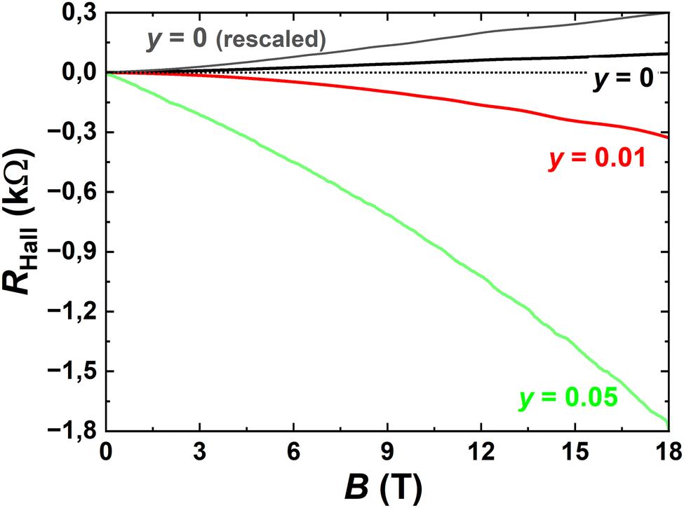 | ||
| Fig. 15 Transverse magneto-resistance, measured at 2 K, for three different compositions (y = 0, 0.01 and 0.05), showing the evolution from p-type to n-type charge transport. For comparison, the data obtained for y = 0.00 (80 nm) are also shown rescaled to an equivalent thickness of 25 nm. | ||
4. Conclusions
We successfully synthesized thin nanocrystals of BiSb(Te1−ySey)3 (y = 0, 0.01, 0.02, …, 0.09) using a transport agent-free CVT method and taking thermodynamic calculations into consideration. The structural and chemical compositions of the bulk starting materials were studied by powder X-ray diffraction and EDX, confirming a phase pure synthesis for all prepared compositions. The careful control of the synthesis conditions (source and substrate temperatures, temperature gradient, source–substrate distance, growth duration, and substrate material) allowed us to determine the optimal conditions for growing high-quality thin nanostructures. These have a smooth surface with well-faceted edges and metallic reflection, different morphologies (nanowires, nanoribbons, and planar triangular or hexagonal flakes) and a thickness of 20–40 nm with a lateral size range from ∼0.5 μm to ∼20 μm. Nanocrystals deposited on Si/SiO2, A-plane sapphire, Si, and BaF2 substrates demonstrated different growth directions.HRTEM/SAED and EDX data confirmed the high quality of the grown nanocrystals and the Rm trigonal crystal lattice structure as well as the chemical compositions of BiSb(Te1−ySey)3 with (y = 0, 0.01, 0.02, …, 0.09). A systematic Raman spectroscopy study performed on different compositions of BiSb(Te1−ySey)3, indicated that the vibrational modes are shifted to higher frequency for an increased incorporation of Se towards the substituting Te sites. Magneto-transport measurements revealed a large bulk-charge compensation in these quaternary-compound nanostructures, with dominant topological surface-state transport in thin nanoflakes, associated with a higher mobility of charge carriers.
Author contributions
N. A. and S. H. conceived and designed the project. N. A. conducted the synthesis of materials and analysis, and optical, SEM, EDX, AFM and pXRD characterization. S. F. completed the thermodynamic modelling. D. W. performed the HR-TEM measurements. A. P. and S. S. executed the RAMAN measurements. T. C., R. G. and J. D. carried out magneto-transport measurements and analysis. The manuscript was written by N. A. based on contribution from all authors. S. H., B. B. and M. M. supervised the work.Data availability
The data supporting this article have been included as part of the ESI.†Conflicts of interest
There are no conflicts to declare.Acknowledgements
The authors are grateful to Sandra Nestler for the cutting substrates, Robert Heider and Katrin Wruck for excellent lab assistance. N. A. acknowledges financial support from Palestine Technical University – Kadoorie, Palestine. N. A. and M. M. acknowledge financial support from the Deutsche Forschungsgemeinschaft (DFG; RTG 2767, Project ID No. 2946447). D. W. acknowledges funding from DFG SFB 1415, Project ID No. 417590517. R. G., T. C. and J. D. acknowledge funding from the European Union's H2020 FET Proactive project TOCHA (No. 824140).References
- W. Tian, W. Yu, J. Shi and Y. Wang, The Property, preparation and application of topological insulators: a review, Materials, 2017, 10, 814 CrossRef PubMed.
- M. J. Gilbert, Topological electronics, Commun. Phys., 2021, 4, 70 CrossRef CAS.
- M. Jamali, J. S. Lee, J. S. Jeong, F. Mahfouzi, Y. Lv, Z. Zhao, B. K. Nikolic, K. A. Mkhoyan, N. Samarth and J.-P. Wang, Giant spin pumping and inverse spin hall effect in the presence of surface and bulk spin−orbit coupling of topological insulator Bi2Se3, Nano Lett., 2015, 15, 7126–7132 CrossRef CAS PubMed.
- K. Kondou, R. Yoshimi, A. Tsukazaki, Y. Fukuma, J. Matsuno, K. Takahashi, M. Kawasaki, Y. Tokura and Y. Otani, Fermi-level-dependent charge-to-spin current conversion by Dirac surface states of topological insulators, Nat. Phys., 2016, 12, 1027–1031 Search PubMed.
- S. D. Sarma, M. Freedman and C. Nayak, Majorana zero modes and topological quantum computation, npj Quantum Inf., 2015, 1, 1–13 Search PubMed.
- A. Y. Kitaev, Fault-tolerant quantum computation by anyons, Ann. Phys., 2003, 303, 2–30 CAS.
- M. Konig, S. Wiedmann, C. Brune, A. Roth, H. Buhmann, L. W. Molenkamp, X.-L. Qi and S.-C. Zhang, Quantum spin hall insulator state in HgTe quantum wells, Science, 2007, 318, 766–770 CrossRef PubMed.
- D. Hsieh, Y. Xia, D. Qian, L. Wray, J. Dil, F. Meier, J. Osterwalder, L. Patthey, J. Checkelsky and N. P. Ong, A tunable topological insulator in the spin helical Dirac transport regime, Nature, 2009, 460, 1101–1105 CrossRef CAS PubMed.
- C. L. Kane and E. J. Mele, Z2 Topological order and the quantum spin hall effect, Phys. Rev. Lett., 2005, 95, 146802 CrossRef CAS PubMed.
- L. Fu and C. L. Kane, Topological insulators with inversion symmetry, Phys. Rev. B: Condens. Matter Mater. Phys., 2007, 76, 045302 CrossRef.
- M. Franz, U-turns strictly prohibited, Nature, 2010, 466, 323–324 CrossRef CAS PubMed.
- D. Culcer, Transport in three-dimensional topological insulators: Theory and experiment, Phys. E, 2012, 44, 860–884 CrossRef.
- X.-L. Qi and S.-C. Zhang, Topological insulators and superconductors, Rev. Mod. Phys., 2011, 83, 1057 CrossRef CAS.
- W. Feng and Y. Yao, Three-dimensional topological insulators: A review on host materials, Sci. China: Phys., Mech. Astron., 2012, 55, 2199–2212 CrossRef.
- J. Dufouleur, L. Veyrat, B. Dassonneville, E. Xypakis, J. H. Bardarson, C. Nowka, S. Hampel, J. Schumann, B. Eichler and O. Schmidt, Weakly-coupled quasi-1D helical modes in disordered 3D topological insulator quantum wires, Sci. Rep., 2017, 7, 45276 CrossRef CAS PubMed.
- Y. Xia, D. Qian, D. Hsieh, L. Wray, A. Pal, H. Lin, A. Bansil, D. Grauer, Y. S. Hor, R. J. Cava and M. Z. Hasan, Observation of a large-gap topological-insulator class with a single Dirac cone on the surface, Nat. Phys., 2009, 5, 398–402 Search PubMed.
- Y. L. Chen, J. G. Analytis, J. H. Chu, Z. K. Liu, S. K. Mo, X. L. Qi, H. J. Zhang, D. H. Lu, X. Dai, Z. Fang, S. C. Zhang, I. R. Fisher, Z. Hussain and Z. X. Shen, Experimental Realization of a Three-Dimensional Topological Insulator, Bi2Te3, Science, 2009, 325, 178–181 CrossRef CAS PubMed.
- D. Hsieh, Y. Xia, D. Qian, L. Wray, F. Meier, J. H. Dil, J. Osterwalder, L. Patthey, A. V. Fedorov, H. Lin, A. Bansil, D. Grauer, Y. S. Hor, R. J. Cava and M. Z. Hasan, Observation of time-reversal-protected single-Dirac-cone topological-insulator states in Bi2Te3 and Sb2Te3, Phys. Rev. Lett., 2009, 103, 146401 CrossRef CAS PubMed.
- R. J. Cava, H. Ji, M. K. Fuccillo, Q. D. Gibson and Y. S. Hor, Crystal structure and chemistry of topological insulators, J. Mater. Chem. C, 2013, 1, 3176–3189 RSC.
- J. Zhang, C.-Z. Chang, Z. Zhang, J. Wen, X. Feng, K. Li, M. Liu, K. He, L. Wang and X. Chen, Band structure engineering in (Bi1−xSbx)2Te3 ternary topological insulators, Nat. Commun., 2011, 2, 574 CrossRef PubMed.
- F. Hansen, R. Fucke, T. Charvin, S. Froeschke, D. Wolf, R. Giraud, J. Dufouleur, N. Gräßler, B. Büchner and P. Schmidt, Direct deposition of (BixSb1–x)2Te3 Nanosheets on Si/SiO2 Substrates by Chemical Vapor Transport, Cryst. Growth Des., 2022, 22, 2354–2363 CrossRef CAS.
- D. Kong, Y. Chen, J. J. Cha, Q. Zhang, J. G. Analytis, K. Lai, Z. Liu, S. S. Hong, K. J. Koski and S.-K. Mo, Ambipolar field effect in the ternary topological insulator (BixSb1–x)2Te3 by composition tuning, Nat. Nanotechnol., 2011, 6, 705–709 CrossRef CAS PubMed.
- J. Kellner, M. Eschbach, J. Kampmeier, M. Lanius, E. Młyńczak, G. Mussler, B. Holländer, L. Plucinski, M. Liebmann and D. Grützmacher, Tuning the Dirac point to the Fermi level in the ternary topological insulator (Bi1−xSbx)2Te3, Appl. Phys. Lett., 2015, 107, 1–4 CrossRef.
- S. L. Benjamina, C. K. de Grootc, C. Gurnania, S. L. Hawkena, A. L. Hectora, R. Huangc, M. Jurae, W. Levasona, E. Reida, G. Reida, S. P. Richards and G. B. G. Stenning, Compositionally tunable ternary Bi2(Se1−xTex)3 and (Bi1−ySby)2Te3 thin films via low pressure chemical vapor deposition, J. Mater. Chem. C, 2018, 6, 7734–7739 RSC.
- K.-B. Han, S. K. Chong, A. O. Oliynyk, A. Nagaoka, S. Petryk, M. A. Scarpulla, V. V. Deshpande and T. D. Sparks, Enhancement in surface mobility and quantum transport of Bi2−xSbxTe3−ySey topological insulator by controlling the crystal growth conditions, Sci. Rep., 2018, 8, 17290 CrossRef PubMed.
- N. P. Stepina, D. V. Ishchenko, V. A. Golyashov, A. O. Bazhenov, E. S. Goldyreva, I. O. Akhundov, A. S. Tarasov, K. A. Kokh and O. E. Tereshchenko, Epitaxial Growth of the BiySb2–yTe3–xSex 3D topological insulator: physical vapor deposition and molecular beam epitaxy, Cryst. Growth Des., 2022, 22, 7255–7263 CrossRef CAS.
- J. Dufouleur, L. Veyrat, B. Dassonneville, C. Nowka, S. Hampel, P. Leksin, B. Eichler, O. G. Schmidt, B. Büchner and R. Giraud, Correction to enhanced mobility of spin-helical Dirac fermions in disordered 3D topological insulators, Nano Lett., 2016, 16, 6733–6737 CrossRef CAS PubMed.
- J. Dufouleur, L. Veyrat, B. Dassonneville, E. Xypakis, J. H. Bardarson, C. Nowka, S. Hampel, B. Eichler, O. G. Schmidt, B. Büchner and R. Giraud, Weakly-coupled quasi-1D helical modes in disordered 3D topological insulator quantum wires, Sci. Rep., 2017, 7, 45276 CrossRef CAS PubMed.
- F. De Juan, R. Ilan and J. H. Bardarson, Robust Transport Signatures of Topological Superconductivity in Topological Insulator Nanowires, Phys. Rev. Lett., 2014, 113, 107003 CrossRef PubMed.
- G. Siroki, P. D. Haynes, D. K. Lee and V. Giannini, Protection of surface states in topological nanoparticles, Phys. Rev, Materials, 2017, 1, 024201 Search PubMed.
- L. Veyrat, F. Iacovella, J. Dufouleur, C. Nowka, H. Funke, M. Yang, W. Escoffier, M. Goiran, B. Eichler and O. G. Schmidt, Band bending Inversion in Bi2Se3 Nanostructures, Nano Lett., 2015, 15, 7503–7507 CrossRef CAS PubMed.
- M. Brahlek, N. Koirala, N. Bansal and S. Oh, Transport properties of topological insulators: Band bending, bulk metal-to-insulator transition, and weak anti-localization, Solid State Commun., 2015, 215–216, 54–62 CrossRef CAS.
- Y. Ando, Topological insulator materials, J. Phys. Soc. Jpn., 2013, 82, 102001 CrossRef.
- L. A. Aslanov and S. F. Dunaev, Exfoliation of crystals, Russ. Chem. Rev., 2018, 87, 882 CrossRef CAS.
- H. Zhong, T. Mirkovic and G. D. Scholes, Comprehensive Nanoscience and Technology, Academic Press, 2010, 1st edn Search PubMed.
- E. Gao, S. Lin, Z. Qin, M. J. Buehler, X. Feng and Z. Xu, Mechanical exfoliation of two-dimensional materials, J. Mech. Phys. Solids, 2018, 115, 248–262 CrossRef CAS.
- Y. Huang, Y.-H. Pan, R. Yang, L.-H. Bao, L. Meng, H.-L. Luo, Y.-Q. Cai, G.-D. Liu, W.-J. Zhao and Z. Zhou, Universal mechanical exfoliation of large-area 2D crystals, Nat. Commun., 2020, 11, 2453 CrossRef CAS PubMed.
- X. Cao, C. Jiang, D. Tan, Q. Li, S. Bi and J. Song, Recent mechanical processing techniques of two-dimensional layered materials: a review, J. Sci.: Adv. Mater. Devices, 2021, 6, 135–152 Search PubMed.
- H. Xue, H. Yang, Y. Wu, G. Yao, D. Guan, S. Wang, H. Zheng, C. Liu, Y. Li and J. Jia, Molecular beam epitaxy of superconducting PdTe2 films on topological insulator Bi2Te3, Sci. China: Phys., Mech. Astron., 2019, 62, 1–5 CAS.
- J. Dong, L. Zhang, X. Dai and F. Ding, The epitaxy of 2D materials growth, Nat. Commun., 2020, 11, 5862 CrossRef CAS PubMed.
- A. Koma, Molecular beam epitaxial growth of organic thin films, Prog. Cryst. Growth Charact. Mater., 1995, 30, 129–152 CrossRef CAS.
- L. Sun, G. Yuan, L. Gao, J. Yang, M. Chhowalla, M. H. Gharahcheshmeh, K. K. Gleason, Y. S. Choi, B. H. Hong and Z. Liu, Chemical vapour deposition, Nat. Rev. Methods Primers, 2021, 1, 5 CrossRef CAS.
- B. Qin, H. Ma, M. Hossain, M. Zhong, Q. Xia, B. Li and X. Duan, Substrates in the synthesis of two-dimensional materials via chemical vapor deposition, Chem. Mater., 2020, 32, 10321–10347 CrossRef CAS.
- D. Kong, W. Dang, J. J. Cha, H. Li, S. Meister, H. Peng, Z. Liu and Y. Cui, Ambipolar Field Effect in Sb-Doped Bi2Se3 nanoplates by solvothermal synthesis, Nano Lett., 2010, 10, 2245–2250 CrossRef CAS PubMed.
- S. S. Hong, J. J. Cha, D. Kong and Y. Cui, Ultra-low carrier concentration and surface-dominant transport in antimony-doped Bi2Se3 topological insulator nanoribbons, Nat. Commun., 2012, 3, 757 CrossRef PubMed.
- Y. Yan, Z.-M. Liao, Y.-B. Zhou, H.-C. Wu, Y.-Q. Bie, J.-J. Chen, J. Meng, X.-S. Wu and D.-P. Yu, Synthesis and quantum transport properties of Bi2Se3 topological insulator nanostructures, Sci. Rep., 2013, 3, 1264 CrossRef PubMed.
- Y. Yan, L.-X. Wang, X. Ke, G. Van Tendeloo, X.-S. Wu, D.-P. Yu and Z.-M. Liao, High-mobility Bi2Se3 nanoplates manifesting quantum oscillations of surface states in the sidewalls, Sci. Rep., 2014, 4, 3817 CrossRef PubMed.
- M. Binnewies, R. Glaum, M. Schmidt and P. Schmidt, Chemical vapor transport reactions – a historical review, J. Inorg. Gen. Chem., 2013, 639, 219–229 CAS.
- M. Binnewies, R. Glaum, M. Schmidt and P. Schmidt, Chemical vapor transport reactions, Walter de Gruyter, 2012 Search PubMed.
- C. Nowka, L. Veyrat, S. Gorantla, U. Steiner, B. Eichler, O. G. Schmidt, H. Funke, J. Dufouleur, B. Büchner, R. Giraud and S. Hampel, Catalyst-free growth of single crystalline Bi2Se3 nanostructures for quantum transport studied, Cryst. Growth Des., 2015, 15(9), 4272–4278 CrossRef CAS.
- C. Nowka, Untersuchungen zu Gasphasentransporten in quasibinaren Systemen von Bi2Se3 mit Bi2Te3, Sb2Se3, MnSe und FeSe zur Erzeugung von Nanokristallen, Technische Universität Dresden, IFW-Dresden, Germany, 2016 Search PubMed.
- G. Krabbes, W. Bieger, K.-H. Sommer, T. Söhnel and U. Steiner, 2014 TRAGMIN 5.1 (available at: https://www.htw-dresden.de/luc/forschung/chemieingenieurwesen/festkoerperchemie/tragmin).
- C. W. Bale, E. Bélisle, P. Chartrand, S. Decterov, G. Eriksson, A. E. Gheribi, K. Hack, I.-H. Jung, Y.-B. Kang and J. Melançon, CALPHAD: Comput. Coupling Phase Diagrams Thermochem., 2016, 55, 1 CrossRef CAS.
- Y. Zhao, X. Luo, J. Zhang, J. Wu, X. Bai, M. Wang, J. Jia, H. Peng, Z. Liu and S. Y. Quek, Interlayer vibrational modes in few-quintuple-layer Bi2Te3 and Bi2Se3 two-dimensional crystals: Raman spectroscopy and first-principles studies, Phys. Rev. B: Condens. Matter Mater. Phys., 2014, 90, 245428 CrossRef.
- W. Richter and C. Becker, A Raman and far-infrared investigation of phonons in the rhombohedral V2–VI3 compounds Bi2Te3, Bi2Se3, Sb2Te3 and Bi2(Te1−xSex)3 (0 < x < 1), (Bi1−ySby)2Te3 (0 < y < 1), Phys. Status Solidi B, 1977, 84, 619–628 CrossRef CAS.
- V. Chis, I. Y. Sklyadneva, K. A. Kokh, V. Volodin, O. Tereshchenko and E. Chulkov, Vibrations in binary and ternary topological insulators: first-principles calculations and Raman spectroscopy measurements, Phys. Rev. B: Condens. Matter Mater. Phys., 2012, 86, 174304 CrossRef.
- C. Zhang, Z. Peng, Z. Li, L. Yu, K. A. Khor and Q. Xiong, controlled growth of bismuth antimony telluride BixSb2−xTe3 nanoplatelets and their bulk thermoelectric nanocomposites, Nano Energy, 2015, 15, 688–696 CrossRef CAS.
- R. R. Urkude and U. A. Palikundwar, Phonon dynamics of (Bi1−xSbx)2Te3 topological insulators by Raman spectroscopy, Phys. B, 2023, 655, 414754 CrossRef CAS.
Footnote |
| † Electronic supplementary information (ESI) available. See DOI: https://doi.org/10.1039/d4tc02508c |
| This journal is © The Royal Society of Chemistry 2024 |