
 Open Access Article
 This Open Access Article is licensed under a Creative Commons Attribution-Non Commercial 3.0 Unported Licence
Optical properties of Ga2O3 thin films grown by atomic layer deposition using GaI3 and O3 as precursors
Lauri
Aarik
 *,
Hugo
Mändar
,
Aarne
Kasikov
,
Aivar
Tarre
and
Jaan
Aarik
*,
Hugo
Mändar
,
Aarne
Kasikov
,
Aivar
Tarre
and
Jaan
Aarik
Institute of Physics, University of Tartu, W. Ostwaldi 1, 50411 Tartu, Estonia. E-mail: lauri.aarik@ut.ee
First published on 25th June 2024
Abstract
Properties of Ga2O3 thin films grown by atomic layer deposition from GaI3 and O3 on Si(100) and amorphous SiO2 substrates were investigated. The Ga2O3 films deposited on the bare Si and SiO2 substrates at 450–550 °C contained the κ-Ga2O3 phase while it was not possible to exclude the presence of the ε-Ga2O3 phase in these films, either. On the substrates coated with α-Cr2O3, α-Ga2O3 was obtained at 275–550 °C. The formation of crystalline phases caused a marked increase in the density, roughness, and in the growth rate as well. The refractive indices, determined for the κ/ε-Ga2O3 and α-Ga2O3 films with thicknesses over 70 nm, were 1.96 ± 0.03 and 2.01 ± 0.02, respectively. Corresponding values of amorphous films, deposited on Si at 150–425 °C, on SiO2 at 310 °C, and on α-Cr2O3/Si at 200–234 °C, were 1.86 ± 0.03 at 633 nm. The optical bandgap energies of amorphous Ga2O3, κ/ε-Ga2O3, and α-Ga2O3 were found to be 4.96, 5.22–5.28, and 5.28 eV in the approximation of direct optical transitions and 4.27, 4.43, and 5.09 eV, respectively, in the approximation of indirect optical transitions. The films of κ/ε-Ga2O3 and α-Ga2O3 served as effective antireflection coatings on the surface of silicon reducing the reflection down to 0.20% and 0.12%, respectively.
1. Introduction
Gallium oxide (Ga2O3) has attracted marked interest as a promising material for high-voltage electronic devices,1–3 high electron-mobility transistors,4 resistive switching memories,5,6 solar-blind radiation detectors,7–9 and scintillators.10 Gallium oxide has also been studied as a relatively hard material11,12 that can, therefore, be used in protective coatings. Furthermore, possibilities for application of Ga2O3 for surface passivation of silicon solar cells have been recently investigated.13 Owing to appropriate refractive index values and the relatively wide transparency gap of Ga2O3 extending from the infrared to the ultraviolet spectral range,13–18 Ga2O3 thin films can also be used in antireflective coatings of solar cells and photodetectors that are based on silicon and III–V materials. Additionally, Ga2O3 films could be applied as antireflective coatings of light-emitting diodes and diode lasers as well. In all these applications, high hardness is highly beneficial to ensure improved durability of the functional coatings.As shown previously, the optical properties of Ga2O3 thin films significantly depend on the crystal structure and phase composition formed in the deposition or post-deposition annealing process. Ga2O3 can be amorphous or form at least six crystalline phases: α-, β-, γ-, δ-, ε-, and κ-Ga2O3.19,20 A marked number of studies including the characterization of refractive index (n) and optical bandgap (Eg) have been conducted for amorphous films.13–18,20–26 The results obtained indicate that the optical properties of the amorphous films markedly depend on the deposition method13 as well as deposition process parameters.21 For instance, the bandgap values of 4.05–5.47 eV13–15,17,18,20,21,23–26 have been reported for amorphous Ga2O3 films from the (αhν)2versus hν plots, where α is the absorption coefficient and hν is the photon energy. The refractive index values reported for amorphous films range from 1.75 to 1.90 at 633 nm.13–18,21,22,24,25
In the list of crystalline phases, β-Ga2O3 with the monoclinic structure (space group C2/m) has attracted the most significant interest that is evidently related to the higher stability of this phase compared to the stabilities of other crystalline phases.19,20 Optical bandgap energies of 4.26–5.24 eV published for β-Ga2O314,16,24–31 are comparable to those of amorphous films while n values of 1.83–1.94 at 633 nm have been reported for β-Ga2O3.14,16,22,25,27,28,30
A marked number of publications have also been focused on optical properties of α-Ga2O3 (space group R![[3 with combining macron]](https://www.rsc.org/images/entities/char_0033_0304.gif) c) because this phase has high density and Eg values.19,20 For instance, the Eg values ranging from 5.04 to 5.36 eV have been determined from the (αhν)2versus hν curves recorded for α-Ga2O3 thin films in the vicinity of the absorption edge.20,26,32–35 A similar value (5.46 eV) for the lowest band-to-band transition energy was obtained for α-Ga2O3 from the analysis based on spectroscopic ellipsometry (SE) measurements and density functional theory calculations.36 The spectroscopic studies have also demonstrated that the absorption spectra of α-Ga2O3 have a more complex shape36–39 that has been interpreted assuming contribution of an exciton and two band-to-band transitions with bandgap energies of 5.58–5.62 and 6.18–6.44 eV, respectively.37–39
c) because this phase has high density and Eg values.19,20 For instance, the Eg values ranging from 5.04 to 5.36 eV have been determined from the (αhν)2versus hν curves recorded for α-Ga2O3 thin films in the vicinity of the absorption edge.20,26,32–35 A similar value (5.46 eV) for the lowest band-to-band transition energy was obtained for α-Ga2O3 from the analysis based on spectroscopic ellipsometry (SE) measurements and density functional theory calculations.36 The spectroscopic studies have also demonstrated that the absorption spectra of α-Ga2O3 have a more complex shape36–39 that has been interpreted assuming contribution of an exciton and two band-to-band transitions with bandgap energies of 5.58–5.62 and 6.18–6.44 eV, respectively.37–39
The α-Ga2O3 polymorph has also relatively high n values of 1.97–2.01 as can be determined from the real parts of dielectric constants determined from SE data.36,39 However, the information concerning this parameter and, particularly, its dependence on the deposition process parameters is still limited.
Hexagonal ε-Ga2O3 (space group P63mc) and orthorhombic κ-Ga2O3 (space group Pna21) are also known as polymorphs with relatively high density.19,40,41 According to theoretical calculations, the bandgap energies of ε-Ga2O3 and κ-Ga2O3 should be 4.27 and 4.62 eV, respectively.42 However, the experimental characterization of optical parameters of pure ε- and κ-Ga2O3 polymorphs is a complex task because it is difficult to reveal the presence or absence of ε-Ga2O3 in the thin films that contain κ-Ga2O3.40,41 Moreover, the unambiguous determination of the κ-Ga2O3 phase in thin films by the X-ray diffraction (XRD) method needs rather complex measurements.43,44 This is probably one reason for the limited number of papers reporting the Eg values of ε-Ga2O3 and κ-Ga2O3. In these publications, Eg values of 4.6–5 eV for ε-Ga2O345,46 and 4.9–5.14 eV for κ-Ga2O39,29,47,48 have been reported. Notably, even less information can be found for n of these polymorphs while the value of 1.6 reported for ε-Ga2O3 does not seem to be consistent with the relatively high density of this phase.19 Therefore, additional studies focused on the optical properties of ε-Ga2O3 and κ-Ga2O3 as well as α-Ga2O3 polymorphs are evidently needed.
The self-limiting nature of atomic layer deposition (ALD) enables synthesis of thin films controlling the thickness with sub-nanometre resolution,15–18,24,44 fabrication of conformal coatings on substrates with complex shapes,14,15,22 and deposition of films with uniform thicknesses on large-area substrates.18 However, the deposition of crystalline Ga2O3 films on substrates that do not support epitaxial growth has been a problem for the majority of ALD processes studied so far. In a recent study, thin films containing α-Ga2O3 as well as those containing κ-Ga2O3 were grown by ALD at sufficiently low growth temperatures (TG) using GaI3 and O3 as the precursors.44 Therefore, this precursor system opens new possibilities for deposition and investigation of crystalline Ga2O3 thin films. Moreover, the GaI3–O3 precursor combination ensured relatively high growth rates as well as very low concentrations of residual impurities in the films, deposited in a wide range of TG. For these reasons, the corresponding ALD process seems to be attractive for several applications, including technology of electronic devices, radiation detectors, waveguides, and optical coatings.
In electronics applications, the bandgap energy of a semiconductor dielectric material is a very important parameter, while in optical applications, bandgap energies as well as refractive indices and absorption coefficient values should be known. All these parameters depend on the phase composition of a material. However, impurities, structural defects, and surface roughness that are all related to the material synthesis method may also influence the performance of materials and thin films in various applications. Hence, proceeding from the earlier promising results,44 the application potential of the GaI3–O3 ALD process for the deposition of Ga2O3 thin films for optical applications was studied in the present work. For this purpose, films containing different Ga2O3 phases were deposited. The effect of substrates and ALD process parameters on the properties of the films was investigated. Significant effects of crystallization processes on the optical properties as well as growth rate were revealed. Application of Ga2O3 as a material of antireflection (AR) coatings was studied.
2. Experimental details
The Ga2O3 thin films were deposited on Si(100), amorphous SiO2, α-Cr2O3/Si(100), and α-Cr2O3/SiO2 substrates in a low-pressure flow-type ALD reactor described earlier.49 The α-Cr2O3 seed layers that were needed to grow α-Ga2O3 films were also deposited by ALD. The seed layer thicknesses (dSL) ranged from 0.7 to 9 nm. The ALD and post growth annealing processes employed to obtain α-Cr2O3 are described in a previous paper.50During ALD of Ga2O3, GaI3 (99%, Strem Chemicals, Inc.) used as a metal precursor was kept at a temperature of 130 °C to volatilize the precursor. The GaI3 vapour was transferred to the reaction zone with N2 (AS Linde Gas, 99.999%) that was used as a carrier and purge gas. O3 employed as an oxygen precursor was generated in a BMT Messtechnik 802N generator from O2 (AS Linde Gas, 99.999%). The O3 concentration, measured using a BMT Messtechnik 964 analyser at the output of the ozone generator, was set at 220–250 g m−3. An ALD cycle, repeated to obtain films with expected thicknesses (d), contained a GaI3 pulse, purge, O3 pulse, and another purge. Each of these reaction steps was 2 s in duration. For the deposition of Ga2O3 films studied in the present work, 500–2000 ALD cycles were used.
The elemental composition of the films was characterized using an X-ray fluorescence (XRF) spectrometer ZSX-400 (Rigaku Corp.). The phase composition, texture, density, and surface roughness were determined using an X-ray diffractometer Smartlab (Rigaku Corp.) with CuKα radiation generated at a tube power of 8.1 kW. Grazing incidence X-ray diffraction (GIXRD) carried out at an incidence angle ω = 0.5°, coplanar θ–2θ-XRD and non-coplanar XRD were applied for phase composition and texture studies, while the X-ray reflection (XRR) method was used for the thickness, density, and surface roughness characterization. Crystalline phases observed in the films were identified on the basis of powder diffraction database ICDD PDF-2 (version 2023) and/or single crystal database ICSD (version 2022).
Optical properties were investigated using a spectroscopic ellipsometer GES-5E (Semilab, Inc.) and spectrophotometer V-570 (Jasco, Inc.). The n values were determined from the SE data as well as from the spectral oscillations of optical transmission spectra.51 To analyse the SE data for the Ga2O3 films deposited on Si and SiO2 substrates, one-layer fitting was used. In the case of films deposited on the α-Cr2O3 seed layers, an additional layer was added to the model that the fitting was based on. The thickness of this layer was calculated together with that of the Ga2O3 film. The absorption spectra were calculated from the transmission and reflection spectra52 measured at normal incidence in a wavelength (λ) range of 190–800 nm.
3. Results and discussion
3.1. Phase composition
Consistent with the results of earlier studies,44 the X-ray diffractograms depicted in Fig. 1(a) and (b) demonstrate that the films deposited on Si at TG ≥ 425 °C and on α-Cr2O3/Si at TG ≥ 275 °C contained crystalline phases, while the films deposited at lower TG were amorphous. The crystalline phases, identified on the basis of diffractograms presented in Fig. 1(a) and (b), were ε-Ga2O3 and/or κ-Ga2O3 on bare Si substrates and α-Ga2O3 on α-Cr2O3/Si. The same phases were obtained on bare SiO2 and α-Cr2O3/SiO2 substrates, respectively (Fig. 1(c) and (d)). Regardless of the film thickness, which varied from 74 to 210 nm, and TG, which varied from 450 to 550 °C, the highly developed preferential (0 0 1) orientation of ε-Ga2O3 and/or κ-Ga2O3 was formed in the films deposited on Si (Fig. 1(a)) as well as on SiO2 (Fig. 1(c)). | ||
| Fig. 1 Coplanar θ–2θ-XRD diffractograms of (a), (b) 74–97 nm thick Ga2O3 films grown on (a) bare Si and (b) α-Cr2O3/Si substrates, and (c), (d) 185–319 nm thick Ga2O3 films grown on (c) SiO2 and (d) α-Cr2O3/SiO2 and α-Cr2O3/Si substrates. Growth temperatures and film thicknesses are shown at corresponding diffractograms. (b) The α-Cr2O3 seed layer thicknesses (dSL) were 9 ± 3 nm. Miller indices of α-Ga2O3 (α) and κ-Ga2O3 (κ) are added to corresponding XRD reflections. Reflections attributable to the substrates and/or sample stage of diffractometer are marked with asterisks. | ||
On α-Cr2O3/Si and α-Cr2O3/SiO2 substrates, the (0 0 1) orientation of α-Ga2O3 was the prevalent one, especially in the thinner films grown at lower temperatures (Fig. 1(b)). This conclusion is based on the result that the reflection 0 0 6, which has an intensity of 3% relative to the 1 0 4 reflection of an ideal polycrystalline material (PDF-2 file 01-074-1610), is the most intense one in the diffractograms of the films grown at 275–350 °C (Fig. 1(b)). However, with increasing TG and film thickness, the relative intensity of the 0 0 6 reflection decreased (Fig. 1(b) and (d)) and approached the corresponding value of a powder material.
As the reflections of ε-Ga2O3 overlap with those of κ-Ga2O3,40,41,43,44 it is not possible to conclude on the basis of the coplanar θ–2θ XRD diffractograms presented in Fig. 1(a) and (c), which of these two phases was formed on bare Si and SiO2 substrates. However, there are a few κ-Ga2O3 reflections, for instance reflections 0 1 3 and 1 2 2, that do not have counterparts in the diffractogram of ε-Ga2O3.40,43,44 Unfortunately, in the case of κ-Ga2O3 films with highly developed (0 0 1) preferential orientation of crystallites, these reflections cannot be recorded by XRD using the coplanar θ–2θ geometry. Therefore, non-coplanar XRD analysis was performed to obtain more information about the phase composition of the films grown on bare Si and SiO2. In this analysis, the sample inclination angle (χ) was varied, while the θ–2θ XRD diffractograms for selected 2θ ranges were recorded (Fig. 2).
 | ||
| Fig. 2 Selected XRD reflections recorded in non-coplanar θ–2θ geometry at different inclination angles χ for a 210 nm thick Ga2O3 film grown on bare Si (solid lines) and 180 nm thick Ga2O3 film grown on bare SiO2 (dotted lines). The films were grown at 450 °C. | ||
According to the results of this analysis, the reflection observed in the coplanar diffractograms at around 30.5° (Fig. 1(a) and (c)) peaked at χ = 20.5° in the diffractogram of the film grown on Si and at χ = 20.2° in the diffractogram of the film grown on SiO2 (Fig. 2). The 2θ value of 30.7°, refined from the non-coplanar analysis, matched with the 0 1 3 reflection position of κ-Ga2O3. As β-Ga2O3 could also contribute to the reflection at these 2θ values, a χ scan was also recorded at 48.7° where the 5 1 0 reflection of β-Ga2O3 with a relative intensity of 20% was expected to appear (ICSD coll. code 83645) provided that this phase was present in the films. However, the χ scan did not reveal this reflection. Thus, there were no detectable amounts of β-Ga2O3 in these films. Consequently, the reflection observed at 30.7° belonged to κ-Ga2O3. Additionally, a reflection attributable only to (1 2 2) atomic planes of κ-Ga2O3 appeared at 2θ = 33.3° and χ values of 56.2° and 55.7° in the diffractograms of films grown on bare Si and SiO2, respectively (Fig. 2). Within a precision of 1.0–1.6°, these χ values observed were equal to the angle between the (1 2 2) and (0 0 1) planes of κ-Ga2O3 (54.6°). Hence, the appearance of the (1 2 2) reflection in non-coplanar and (0 0 l) reflections in coplanar analysis confirmed the presence of κ-Ga2O3 in these films. Unfortunately, the XRD analysis did not allow us to exclude the presence of ε-Ga2O3 in the films deposited on bare Si and SiO2. Therefore, the phase of these films is denoted as κ/ε-Ga2O3 in the following sections of this paper.
The growth of κ/ε-Ga2O3 on substrates (such as Si and amorphous SiO2) that do not support epitaxial growth is one of the main advantages of the GaI3–O3 ALD process. In previous studies, the κ- and ε-Ga2O3 have mainly been observed in the films epitaxially grown on α-Al2O3 (0 0 1) (c-cut sapphire) substrates,7,9,20,25,31,41,45–48 whereas only in a few cases have the substrate temperatures below 500 °C been sufficient for formation of these phases.25,48 Moreover, a relatively complex method, that is, epitaxial lateral overgrowth, including the deposition of the TiO2 seed layer on c-sapphire and a following lithography process to form a pattern that supports the κ-Ga2O3 growth, has been developed53 and applied54 for improving the quality of κ/ε-Ga2O3 films. However, even in these cases, substrate temperatures of 540–570 °C have been used for deposition of the films by halide vapour phase epitaxy.53,54 Hence, the thermal ALD based on GaI3 and O3 provides a much simpler approach for deposition of films containing κ-Ga2O3.
Low concentration of impurities in the films deposited by ALD from GaI3 and O3 was probably a key factor that enabled growth of crystalline phases at relatively low temperatures. For instance, according to the results of XRF analysis, the iodine concentration did not exceed 0.01 at% in the 160–320-nm-thick films deposited on Si and SiO2 substrates at 450–500 °C. With decreasing TG, the iodine concentration increased reaching 0.05 at% at 310 °C and 1.5 at% at 200 °C.
3.2. Influence of crystallization on density, surface roughness, and growth rate
Expectedly, the densities as well as surface roughness values significantly depended on the formation of crystalline phases in the deposition process. The growth of α-Ga2O3 at TG ≥ 275 °C and κ/ε-Ga2O3 at TG ≥ 450 °C caused a marked increase in density (Fig. 3(a)) and roughness values (Fig. 3(b)) compared to the corresponding values of amorphous films.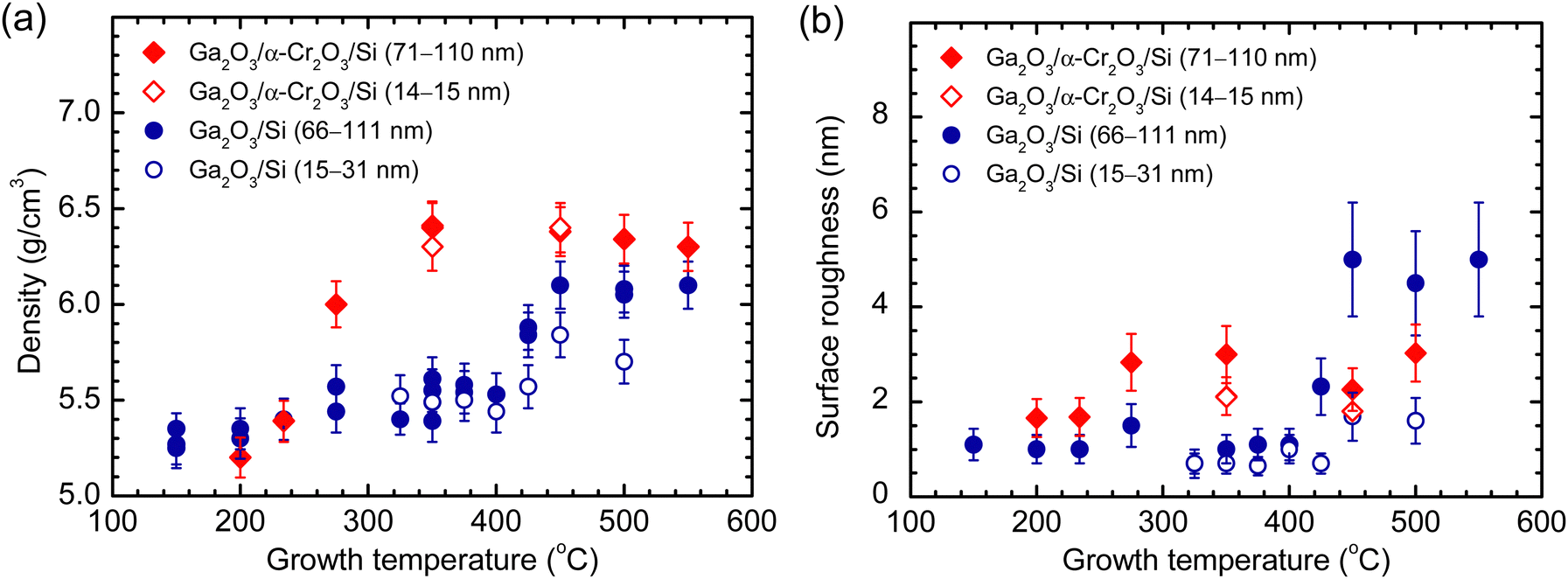 | ||
| Fig. 3 (a) Density and (b) surface roughness recorded by XRR as a function of growth temperature for 14–15 nm and 71–110 nm thick Ga2O3 films grown on α-Cr2O3/Si substrates, and for 15–31 nm and 66–111 nm thick Ga2O3 films grown on bare Si substrates. The thicknesses of α-Cr2O3 seed layers were 9 ± 3 nm. | ||
As can be seen in Fig. 3(a), the densities of X-ray-amorphous films did not depend on the film thickness and substrates, and showed only minor increase (from 5.25 ± 0.11 g cm−3 to 5.55 ± 0.16 g cm−3) with the TG increase from 150 to 400 °C. In contrast, the densities of films containing κ/ε-Ga2O3 formed on bare Si substrates at 450–550 °C were 5.93–6.10 g cm−3, while those of the α-Ga2O3 films obtained on the α-Cr2O3/Si substrates at 350–550 °C reached 6.40 g cm−3 (Fig. 3(a)). Notably, the densities recorded for the α-Ga2O3 and 66–111 nm thick κ/ε-Ga2O3 films were very close to the corresponding values calculated from the crystal structure parameters (6.11 g cm−3 for κ-Ga2O3 and 6.47 g cm−3 for α-Ga2O3), and reported in the XRD database (PDF-2 files 01-074-1610 and 01-082-3196) and earlier papers.40,41 Somewhat lower densities were determined for thinner (15–31 nm) films deposited on the bare Si substrates (Fig. 3(a)) at temperatures enabling growth of κ/ε-Ga2O3 (Fig. 1(a)). This result is in agreement with the results of earlier GIXRD studies44 and indicates that on bare Si substrates, the growth started with formation of amorphous or another low-density phase whereas the κ/ε-Ga2O3 phase gradually developed with increasing film thickness. In contrast, the densities close to the XRD database values of α-Ga2O3 were obtained even for 14–15 nm films deposited on α-Cr2O3/Si substrates at temperatures allowing crystallization of Ga2O3 on these substrates. Consequently, on these substrates, the growth of α-Ga2O3 started from the very beginning of deposition as it can also be concluded from the data of GIXRD studies described in our previous work.44
The growth of κ/ε-Ga2O3 caused more significant surface roughening than the growth of α-Ga2O3 did (Fig. 3(b)). The relatively small roughness increase related to the growth of α-Ga2O3 was evidently due to the uniform nucleation of this phase on α-Cr2O3. On the other hand, high roughness values and strong dependence of roughness on the film thickness, observed for the κ/ε-Ga2O3 films (Fig. 3(b)), were probably related to low concentration of nucleation centres on the bare Si substrates and faster growth of κ/ε-Ga2O3 compared to that of amorphous phase and different growth rates of crystallites with different orientations.
The results depicted in Fig. 4 confirm the conclusion about the faster growth of κ/ε-Ga2O3 compared to that of the amorphous phase. Fig. 4 clearly demonstrates that the growth per cycle (GPC) determined for films deposited with 600–700 ALD cycles markedly increased, when TG increased from 400 to 450 °C causing transition from the growth of amorphous phase to that of κ/ε-Ga2O3 (Fig. 1(a)). Interestingly, this kind of change in GPC was not observed in the case of markedly thinner films grown with 250 ALD cycles (Fig. 4). Considering the density (Fig. 3(a)) and surface roughness (Fig. 3(b)) values as well as the results of GIXRD studies reported earlier,44 it was possible to conclude that the crystal structure was less developed in the films grown on bare Si with 250 ALD cycles than that in the corresponding films grown with 600–700 ALD cycles.
 | ||
| Fig. 4 Growth per cycle as a function of growth temperature for Ga2O3 films grown with 250 and 600–700 ALD cycles on bare Si substrates and with 100 and 600–900 ALD cycles on α-Cr2O3/Si substrates. The thicknesses of α-Cr2O3 seed layers were 9 ± 3 nm. | ||
Notably, the TG increase from 275 to 350 °C, causing considerable improvement in crystallinity of the films deposited on α-Cr2O3 also led to increase in GPC (Fig. 4). Therefore, the GPC of α-Ga2O3 was also higher than that of amorphous Ga2O3. However, no effect of the film thickness on GPC was observed in this case. As can be seen in Fig. 4, the GPC values of films grown with 100 ALD cycles on α-Cr2O3 were very close to the GPC values of films grown with 600–900 cycles on these substrates. This result confirms the conclusion about uniform nucleation of α-Ga2O3 on α-Cr2O3 that is obviously related to epitaxial growth of α-Ga2O3 on α-Cr2O3.
In the TG ranges, where no transitions from amorphous to crystal growth were observed, the growth per cycle decreased with increasing TG. This kind of decrease in GPC can be caused by an increas in the I/Ga atomic ratio in the surface species formed during GaI3 adsorption. According to the results of a previous study,44 this ratio was as small as 0.7 at TG = 200 °C. Therefore, the possible I/Ga increase of up to 3 could lead to a marked increase in the steric hindrance of Ga adsorption and, correspondingly, to significantly smaller amount of Ga2O3 formed during an ALD cycle. A possible reason for the increase in the I/Ga ratio is the re-adsorption of gaseous I2, formed during the adsorption of GaI3. As discussed in an earlier publication,55 the re-adsorption of gaseous reaction products can explain the decrease in GPC as well as the thickness gradients that are similar to those observed in the case of films deposited from GaI3 and O3 at TG ≥ 450 °C.44 In contrast, at the precursor pulse durations used in our experiments, a considerable contribution of the thermal decomposition of GaI3 to the formation of thickness gradients was unlikely at temperatures of up to 500 °C because the precursor pulse duration increase from 2 to 5 s caused marked reduction in thickness gradients but no considerable increase in GPC in the substrate areas that were close to the outlet of the precursor supply line. Simulations of chemical reactions with the HSC Chemistry 7.0 software (Outotec Research Oy), indicating that significant thermal decomposition of GaI3 could start at temperatures exceeding 500–550 °C, confirmed this conclusion.
3.3. Optical properties
Absorption spectra of Ga2O3 films grown on SiO2 and α-Cr2O3/SiO2 substrates were calculated from transmission (Fig. 5(a)) and reflection (Fig. 5(b)) spectra. The transmission spectra (Fig. 5(a)) as well as the absorption spectra (Fig. 6(a)) demonstrate that the films were transparent or weakly absorbing at the wavelengths down to 290 nm and hν values of up to 4.3 eV, approximately. The decrease in the intensities of transmission maxima observed with decreasing wavelength in this range was evidently related to the contribution of light scattering caused by the surface roughness and material inhomogeneities. According to XRR analysis, the surface roughness values of these films exceeded 5–6 nm. This kind of roughness was estimated to be sufficient to explain the transmission decrease observed at wavelengths down to 290–300 nm. This decrease in the transmission resulted in the modest increase in the absorption coefficient determined at hν values of up to 4.2–4.4 eV for films grown on bare SiO2 and of up to 4.9 eV for a film grown on the α-Cr2O3/SiO2 substrate (Fig. 6(a)).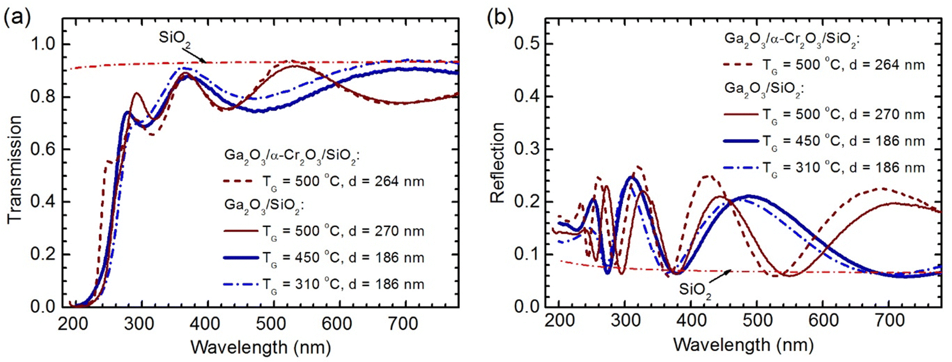 | ||
| Fig. 5 Optical (a) transmission and (b) reflection spectra of Ga2O3 films grown at different temperatures on SiO2 and α-Cr2O3/SiO2 substrates. The thickness of the α-Cr2O3 layer was 1.1 ± 0.4 nm. | ||
 | ||
| Fig. 6 (a) Absorption coefficient, (b) (αhν)2, and (c) (αhν)1/2 as a function of hν, and (d) refractive index as a function of wavelength determined for Ga2O3 films grown at different temperatures on SiO2 and α-Cr2O3/SiO2 substrates. The thickness of the α-Cr2O3 layer was 1.1 ± 0.4 nm. | ||
Expectedly, the absorption spectra depended on the phase composition of Ga2O3 (Fig. 6(a)). The absorption onset of amorphous films deposited on SiO2 at TG = 310 °C was observed at markedly lower hν values than those of κ/ε-Ga2O3 deposited on SiO2 at 450–500 °C and, particularly, that of α-Ga2O3 grown on α-Cr2O3/SiO2 at 500 °C (Fig. 6(a)). In the absorption spectrum of α-Ga2O3, two-step onset of absorption, causing a feature at 5.5–5.6 eV, was recorded (Fig. 6(a)). A similar feature, has been observed in earlier studies of α-Ga2O336–39 as well as monoclinic ZrO256 and HfO2.53,57 In all three cases, contribution of excitonic effects and specific electron band structures of these materials have been considered as possible reasons for this kind of feature.36–39,56,57 For instance, in the case of α-Ga2O3, an exciton band peaking at 5.5–5.6 eV and two different bandgap energies (5.61–5.62 and 6.18–6.52 eV) have been applied to fit the experimental curve recorded for the ordinary beam.38,39 Notably, the absorption onsets that appeared at around 5.1 and 5.8 eV in the absorption spectra of our α-Ga2O3 films coincided with those reported by Segura et al.,37 Kracht et al.38 and Feneberg et al.39 indicating that the bandgap energies of these films were very similar to each other.
However, in a number of applications, the performance of α at the optical absorption edge rather than in the range of strong absorption is of importance. Therefore, the Eg values are frequently determined from the (αhν)2versus hν or (αhν)1/2versus hν plots, while the former plots assuming direct optical transitions have mainly been used to determine optical bandgap energies of α-Ga2O3,20,26,32–35 ε-Ga2O3,45,46 κ-Ga2O3,9,47 and amorphous Ga2O3.13–15,17,18,20,21,23–26 Extrapolating the linear parts of the (αhν)2versus hν plots of our films (Fig. 5(b)) yielded the optical bandgap energies in the approximation of direct optical transitions (Edg) at 4.96 eV for amorphous Ga2O3, 5.22–5.28 eV for κ/ε-Ga2O3, and 5.28 eV for α-Ga2O3 (Table 1). The Edg values of amorphous Ga2O3 and α-Ga2O3 were consistent with corresponding values of 4.05–5.47 eV13–15,17,18,20,21,23–26 and 5.04–5.36 eV20,26,32–35 reported in earlier publications. In contrast, the Edg values determined for κ/ε-Ga2O3 exceeded those of 4.6–5 eV45,46 and 4.9–5.14 eV9,29,47,48 published for ε-Ga2O3 and κ-Ga2O3, respectively. It is also worth mentioning that Edg obtained for our amorphous Ga2O3 films were very close to the most typical values of 4.80–5.00 eV obtained for amorphous Ga2O3 films grown by ALD previously.13–16,18,24
| T G (°C) | Substrate | d (nm) | Phase | E dg (eV) | E ig (eV) |
|---|---|---|---|---|---|
| a The thickness of the α-Cr2O3 layer was 1.1 ± 0.4 nm. | |||||
| 310 | SiO2 | 188 | Amorphous | 4.96 ± 0.03 | 4.27 ± 0.03 |
| 450 | SiO2 | 185 | κ/ε-Ga2O3 | 5.28 ± 0.03 | 4.43 ± 0.03 |
| 500 | SiO2 | 270 | κ/ε-Ga2O3 | 5.22 ± 0.05 | 4.43 ± 0.04 |
| 500 | α-Cr2O3/SiO2a | 260 | α-Ga2O3 | 5.28 ± 0.03 | 5.09 ± 0.03 |
Comparing the absorption spectra (Fig. 6(a)) and Edg values obtained from the results depicted in Fig. 6(b), one can see that the absorption was relatively strong at the Edg values determined from the (αhν)2versus hν curves. Consequently, the direct transition analysis was not sensitive enough to the absorption at the photon energies close to the absorption edges of these materials. Furthermore, the linear parts in the (αhν)2versus hν plots of the films deposited on SiO2 at 450–500 °C were relatively short and appeared at photon energies significantly exceeding the Edg values determined from these plots (Fig. 6(b)). This obviously resulted in additional uncertainty in the determination of Edg for these films. Therefore, the optical bandgap energies were also determined from the (αhν)1/2versus hν plots (Fig. 6(c)) assuming indirect optical transitions between the valence and conduction bands. The Eig values obtained in this approximation were 4.27 eV for amorphous Ga2O3, 4.43 eV for κ/ε-Ga2O3, and 5.09 eV for α-Ga2O3 (Table 1). These energies correspond well to the absorption onsets (Fig. 6(a)). Therefore, it is possible that the Ga2O3 phases studied in this work have indirect bandgaps as it has been predicted for α-Ga2O3 in theoretical calculations.58–60 Notably, the Edg − Eig value of 0.19 eV, determined from the absorption spectra of α-Ga2O3 in this work is close to the corresponding values of 0.21–0.25 eV obtained from the first-principles calculations.58–60
Alternatively, there is a possibility that the bandgap is direct but the electron transitions do not follow the momentum selection rule, when the photon energies causing the transitions are close to the bandgap energies. The latter effect might be related to the structural defects, impurities, and/or band tails that can contribute to the electron transitions at photon energies close to the bandgap values.61 Therefore, it is not surprising that the recent experimental results of Ma et al.,62 yielding an Eig value of 5.02 eV for α-Ga2O3 from the (αhν)1/2versus hν plots, also indicate that contribution of indirect transitions to the shapes of absorption spectra at the absorption edge of this phase cannot be neglected.
Refractive indices determined as a function of wavelength for the Ga2O3 films deposited on SiO2 and α-Cr2O3/SiO2 substrates are depicted in Fig. 6(d). The experimental points with error bars correspond to the n values determined from the spectrophotometry data, while the curves were calculated from the results of SE measurements. Expectedly, the n values of κ/ε-Ga2O3 and α-Ga2O3 films grown on SiO2 and α-Cr2O3/SiO2 at 450 and 500 °C, respectively, were markedly higher than those of an amorphous film deposited on SiO2 at 310 °C (Fig. 6(d)). Very similar results, obtained for the 80–107 nm thick films on Si and α-Cr2O3/Si, are shown in Fig. 7.
 | ||
| Fig. 7 Refractive index as a function of wavelength determined by spectroscopic ellipsometry for Ga2O3 films grown at different temperatures on Si and α-Cr2O3/Si substrates. The thickness of the α-Cr2O3 layer was 1.1 ± 0.4 nm. | ||
The data presented in Fig. 7 demonstrate that the variation of TG from 200 to 375 °C and from 450 to 550 °C did not cause considerable changes in the n values and dispersion curves of the films grown on Si substrates. However, the TG increase from 375 to 450 °C causing the transition from the growth of amorphous phase to the growth of κ/ε-Ga2O3 led to a marked increase in n (Fig. 7). In line with the results presented in Fig. 6(d), even higher n values were measured for the α-Ga2O3 films deposited on the α-Cr2O3/Si substrates.
As it was expected, the films grown on Si and α-Cr2O3/Si substrates had n values that were very similar to those of the films deposited on SiO2 and α-Cr2O3/SiO2, respectively (Table 2). The minor differences observed did not exceed the experimental uncertainty. Comparing the results presented in Table 2 and Fig. 8, one can see that at d > 80 nm, the dependence of n on d was weak. However, at lower film thicknesses, n decreased with decreasing d (Fig. 8(a)).
| T G (°C) | Substrate | d (nm) | Phase | n at 365 nm | n at 633 nm |
|---|---|---|---|---|---|
| a The thickness of the α-Cr2O3 layer was 0.7 ± 0.3 nm. b The thickness of the α-Cr2O3 layer was 1.1 ± 0.4 nm. | |||||
| 310 | Si | 188 | Amorphous | 1.95 ± 0.02 | 1.86 ± 0.02 |
| 310 | SiO2 | 188 | Amorphous | 1.95 ± 0.02 | 1.86 ± 0.02 |
| 450 | Si | 189 | κ/ε-Ga2O3 | 2.01 ± 0.03 | 1.93 ± 0.02 |
| 450 | SiO2 | 185 | κ/ε-Ga2O3 | 2.02 ± 0.03 | 1.94 ± 0.02 |
| 500 | Si | 273 | κ/ε-Ga2O3 | 2.06 ± 0.03 | 1.98 ± 0.02 |
| 500 | SiO2 | 270 | κ/ε-Ga2O3 | 2.04 ± 0.03 | 1.98 ± 0.02 |
| 500 | α-Cr2O3/Sia | 269 | α-Ga2O3 | 2.06 ± 0.03 | 2.01 ± 0.03 |
| 500 | α-Cr2O3/SiO2b | 260 | α-Ga2O3 | 2.09 ± 0.03 | 2.02 ± 0.03 |
 | ||
| Fig. 8 Refractive index as a function of (a) thickness of films grown at 350, 450 and 500 °C and (b) growth temperatures of 82–107 nm thick films grown on Si and 79–101 nm thick films grown on α-Cr2O3/Si substrates. The α-Cr2O3 seed layer thicknesses were 9 ± 3 nm. The refractive indices were calculated at wavelengths of (a) 633 nm and (b) 365 and 633 nm from the spectroscopic ellipsometry data. | ||
As an one-layer model was used to analyse the SE data, one probable reason for the decrease in n observed with decreasing d at lower film thicknesses was the increasing contribution of surface roughness, causing the formation of surface layer with lower density and, correspondingly, a decrease in the mean value of n calculated from the SE results. For instance, the XRR analysis yielded surface roughness values of 0.9 and 1.0 nm for the 59 and 85 nm thick films grown on Si at 350 °C, 4.5 and 5.0 nm for the 44 and 85 nm thick films grown on Si at 450 °C, and 2.5 nm for the 43 and 83 nm thick films grown on α-Cr2O3/Si at 450 °C. Therefore, with the thickness decrease in these d ranges, the surface roughness decreased insignificantly or did not decrease at all. Correspondingly, the relative amount of material with lower n increased with decreasing film thickness leading to the decrease in the mean value of n.
To characterize the effect of TG on n in more detail, the values of n determined at wavelengths of 365 and 633 nm for films with thicknesses of 79–107 nm deposited on Si and α-Cr2O3/Si substrates are displayed in Fig. 8(b) as a function of TG. Comparison of the results presented in Fig. 1(a), (b) and 8(b) leads to a conclusion that the effect of TG on n is insignificant in the TG ranges where no phase transitions take place. For instance, no considerable influence of TG was observed on n of amorphous films grown on bare Si at 150–425 °C, κ/ε-Ga2O3 films grown on bare Si substrates at 450–550 °C, and α-Ga2O3 films grown on α-Cr2O3/Si at 350–550 °C. In contrast, marked increase in n of films deposited on bare Si and α-Cr2O3/Si is observed with the TG increase from 425 to 450 °C and from 230 to 350 °C, respectively (Fig. 8(b)), that is, with the transition from the growth of amorphous to that of crystalline films (Fig. 1(a) and (b)).
The n values, obtained for amorphous Ga2O3 in this work (Table 2 and Fig. 8(b)), were well comparable to the highest values (1.84–1.87 at λ = 633 nm) reported for amorphous films in previous ALD studies.13,14,16,18 In addition, the n values obtained for the films grown on α-Cr2O3/Si and α-Cr2O3/SiO2 in this work (Table 2 and Fig. 8(b)) were close to a value of 2.00 that can be determined from the ellipsometry data of Feneberg et al.39 published for the epitaxial films grown on α-Al2O3 (0 0 0 1) by ultrasonic mist chemical vapour epitaxy.
When comparing the results of our experiments with those of earlier studies, one can see that the n values of κ/ε-Ga2O3 films recorded at 633 nm (Table 2 and Fig. 8) are somewhat higher than the corresponding values of 1.83–1.94 at 633 nm reported for stoichiometric β-Ga2O3.14,16,22,25,27,28,30 One can also notice that refractive indices of 2.00–2.02 obtained for α-Ga2O3 at 633 nm in this work (Table 2 and Fig. 8) and by Feneberg et al.39 are close to that of 2.04 determined at 633 nm for γ-Ga2O3.58,63 However, the Edg and Eig values of α-Ga2O3 (Table 1) are markedly higher than the respective values of 5.0 and 4.4 eV58,63 reported for γ-Ga2O3.
In agreement with theoretical considerations and results obtained earlier for other materials,64–66 the refractive index values (Fig. 8) increase together with the material densities (Fig. 3(a)). Additionally, our data demonstrate that the Eg values are in positive correlation with the densities of Ga2O3 phases studied in this work. The latter result is not common for other materials. For instance, high-density rutile and TiO2-II phases of TiO2 have narrower bandgaps compared to that of the low-density anatase phase.66 An explanation for this difference can be deduced from the results of Ohta et al.,67 who investigated phase transition of anatase to TiO2-II at high hydrostatic pressures. They observed a predictable shift of the optical absorption edge of anatase to higher energies, caused by the reduction of average bond length and corresponding increase in the material density under the increasing hydrostatic pressure. However, at pressures causing the phase transformation from anatase to TiO2-II, an abrupt absorption-spectrum shift to lower energies appeared because of the atomic rearrangement. Therefore, the higher Eg values, recorded for Ga2O3 phases with higher densities in our experiments, indicate that the differences of the atomic arrangements in these phases from those in the Ga2O3 phases with lower densities do not cause bandgap shrinking that would be comparable to the Eg increase due to the decrease in the average bond length or unit cell volume.60,68
In the visible range of spectrum, the n2 values calculated on the basis of data depicted in Table 2 and Fig. 8 were close to the refractive index value of silicon.69 Therefore, the Ga2O3 films studied in this work were expected to be suitable for highly efficient single-layer antireflection (AR) coatings of silicon-based optoelectronic devices, for instance, solar cells and photodiodes. The reflection spectra, measured for silicon substrates coated with Ga2O3 and Ga2O3/α-Cr2O3 thin films at different temperatures, demonstrate that at wavelengths (λmin) corresponding to the reflection minima, the reflection values (Rmin) below 1% can be obtained for all coatings studied (Fig. 9 and Table 3). The lowest Rmin values that reached 0.12% were recorded for the α-Ga2O3/α-Cr2O3 AR coatings. However, the Rmin of the κ/ε-Ga2O3-coated Si was also very low (Table 3).
 | ||
| Fig. 9 Reflection spectra recorded in wavelength ranges of (a) 200–820 nm and (b) 400–820 nm for silicon substrates coated with Ga2O3 and Ga2O3/α-Cr2O3 antireflection coatings. (a) Reflection spectrum of bare silicon substrate is shown for comparison. The thickness of α-Cr2O3 was 1.5 ± 0.5 nm. | ||
| T G (°C) | Phase | Thickness (nm) | λ min (nm) | R min (%) |
|---|---|---|---|---|
| 200 | Amorphous | 73 ± 3 | 533 ± 5 | 0.75 ± 0.08 |
| 350 | Amorphous | 72 ± 3 | 540 ± 5 | 0.68 ± 0.07 |
| 450 | κ/ε-Ga2O3 | 70 ± 3 | 570 ± 5 | 0.20 ± 0.05 |
| 350 | α-Ga2O3/α-Cr2O3 | 68 ± 3/1.5 ± 0.5 | 570 ± 5 | 0.12 ± 0.04 |
It is also worth noting that the light transmission through the α-Ga2O3/α-Cr2O3 AR coatings is sufficiently high only at wavelengths exceeding 400 nm. At lower wavelengths, the absorption of light in the α-Cr2O3 seed layer might become significant. For instance, using the data published for α-Cr2O3 thin films,70 the absorption in a 1 nm thick seed layer was estimated to increase from ≤0.2% at 400 nm to 1.5% at 350 nm, 3.8% at 300 nm, and 8% at 200 nm. Hence at wavelengths below 400 nm, the κ/ε-Ga2O3-AR coatings are evidently more efficient than the α-Ga2O3/α-Cr2O3 AR coatings.
4. Conclusions
The results of this work confirm significant influence of the crystal growth and phase composition on the density and optical properties of Ga2O3. Notably the formation of phases with higher densities caused an increase in both the optical bandgap energies and refractive indices. The bandgap energies, estimated from the (αhν)2versus hν plots for the amorphous, κ/ε, and α phases of Ga2O3 with the densities of 5.2–5.6, 5.9–6.1, and 6.2–6.4 g cm−3, were 4.96, 5.22–5.28, and 5.28 eV, respectively. These values were consistent with previous data, obtained using the same approach that assumed domination of direct optical transitions in the absorption process. However, the bandgap values of 4.27, 4.43, and 5.09 eV, respectively, determined from the (αhν)1/2versus hν plots corresponding to the indirect transitions, characterized the optical absorption edge energies even better. This result indicates that most probably, the electron transitions, caused by absorption of radiation with photon energies close to the absorption edge, do not follow the momentum selection rule although most of the Ga2O3 phases have generally been considered to be direct bandgap materials. Influence of impurities and/or structural defects on optical transitions can be a possible reason for this effect. The refractive index values of amorphous Ga2O3, κ/ε-Ga2O3, and α-Ga2O3 films, measured at 633 nm for films with thicknesses exceeding 70 nm, were 1.86 ± 0.03, 1.96 ± 0.03 and 2.01 ± 0.02, respectively. Because of appropriate refractive index values, these Ga2O3 phases appeared to be suitable for applications in AR coatings allowing the reduction of reflection from the silicon surface down to 0.12–0.20%.The results of this work also reveal that the crystallization processes markedly influence GPC. Moreover, on the substrates that do not support epitaxial growth of a crystalline phase, the spontaneous crystallization may lead to considerable dependence of GPC on the Ga2O3 film thickness. These effects should also be considered when designing ALD processes for the deposition of optical coatings because, as a rule, the thickness is an important parameter of a thin film deposited for optical applications.
Data availability
Data are available upon request from the authors.Conflicts of interest
There are no conflicts to declare.Acknowledgements
The authors are grateful to Alma-Asta Kiisler and Peeter Ritslaid for technical assistance. The research was funded by the Estonian Research Council (grants PSG448 and PRG753).References
- S. J. Pearton, F. Ren, M. Tadjer and J. Kim, Perspective: Ga2O3 for ultra-high power rectifiers and MOSFETS, J. Appl. Phys., 2018, 124, 220901, DOI:10.1063/1.5062841.
- J.-S. Li, C.-C. Chiang, X. Xia, T. J. Yoo, F. Ren, H. Kim and S. J. Pearton, Demonstration of 4.7 kV breakdown voltage in NiO/β-Ga2O3 vertical rectifiers, Appl. Phys. Lett., 2022, 121, 042105, DOI:10.1063/5.0097564.
- A.-C. Liu, C.-H. Hsieh, C. Langpoklakpam, K. J. Singh, W.-C. Lee, Y.-K. Hsiao, R.-H. Horng, H.-C. Kuo and C.-C. Tu, State-of-the-art β-Ga2O3 field effect transistors for power electronics, ACS Omega, 2022, 7, 36070–36091, DOI:10.1021/acsomega.2c03345.
- J. Wang, H. Guo, C.-Z. Zhu, Q. Cai, G.-F. Yang, J.-J. Xue, D.-J. Chen, Y. Tong, B. Liu, H. Lu, R. Zhang and Y.-D. Zheng, ε-Ga2O3: a promising candidate for high-electron-mobility transistors, IEEE Electron Device Lett., 2020, 41, 1052–1055, DOI:10.1109/LED.2020.2995446.
- Z. Yang, J. Wu, P. Li, Y. Chen, Y. Yan, B. Zhu, C. S. Hwang, W. Mi, J. Zhao, K. Zhang and R. Guo, Resistive random access memory based on gallium oxide thin films for self-powered pressure sensor systems, Ceram. Int., 2020, 46, 21141–21148, DOI:10.1016/j.ceramint.2020.05.191.
- X. Li, J.-G. Yang, H.-P. Ma, Y.-H. Liu, Z.-G. Ji, W. Huang, X. Ou, D. W. Zhang and H.-L. Lu, Atomic layer deposition of Ga2O3/ZnO composite films for high-performance forming-free resistive switching memory, ACS Appl. Mater. Interfaces, 2020, 12, 30538–30547, DOI:10.1021/acsami.0c06476.
- M. Pavesi, F. Fabbri, F. Boschi, G. Piacentini, A. Baraldi, M. Bosi, E. Gombia, A. Parisini and R. Fornari, ε-Ga2O3 epilayers as a material for solar-blind UV photodetectors, Mater. Chem. Phys., 2018, 205, 502–507, DOI:10.1016/j.matchemphys.2017.11.023.
- H. Qian, X. Zhang, Y. Ma, L. Zhang, T. Chen, X. Wei, W. Tang, X. Zhou, B. Feng, Y. Fan, Y. Sun and B. Zhang, Quasi-vertical ε-Ga2O3 solar blind photodetectors grown on p-Si substrates with Al2O3 buffer layer by metalorganic chemical vapor deposition, Vacuum, 2022, 200, 111019, DOI:10.1016/j.vacuum.2022.111019.
- N. Lim, J. Min, J.-H. Min, C. H. Kang, K.-H. Li, T.-Y. Park, W. Kim, B. Davaasuren, T. K. Ng, B. S. Ooi, D. H. Woo, J.-H. Park and Y. Pak, Ultrasensitive UV-C detection based on MOCVD-grown highly crystalline ultrawide bandgap orthorhombic κ-Ga2O3, Appl. Surf. Sci., 2023, 609, 155350, DOI:10.1016/j.apsusc.2022.155350.
- J. Blevins and G. Yang, On optical properties and scintillation performance of emerging Ga2O3: crystal growth, emission mechanisms and doping strategies, Mater. Res. Bull., 2021, 144, 111494, DOI:10.1016/j.materresbull.2021.111494.
- L. I. Guzilova, A. S. Gershchenko, P. N. Butenko, A. V. Chikiryaka, A. I. Pechnikov and V. I. Nikolaev, Mechanical properties of epilayers of metastable α- and ε-Ga2O3 phases studied by nanoindentation, Tech. Phys. Lett., 2021, 47, 709–713, DOI:10.1134/S106378502107021X.
- A. K. Battu and C. V. Ramana, Mechanical properties of nanocrystalline and amorphous gallium oxide thin films, Adv. Eng. Mater., 2018, 20, 1701033, DOI:10.1002/adem.201701033.
- D. Hiller, J. Julin, A. Chnani and S. Strehle, Silicon surface passivation by ALD-Ga2O3: thermal vs. plasma-enhanced atomic layer deposition, IEEE J. Photovolt., 2020, 10, 959–968, DOI:10.1109/JPHOTOV.2020.2989201.
- F. K. Shan, G. X. Liu, W. J. Lee, G. H. Lee, I. S. Kim and B. C. Shin, Structural, electrical, and optical properties of transparent gallium oxide thin films grown by plasma-enhanced atomic layer deposition, J. Appl. Phys., 2005, 98, 023504, DOI:10.1063/1.1980535.
- D. J. Comstock and J. W. Elam, Atomic layer deposition of Ga2O3 films using trimethylgallium and ozone, Chem. Mater., 2012, 24, 4011–4018, DOI:10.1021/cm300712x.
- R. K. Ramachandran, J. Dendooven, J. Botterman, S. Pulinthanathu Sree, D. Poelman, J. A. Martens, H. Poelman and C. Detavernier, Plasma enhanced atomic layer deposition of Ga2O3 thin films, J. Mater. Chem., 2014, A2, 19232–19238, 10.1039/C4TA05007J.
- A. Mahmoodinezhad, C. Janowitz, F. Naumann, P. Plate, H. Gargouri, K. Henkel, D. Schmeißer and J. I. Flege, Low-temperature growth of gallium oxide thin films by plasma-enhanced atomic layer deposition, J. Vac. Sci. Technol., A, 2020, 38, 022404, DOI:10.1116/1.5134800.
- H. Kröncke, F. Maudet, S. Banerjee, J. Albert, S. Wiesner, V. Deshpande and C. Dubourdieu, Effect of plasma exposure time during atomic layer deposition of amorphous gallium oxide, J. Vac. Sci. Technol., A, 2021, 39, 052408, DOI:10.1116/6.0001207.
- B. R. Tak, S. Kumar, A. K. Kapoor, D. Wang, X. Li, H. Sun and R. Singh, Recent advances in the growth of gallium oxide thin films employing various growth techniques—a review, J. Phys. D: Appl. Phys., 2021, 54, 453002, DOI:10.1088/1361-6463/ac1af2.
- V. Gottschalch, S. Merker, S. Blaurock, M. Kneiß, U. Teschner, M. Grundmann and H. Krautscheid, Heteroepitaxial growth of α-, β-, γ- and κ-Ga2O3 phases by metalorganic vapor phase epitaxy, J. Cryst. Growth, 2019, 510, 76–84, DOI:10.1016/j.jcrysgro.2019.01.018.
- M. F. Al-Kuhaili, S. M. A. Durrani and E. E. Khawaja, Optical properties of gallium oxide films deposited by electron-beam evaporation, Appl. Phys. Lett., 2003, 83, 4533, DOI:10.1063/1.1630845.
- F. K. Shan, G. X. Liu, W. J. Lee, I. S. Kim and B. C. Shin, Ga2O3 thin film deposited by atomic layer deposition with high plasma power, Integr. Ferroelectr., 2006, 80, 197–206, DOI:10.1080/10584580600657666.
- G. X. Liu, F. K. Shan, W. J. Lee, B. C. Shin, S. C. Kim, H. S. Kim and C. R. Cho, Growth temperature dependence of Ga2O3 thin films deposited by plasma enhanced atomic layer deposition, Integr. Ferroelectr., 2007, 94, 11–20, DOI:10.1080/1058458070175571.
- R. O’Donoghue, J. Rechmann, M. Aghaee, D. Rogalla, H. W. Becker, M. Creatore, A. D. Wieck and A. Devi, Low temperature growth of gallium oxide thin films via plasma enhanced atomic layer deposition, Dalton Trans., 2017, 46, 16551–16561, 10.1039/C7DT03427J.
- E. R. Borujeny, O. Sendetskyi, M. D. Fleischauer and K. C. Cadien, Low thermal budget heteroepitaxial gallium oxide thin films enabled by atomic layer deposition, ACS Appl. Mater. Interfaces, 2020, 12, 44225–44237, DOI:10.1021/acsami.0c08477.
- Y. Meng, Y. Gao, K. Chen, J. Lu, F. Xian, L. Xu, G. Zheng, W. Kuang and Z. Cao, Annealing induced phase transitions and optical properties of Ga2O3 thin films synthesized by sputtering technique, Optik, 2021, 244, 167515, DOI:10.1016/j.ijleo.2021.167515.
- M. Rebien, W. Henrion, M. Hong, J. P. Mannaerts and M. Fleischer, Optical properties of gallium oxide thin films, Appl. Phys. Lett., 2002, 81, 250–252, DOI:10.1063/1.1491613.
- S. Ghose, M. S. Rahman, J. S. Rojas-Ramirez, M. Caro, R. Droopad, A. Arias and N. Neved, Structural and optical properties of β-Ga2O3 thin films grown by plasma-assisted molecular beam epitaxy, J. Vac. Sci. Technol., B: Nanotechnol. Microelectron.: Mater., Process., Meas., Phenom., 2016, 34, 02L109, DOI:10.1116/1.4942045.
- W. Li, Y. Peng, C. Wang, X. Zhao, Y. Zhi, H. Yan, L. Li, P. Li, H. Yang, Z. Wu and W. Tang, Structural, optical and photoluminescence properties of Pr-doped β-Ga2O3 thin films, J. Alloys Compd., 2017, 697, 388–391, DOI:10.1016/j.jallcom.2016.12.143.
- P. Schurig, M. Courturier, M. Becker, A. Polity and P. J. Klar, Optimizing the stoichiometry of Ga2O3 grown by RF-magnetron sputter deposition by correlating optical properties and growth parameters, Phys. Status Solidi A, 2019, 216, 1900385, DOI:10.1002/pssa.201900385.
- J. Lee, L. Gautam, F. H. Teherani, E. V. Sandana, P. Bove, D. J. Rogers and M. Razeghi, Investigation of enhanced heteroepitaxy and electrical properties in κ-Ga2O3 due to interfacing with β-Ga2O3 template layers, Phys. Status Solidi A, 2023, 2200559, DOI:10.1002/pssa.202200559.
- Y. Oshima, E. G. Villora and K. Shimamura, Halide vapor phase epitaxy of twin-free α-Ga2O3 on sapphire (0001) substrates, Appl. Phys. Express, 2015, 8, 055501, DOI:10.7567/APEX.8.055501.
- A. Barthel, J. Roberts, M. Napari, M. Frentrup, T. Huq, A. Kovács, R. Oliver, P. Chalker, T. Sajavaara and F. Massabuau, Ti alloyed α-Ga2O3: route towards wide band gap engineering, Micromachines, 2020, 11, 1128, DOI:10.3390/mi11121128.
- Y. Xu, C. Zhang, Y. Cheng, Z. Li, Y. Cheng, Q. Feng, D. Chen, J. Zhang and Y. Hao, Influence of carrier gases on the quality of epitaxial corundum-structured α-Ga2O3 films grown by mist chemical vapor deposition method, Materials, 2019, 12, 3670, DOI:10.3390/ma12223670.
- Y. Zuo, Q. Feng, T. Zhang, X. Tian, W. Li, J. Li, C. Zhang, J. Zhang and Y. Hao, A novel method for growing α-Ga2O3 films using mist-CVD face-to-face heating plates, Nanomaterials, 2023, 13, 72, DOI:10.3390/nano13010072.
- M. Hilfiker, R. Korlacki, R. Jinno, Y. Cho, H. G. Xing, D. Jena, U. Kilic, M. Stokey and M. Schubert, Anisotropic dielectric functions, band-to-band transitions, and critical points in α-Ga2O3, Appl. Phys. Lett., 2021, 118, 062103, DOI:10.1063/5.0031424.
- A. Segura, L. Artús, R. Cuscó, R. Goldhahn and M. Feneberg, Band gap of corundumlike α-Ga2O3 determined by absorption and ellipsometry, Phys. Rev. Mater., 2017, 1, 024604, DOI:10.1103/PhysRevMaterials.1.024604.
- M. Kracht, A. Karg, M. Feneberg, J. Bläsing, J. Schörmann, R. Goldhahn and M. Eickhoff, Anisotropic optical properties of metastable (01−12) α-Ga2O3 grown by plasma-assisted molecular beam epitaxy, Phys. Rev. Appl., 2018, 10, 024047, DOI:10.1103/PhysRevApplied.10.024047.
- M. Feneberg, J. Nixdorf, M. D. Neumann, N. Esser, L. Artús, R. Cuscó, T. Yamaguchi and R. Goldhahn, Ordinary dielectric function of corundumlike α-Ga2O3 from 40 meV to 20 eV, Phys. Rev. Mater., 2018, 2, 044601, DOI:10.1103/PhysRevMaterials.2.044601.
- H. Y. Playford, A. C. Hannon, E. R. Barney and R. I. Walton, Structures of uncharacterized polymorphs of gallium oxide from total neutron diffraction, Chem. – Eur. J., 2013, 19, 2803–2813, DOI:10.1002/chem.201203359.
- I. Cora, F. Mezzadri, F. Boschi, M. Bosi, M. Čaplovičová, G. Calestani, I. Dódony, B. Pécz and R. Fornari, The real structure of ε-Ga2O3 and its relation to κ-phase, CrystEngComm, 2017, 19, 1509–1516, 10.1039/c7ce00123a.
- J. Kim, D. Tahara, Y. Miura and B. G. Kim, First-principle calculations of electronic structures and polar properties of (κ,ε)-Ga2O3, Appl. Phys. Express, 2018, 11, 061101, DOI:10.7567/APEX.11.061101.
- E. Dobročka, F. Gucmann, K. Hušeková, P. Nádaždy, F. Hrubišák, F. Egyenes, A. Rosová, M. Mikolášek and M. Ťapajna, Structure and thermal stability of ε/κ-Ga2O3 films deposited by liquid-injection MOCVD, Materials, 2023, 16, 20, DOI:10.3390/ma16010020.
- L. Aarik, H. Mändar, J. Kozlova, A. Tarre and J. Aarik, Atomic layer deposition of Ga2O3 from GaI3 and O3: Growth of high-density phases, Cryst. Growth Des., 2023, 23, 5899–5911, DOI:10.1021/acs.cgd.3c00502.
- X. Cao, Y. Xing, J. Han, J. Li, T. He, X. Zhang, J. Zhao and B. Zhang, Crystalline properties of film grown on c-sapphire by MOCVD and solar-blind ultraviolet photodetector, Mater. Sci. Semicond. Process., 2021, 123, 105532, DOI:10.1016/j.mssp.2020.105532.
- Y. Oshima, E. G. Víllora, Y. Matsushita, S. Yamamoto and K. Shimamura, Epitaxial growth of phase-pure ε-Ga2O3 by halide vapor phase epitaxy, J. Appl. Phys., 2015, 118, 085301, DOI:10.1063/1.4929417.
- Y. Li, X. Xiu, W. Xu, L. Zhang, H. Zhao, Z. Xie, T. Tao, P. Chen, B. Liu, R. Zhang and Y. Zheng, Pure-phase κ-Ga2O3 layers grown on c-plane sapphire by halide vapor phase epitaxy, Superlattices Microstruct., 2021, 152, 106845, DOI:10.1016/j.spmi.2021.106845.
- U. U. Muazzami, P. S. Chavan, R. Muralidharan, S. Raghavan and D. N. Nath, Optical properties of mist CVD grown κ-Ga2O3, Semicond. Sci. Technol., 2022, 37, 055011, DOI:10.1088/1361-6641/ac6129.
- J. Aarik, A. Aidla, A. Jaek, M. Leskelä and L. Niinistö, In situ study of a strontium β-diketonate precursor for thin film growth by atomic layer epitaxy, J. Mater. Chem., 1994, 4, 1239–1244, 10.1039/JM9940401239.
- L. Aarik, H. Mändar, P. Ritslaid, A. Tarre, J. Kozlova and J. Aarik, Low-temperature atomic layer deposition of α-Al2O3 thin films, Cryst. Growth Des., 2021, 21, 4220–4229, DOI:10.1021/acs.cgd.1c00471.
- R. Swanepoel, Determination of the thickness and optical constants of amorphous silicon, J. Phys. E: Sci. Instrum., 1983, 16, 1214–1222, DOI:10.1088/0022-3735/16/12/023.
- W. Q. Hong, Extraction of extinction coefficient of weak absorbing thin films from special absorption, J. Phys. D: Appl. Phys., 1989, 22, 1384–1385, DOI:10.1088/0022-3727/22/9/024.
- Y. Oshima, K. Kawara, T. Oshima and T. Shinohe, In-plane orientation control of (001) κ-Ga2O3 by epitaxial lateral overgrowth through a geometrical natural selection mechanism, Jpn. J. Appl. Phys., 2020, 59, 115501, DOI:10.35848/1347-4065/abbc57.
- V. I. Nikolaev, A. Y. Polyakov, A. V. Myasoedov, I. S. Pavlov, A. V. Morozov, A. I. Pechnikov, I.-H. Lee, E. B. Yakimov, A. A. Vasilev, M. P. Scheglov, A. I. Kochkova and S. J. Pearton, Editors’ Choice—Structural, Electrical, and Luminescent Properties of Orthorhombic κ-Ga2O3 Grown by Epitaxial Lateral Overgrowth, ECS J. Solid State Sci. Technol., 2023, 12, 115001, DOI:10.1149/2162-8777/ad0888.
- H. Siimon and J. Aarik, Thickness profiles of thin films caused by secondary reactions in flow-type atomic layer deposition reactors, J. Phys. D: Appl. Phys., 1997, 30, 1725–1728, DOI:10.1088/0022-3727/30/12/006.
- M. Kirm, J. Aarik, M. Jürgens and I. Sildos, Thin Films of HfO2 and ZrO2 as potential scintillators, Nucl. Instrum. Methods Phys. Res., Sect. A, 2005, 537, 251–255, DOI:10.1016/j.nima.2004.08.020.
- J. Aarik, H. Mändar, M. Kirm and L. Pung, Optical characterization of HfO2 thin films grown by atomic layer deposition, Thin Solid Films, 2004, 466, 41–47, DOI:10.1016/j.tsf.2004.01.110.
- J. Furthmüller and F. Bechstedt, Quasiparticle bands and spectra of Ga2O3 polymorphs, Phys. Rev. B, 2016, 93, 115204, DOI:10.1103/PhysRevB.93.115204.
- T. Kobayashi, T. Gake, Y. Kumagai, F. Oba and Y. Matsushita, Energetics and electronic structure of native point defects in α-Ga2O3, Appl. Phys. Express, 2019, 12, 091001, DOI:10.7567/1882-0786/ab3763.
- T. Kawamura and T. Akiyama, Bandgap engineering of α-Ga2O3 by hydrostatic, uniaxial, and equibiaxial strain, Jpn. J, Appl. Phys., 2022, 61, 021005, DOI:10.35848/1347-4065/ac468f.
- U. U. Muazzam, R. Muralidharan, S. Raghavan and D. N. Nath, Investigation of optical functions, sub-bandgap transitions, and Urbach tail in the absorption spectra of Ga2O3 thin films deposited using mist-CVD, Opt. Mater., 2023, 145, 114373, DOI:10.1016/j.optmat.2023.114373.
- T. Ma, X. Chen, F. Ren, S. Zhu, S. Gu, R. Zhang, Y. Zheng and J. Ye, Heteroepitaxial growth of thick α-Ga2O3 film on sapphire (0001) by MIST-CVD technique, J. Semicond., 2019, 40, 012804, DOI:10.1088/1674-4926/40/1/012804.
- T. Oshima, T. Nakazono, A. Mukai and A. Ohtomo, Epitaxial growth of γ-Ga2O3 films by mist chemical vapor deposition, J. Cryst. Growth, 2012, 359, 60–63, DOI:10.1016/j.jcrysgro.2012.08.025.
- D. Mergel, Modeling thin TiO2 films of various densities as an effective optical medium, Thin Solid Films, 2001, 197, 216–222, DOI:10.1016/S0040-6090(01)01403-1.
- L. Aarik, H. Alles, A. Aidla, T. Kahro, K. Kukli, J. Niinistö, H. Mändar, A. Tamm, R. Rammula, V. Sammelselg and J. Aarik, Influence of process parameters on atomic layer deposition of ZrO2 thin films from CpZr(NMe2)3 and H2O, Thin Solid Films, 2014, 565, 37–44, DOI:10.1016/j.tsf.2014.06.052.
- K. Möls, L. Aarik, H. Mändar, A. Kasikov, T. Jõgiaas, A. Tarre and J. Aarik, Influence of α-Al2O3 template and process parameters on atomic layer deposition and properties of thin films containing high-density TiO2 phases, Coatings, 2021, 11, 1280, DOI:10.3390/coatings11111280.
- S. Ohta, T. Sekiya and S. Kurita, Pressure dependence of optical properties of anatase TiO2 single crystal, Phys. Status Solidi B, 2001, 223, 265–269, DOI:10.1002/1521-3951(200101)223:1<265::AID-PSSB265>3.0.CO;2-R.
- B. G. Kim, Epitaxial strain effect on the band gap of a Ga2O3 wide bandgap material, J. Korean Phys. Soc., 2021, 79, 946–952, DOI:10.1007/s40042-021-00304-x.
- Y.-B. Wang, P. Han, Q. Chen and M. Willander, Scattered refractive index profiles of thin silicon oxide film on silicon substrate, J. Appl. Phys., 1997, 82, 5868–5870, DOI:10.1063/1.366404.
- A. Kasikov, A. Tarre and M. Marandi, Dispersion of chromia films (eskolaite) in UV-VIS, J. Electr. Eng., 2019, 70, 36–43, DOI:10.2478/jee-2019-0039.
| This journal is © The Royal Society of Chemistry 2024 |