
 Open Access Article
 This Open Access Article is licensed under a Creative Commons Attribution-Non Commercial 3.0 Unported Licence
Improving the control of the electroforming process in oxide-based memristive devices by X-ray nanopatterning†
Lorenzo
Mino
 *a,
Valentina
Bonino
b,
Andrea
Alessio
c,
Federico
Picollo
c,
Andrei
Kuncser
d,
Ionel
Mercioniu
d,
Aurel-Mihai
Vlaicu
d,
Petre
Badica
d,
Rosaria
Brescia
e,
Matteo
Fretto
f,
Kalle
Goss
g,
Regina
Dittmann
g and
Marco
Truccato
c
*a,
Valentina
Bonino
b,
Andrea
Alessio
c,
Federico
Picollo
c,
Andrei
Kuncser
d,
Ionel
Mercioniu
d,
Aurel-Mihai
Vlaicu
d,
Petre
Badica
d,
Rosaria
Brescia
e,
Matteo
Fretto
f,
Kalle
Goss
g,
Regina
Dittmann
g and
Marco
Truccato
c
aDepartment of Chemistry, Interdepartmental Centre NIS, University of Torino, via P. Giuria 7, Torino, Italy 10125, Italy. E-mail: lorenzo.mino@unito.it
bEuropean Synchrotron Radiation Facility (ESRF), 71 Avenue des Martyrs, BP 220, 38043 Grenoble Cedex 9, France
cDepartment of Physics, University of Torino, Interdepartmental Centre NIS, via P. Giuria 1, Torino, Italy 10125, Italy
dNational Institute of Materials Physics, Street Atomistilor 405A, Magurele, Ilfov 077125, Romania
eElectron Microscopy Facility, Italian Institute of Technology (IIT), Via Morego 30, Genova, 16163, Italy
fIstituto Nazionale di Ricerca Metrologica (INRiM), Strada delle Cacce 91, 10135, Torino, Italy
gPeter Gruenberg Institute – Electronic Materials (PGI-7), Forschungszentrum Juelich GmbH and JARA-FIT, 52425 Juelich, Germany
First published on 12th June 2024
Abstract
We explored the possibility to guide the forming process in a Ta/TiO2/Pt memristive device using an X-ray nanopatterning procedure, which enables the manipulation of the oxygen content at the nanoscale. The irradiation of selected areas of the sample by a 65 × 58 nm2 synchrotron X-ray nanobeam locally generated oxygen vacancies which resulted in the formation of a conductive filament in the desired position in the material. The subsequent application of an electric field between the electrodes was exploited to achieve reversible bipolar resistive switching. A multitechnique characterization was then performed, highlighting a local increase in the height of the crystal and the formation of a dislocation network, associated with the presence of Wadsley defects. Our results show that X-ray nanopatterning could open new avenues for a more deterministic implementation of electroforming in oxide-based memristive devices.
1. Introduction
Over the last five decades, the race for chip miniaturization has led to faster, smaller and cheaper electronics, as predicted by Moore's law. The scaling down of integrated circuits was possible, thanks to the progress in lithographic techniques.1,2 In conventional processes, the desired pattern should be defined on a photoresist, which is irradiated, using a suitable mask, to induce some difference in the chemical resistance to the developing solution. Then, the pattern defined in the organic material must be transferred to the underlying electronically active material by the etching process.1 The ability to project a clear image of a small feature onto the target material is limited by the wavelength of the light that is used, according to Rayleigh's criterion, requiring a progressive increase of the photon energy to improve the resolution.2 To push these limits, also the use of X-ray lithography has been explored; however, problems in the fabrication of suitable masks, in mask-wafer positioning, and related to diffraction effects have hindered its development.3–5 In this context, our group has developed an alternative approach, namely X-ray nanopatterning (XNP),6 which is a maskless process employing high brilliance synchrotron X-ray nanobeams to directly modify the properties, inducing the formation of crystal defects, in selected areas of the material. The XNP method has been initially applied to induce oxygen vacancies (VO) in superconducting oxides with loosely bound oxygen atoms and further to fabricate Josephson devices without etching the material.6–8 Then, the process was extended to oxides with tightly bound oxygen atoms, like TiO2, where the creation of X-ray-induced VO led to a local increase of the material electrical conductivity.9,10The possibility to manipulate the oxygen content at the nanoscale by XNP could be extremely interesting for the fabrication of oxide-based electronic devices, such as memristors. Memristive devices, which can retain a state of internal resistance based on the history of applied voltage and current, are attracting increasing interest for several applications ranging from non-volatile memories to neuromorphic computing.11–15 Memristors are typically fabricated by inserting a metal oxide (e.g. TiO2, SrTiO3, HfO2) between two metal electrodes and then inducing a reversible change of its electrical properties.16 The switch between a high resistance state (HRS) and a low resistance state (LRS) is usually achieved by applying proper voltage pulses to induce the migration of VO, thus promoting the formation or rupture of conductive filaments between the two metal electrodes.17,18 One of the main issues hindering the large-scale applications of these devices is the initial electroforming step to create the VO filament in the metal oxide, which has a stochastic nature, resulting in significant device-to-device variations.19 The microscopic reason for this behaviour has been ascribed to the nonregular shape of the filaments and the variable concentration of VO associated to the competitive growth of multiple prefilaments during the forming process.20,21 Our idea is to exploit the ability of XNP to locally generate VO to guide the initial electroforming step, “drawing” conductive filaments in precise positions of the samples, and then apply suitable voltage pulses to achieve reversible switching from a HRS to a LRS.
2. Materials and methods
2.1. TiO2 annealing and patterning
TiO2(110) rutile single crystals (10 × 10 × 0.5 mm3), one side polished, were purchased from CRYSTAL GmbH. The devices were fabricated by depositing two metal electrodes on the (110) single crystal surface previously annealed at 300 °C in a H2/Ar (4%) atmosphere for 2 hours. This annealing step is performed to increase the concentration of oxygen vacancies in TiO2 and, therefore, to increase the sample conductivity. The contact geometry is shown in Fig. 1A. One electrode is made of Ta (60 nm in thickness), while the other one is made by depositing 110 nm of Au on top of 10 nm of Pt. This configuration provides the asymmetry generally needed to observe bipolar resistive switching.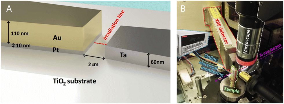 | ||
| Fig. 1 (A) Schematic layout of the metal contacts deposited on the TiO2 rutile single crystal to perform electrical characterizations. The dotted red line highlights the part of the sample that has been irradiated using the X-ray nanobeam. (B) Photograph of the experimental setup employed at the ESRF ID16B beamline showing the alignment optical microscope, the XRF detector and the sample mounted on the sample holder used for online electrical characterization. | ||
2.2. Electrical measurements
For online monitoring, the samples were mounted onto a sample holder compatible with the nanobeam experimental setup and connected with a two-terminal configuration to its contact pads by means of Ag wires 50 μm in diameter. The sample holder was interfaced through coaxial cables to a Keithley 6487 picoammeter/voltage source with high input impedance (1011 Ω) and good current resolution (10 fA) with high accuracy (0.3%). The acquisition was controlled by a computer via a GPIB employing a software program developed with LabVIEW. To acquire cyclic current–voltage characteristics, the sampling rate was set to 250 ms.2.3. X-ray nanobeam irradiation
X-ray irradiation was performed at the long-canted beamline ID16B-NA of the European Synchrotron Radiation Facility (ESRF) in Grenoble, France. The primary beamline optics are located next to the in-vacuum undulator source to preserve the coherence of the beam, while the Kirkpatrick–Baez mirrors, which act as focusing optics, are placed very close to the sample position (165 m far from the undulator source) to obtain a higher degree of demagnification. The experimental setup (Fig. 1B) includes an optical microscope to visualize the region of interest in the sample, a piezo positioning stage to raster-scan it under the X-ray nanoprobe and an energy dispersive Si drift detector to acquire the XRF signals.We operated in the pink beam mode without a double crystal monochromator (ΔE/E ≈ 10−2) to obtain a higher photon flux at the sample position. The X-ray nanopatterning procedure was performed at 17.5 keV with beam sizes at the focal plane of 65 × 58 nm2 (vertical × horizontal), as evaluated by the knife-edge scan method. The photon flux on the sample was 1.7 × 10¹¹ ph s−1. The XRF maps were collected with a counting time of 0.1 s per point using a 2 mm Si filter to avoid sample modifications.
2.4. Conductive atomic force microscopy
AFM and C-AFM maps were obtained using a Cypher S AFM from Asylum Research (Oxford Instruments Group) equipped with a dual gain ORCA cantilever holder. The two gains of the current amplifier of the cantilever holder were, respectively, 1 nA V−1 and 1 μA V−1. For conductive AFM measurements, an HQ:CSC17/AL-BS tip (n-type silicon) from μMasch was employed. During the acquisition of the C-AFM maps, the tip was grounded through the current amplifier and the sample was biased at 6 V through a 50 μm Ag wire connected to the Au electrode.2.5. Scanning electron microscopy
SEM images were acquired using an Inspect FTM electron microscope with a field emission gun (FEG) from FEI Company. Accelerating voltages from 5 to 30 kV were used.2.6. Transmission electron microscopy
TEM investigations were performed using a Tecnai F20 (Thermo Fisher Scientific Inc.), operated at 200 kV, with a TWIN objective lens (for the pristine sample) and a JEOL 2100 (JEOL, Ltd) instrument, operated at 200 kV, equipped with a high-resolution polepiece (for the irradiated sample). The TEM lamellas were extracted by the SEM-FIB technique using a TESCAN model LYRA 3 XMU instrument after coating the samples with a Pt conductive layer.3. Results and discussion
The devices under investigation were based on annealed TiO2 rutile single crystals with two series of electrical contacts (see Fig. 1A and the Experimental section): the first electrode, based on Ta, is expected to form an ohmic contact, while the second electrode, realized with Pt covered by Au, should give rise to a Schottky barrier. The gap between each couple of electrodes was 2 μm: this region was modified using the X-ray nanobeam to achieve the device resistive switching. The Ta/TiO2/Pt devices were mounted on a customized sample holder to perform in situ two-probe electrical measurement in the ESRF ID16B-NA nanobeam setup (Fig. 1B) to study the variations in the electrical conductivity of the sample after X-ray irradiation. After a preliminary alignment using an optical microscope (Fig. 1B), the region of interest in the sample was precisely located by X-ray fluorescence (XRF) maps.In the first step of our experiment, we “wrote” a single irradiation line connecting the Ta and Pt electrodes using the X-ray nanobeam with a step of 200 nm and an irradiation time of 25 s per point, resulting in a fluence of 9.9 × 10¹¹ J m−2. Then, we investigated the effect of the X-ray exposure by using atomic force microscopy (AFM) without performing any preliminary electrical characterization (i.e. no electrical bias has been applied to the device before the AFM measurements). The topographic map (Fig. 2A) shows a minimal local variation (<2 nm) in the height of the crystal induced by the exposure to the synchrotron nanobeam. On the other hand, the conductive atomic force microscopy (C-AFM) map (Fig. 2B) highlights the presence of a superficial conductive channel in the irradiated region. This behavior can be ascribed to the formation of oxygen vacancies in the TiO2 lattice, induced by the X-ray nanobeam. Indeed, the absorption of hard X-ray photons triggers the generation of photoelectrons, followed by de-excitation processes in the fs timescale which give rise to the production of fluorescence radiation and Auger electrons.22,23 The secondary and Auger electrons, while travelling in the oxide, produce electron–hole couples that can be responsible for knock-on and bond breaking processes.24–26 These phenomena have been previously studied by Monte Carlo simulations for superconducting oxides,26 showing that the secondary electrons can modify the sample properties for hundreds of nanometers around the X-ray nanobeam impact point, thus influencing the best spatial resolution that can be achieved in the X-ray nanopatterning process. Finally, at very high photon fluxes, as in our experiment, the scarcity of conduction electrons in insulating samples can slow down the restoration of the local electrical neutrality, inducing Coulomb repulsion between positive charges and subsequent ion ejection.24,27,28 All these phenomena can induce bond breaking, favouring the generation of point defects, essentially VO, which behave as n-dopants enhancing the local TiO2 conductivity.29,30 Conversely, local heating effects by the X-ray nanobeam, which were proven to be potentially relevant in modifying the oxygen content in superconducting oxides,8,31,32 are expected to be negligible for the TiO2 crystal.
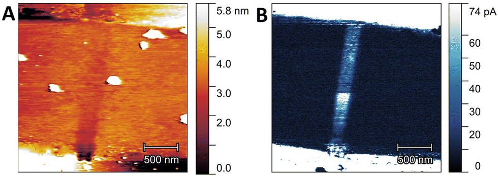 | ||
| Fig. 2 Topographic AFM (A) and current C-AFM (B) maps of the Ta/TiO2/Pt device after X-ray nanobeam irradiation without previously applying any bias. | ||
We moved then to investigate the effect of applying a voltage after realizing the irradiation line connecting the Ta and Pt metal contacts. Fig. 3A shows that, in a pristine sample, applying a voltage in the −30 V to 30 V range does not induce significant changes in the electrical properties (curve 1). Conversely, after X-ray nanobeam exposure, we observe a forming process (curve 2) which brings the sample to a LRS and then back to a HRS in the negative voltage range. Fig. 3B and C show the SET and RESET processes, typical of bipolar resistive switching.33 More I–V curves after multiple ON–OFF cycles, which show the reproducibility of the HRS and of LRS, are presented in Fig. S1 (ESI†). At a readout voltage of +1 V, the LRS resistance ranges between 6 and 7 kΩ, while the HRS varies between 14 and 17 kΩ. During the I–V measurements, the written states were stable over the observed time frame of a few minutes, demonstrating sufficient retention for this proof-of-principle experiment.
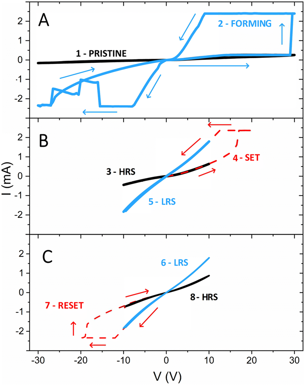 | ||
| Fig. 3 I–V curves of the Ta/TiO2/Pt device: (A) acquired before (curve 1) and after (curve 2) an X-ray irradiation line between two metal electrodes at maximum X-ray photon flux, inducing resistive switching; (B) readout of the high resistance state (HRS, curve 3), set process (curve 4) and readout of the low resistance state (LRS, curve 5); (C) readout of the LRS (curve 6), reset process (curve 7) and readout of the HRS (curve 8). | ||
The observed behaviour is significantly different with respect to previous experiments performed on Au/TiO2/Au samples where an increase of the material conductivity upon X-ray exposure was achieved, but no surface conductivity and reversible resistive switching were observed.9 This observation can be explained by the absence of ohmic contacts leading to lower initial VO concentration in the material and to lower currents flowing between the two Au electrodes with more limited migration of the VO created by the X-ray nanobeam and less intense Joule heating. It is also important to note that for photon fluxes <1010 ph s−1 (corresponding to an irradiance of ca. 8 × 10⁹ W m−2) we observe only a volatile resistance decrease due to the presence of photogenerated electrons, which is proportional to the photon flux and is completely reversible upon stopping the irradiation, as discussed in detail in our previous publication.9
Fig. 4 shows the SEM images of the Ta/TiO2/Pt device after the forming process. We can see an evident surface roughening in the tip of the Ta electrode, likely due to an oxidation process triggered by the high current flowing during the forming process. Moreover, we can note the presence of a bump between the electrodes in the region irradiated by the X-ray nanobeam.
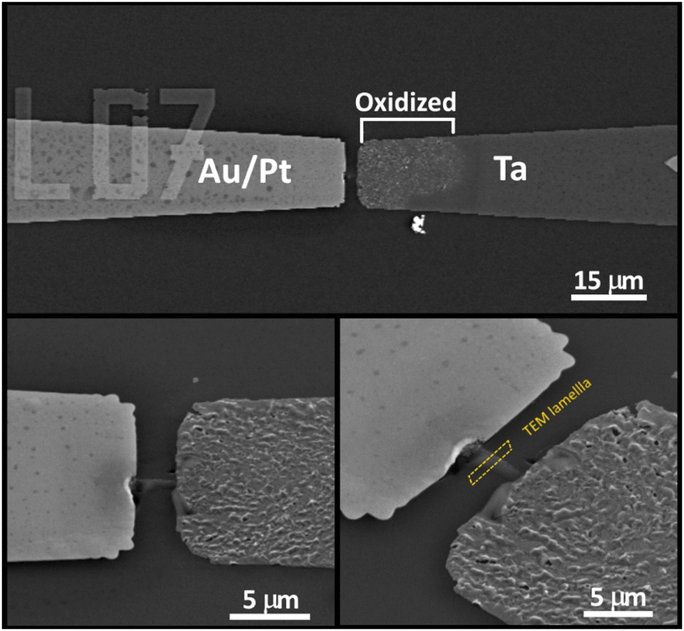 | ||
| Fig. 4 SEM images of the Ta/TiO2/Pt device after X-ray guided forming and electrical characterization (as shown in Fig. 3). The dotted yellow box highlights the part of the sample where the lamella for TEM analyses (see Fig. 6) has been cut. | ||
A more detailed investigation was then performed using atomic force microscopy (Fig. 5). Topographic maps (Fig. 5A) highlight a local increase in the height of the crystal of about 100 nm, centered on the irradiated line. The bump has a conical shape, already observed in previous TEM studies of conductive filaments generated by electroforming in Pt/TiO2/Pt stacks.34 Considering that the Ta contact was grounded, while the Pt one was positively biased during the forming process, we can infer that the voltage applied promoted a reorganization of the oxygen vacancies generated by the X-ray nanobeam with a significant local increase of the current density. The consequent temperature rise due to Joule heating favors the diffusion and generation of VO, which result in the growth of a conductive filament from the cathode toward the anode.35
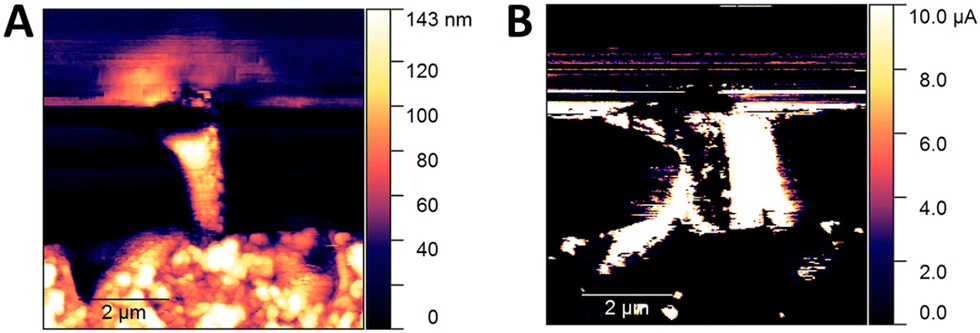 | ||
| Fig. 5 Topographic AFM (A) and current C-AFM (B) maps of the Ta/TiO2/Pt device after X-ray guided forming and electrical characterization (as shown in Fig. 3). | ||
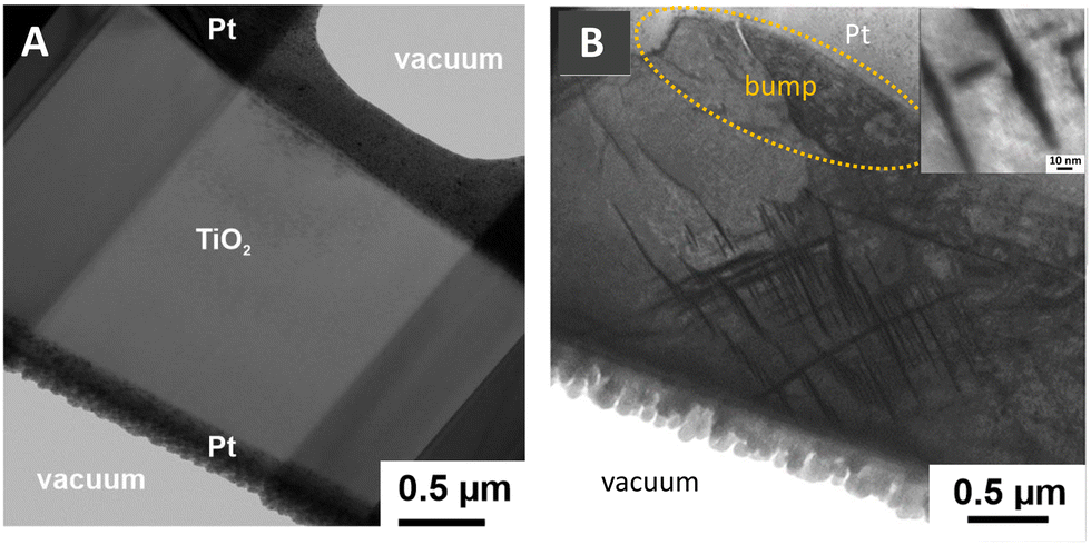 | ||
| Fig. 6 BF-TEM images of lamellas obtained by FIB milling from (A) a pristine TiO2 crystal and (B) the Ta/TiO2/Pt device after X-ray guided forming and electrical characterization (as shown in Fig. 3). The part of the sample where the lamella has been cut is shown in Fig. 4. In (B), the protective platinum layer deposited during the FIB milling process is brighter than the TiO2 crystal due to diffraction contrast. The bump region is highlighted by a dotted yellow ellipse. The inset shows a magnification of the dislocation region. | ||
Parallel C-AFM maps show (Fig. 5B) an increase in the surface conductivity of the TiO2 crystal, which is more evident in the borders of the bump. A previous study10 using space-resolved X-ray excited optical luminescence (XEOL) showed that these higher conductivity regions are associated with a lower intensity of a XEOL signal centered at 830 nm, which is attributed to the radiative recombination of electrons trapped in intra-band gap states with free holes in the valence band.36 These states have been ascribed to the presence of lattice defects like VO or Ti interstitials.37 Interestingly, it has been reported that an increasing concentration of VO is correlated to a decrease of this NIR photoluminescence emission36 since these defects provide a non-radiative recombination path to photoexcited electrons. Thus, we could infer that, following X-ray guided forming, a higher concentration of VO is induced in our device in the regions around the bump. This hypothesis would also explain the increase in the electrical conductivity observed in our samples, since a higher concentration of VO at the Pt/TiO2 interface lowers the Schottky barrier height, improving the injection of the charge carriers.38,39
Structural modifications occurring in the sample due to X-ray irradiation were investigated by BF-TEM analysis on a lamella cut by FIB milling (see the Experimental section) in the irradiated region, in the position shown in Fig. 4, to be compared with a similar lamella cut from a pristine TiO2 sample. From Fig. 6A, we can see that, as expected, the pristine crystal does not show any evidence of structural defects. Conversely, in the top part of Fig. 6B, the bump region can be identified (marked by a dotted white ellipse), as already highlighted by SEM and AFM. Moreover, in the subsurface region close to the bump, we can note the presence of a dislocation network, better visible in the inset of Fig. 6B. These structures can be compatible with the presence of Wadsley defects, which are shear faults induced by an increased concentration of VO, already observed in previous in situ TEM studies of rutile TiO2 resistive switching under electrical bias.40 This kind of defect has been reported to play an important role in the reduction process of TiO2, which can lead to the formation of a variety of Magneli phases with the general stoichiometry TinO2n−1.41,42 Indeed, according to the literature the process starts with the formation of some VO, which can be hosted in a limited amount into the rutile lattice, then the VO point defects start to aggregate along preferential crystallographic directions forming extended defects, which subsequently can possibly lead to a mixture of TinO2n−1 compounds with different n.43,44 Both experimental results and DFT calculations showed that ordered extended line defects, as the ones observed in Fig. 6B, allow electron conduction mediated by occupied defect states of Ti 3d character,45,46 in agreement with the results obtained by C-AFM.
4. Conclusions
By exploiting the ability of intense synchrotron radiation X-ray nanobeams to locally generate oxygen vacancies (VO) in oxides, we were able to realize conductive filaments in desired positions of our TiO2 crystals between the Pt and Ta metal contacts. The successive application of suitable voltage pulses allowed us to order the X-ray induced VO, achieving a significant local increase of the current density with associated Joule heating. This process favors the diffusion and generation of VO, which leads to the growth of a conductive filament from the cathode toward the anode suitable for the device fabrication (for a complete scheme of the different steps of the X-ray nanopatterning process, see Fig. S2 in the ESI†). The I–V curves recorded after this electroforming procedure showed bipolar resistive switching. Moreover, (C-)AFM maps acquired on the final Ta/TiO2/Pt device highlighted a local increase in the height of the crystal in the irradiated region, associated with a decrease of the surface electrical resistivity. BF-TEM analysis in the filament region confirms the formation of a dislocation network, ascribed to the aggregation of VO point defects along preferential crystallographic directions to form extended line defects, which are involved in the increased electrical conduction. These structures are compatible with the presence of Wadsley defects, which can possibly lead to the formation of Magneli phases.The X-ray guided forming protocol discussed in this paper, although it was limited to a proof of concept and was not employed for the fabrication of a specific electronic device, can create new opportunities for fabricating oxide-based memristive devices. Specifically, this method could be utilized in future systematic studies to enhance process control and reduce the device-to-device variability possibly arising from conventional electroforming. Moreover, this study further confirms that the X-ray nanopatterning technique can be an effective tool for the nanofabrication of oxides, able to locally increase or decrease the material conductivity.
Author contributions
Lorenzo Mino: conceptualization, investigation, visualization, writing – original draft; Valentina Bonino: investigation, writing – review & editing, visualization; Andrea Alessio: investigation; Federico Picollo: investigation, visualization; Andrei Kuncser: investigation; Ionel Mercioniu: investigation; Aurel-Mihai Vlaicu: investigation; Petre Badica: investigation, writing – review & editing; Rosaria Brescia: investigation, visualization; Matteo Fretto: investigation; Kalle Goss: investigation; Regina Dittmann: conceptualization, supervision; Marco Truccato: investigation, conceptualization, supervision.Data availability
The data are available from the corresponding author upon reasonable request.Conflicts of interest
There are no conflicts to declare.Acknowledgements
The authors thank the European Synchrotron Radiation Facility (ESRF) for allocation of beamtime at the beamline ID16B, for AFM support at the Partnership for Soft Condensed Matter (PSCM), and for the kind availability of all its staff. L. M. acknowledges the support from the Project CH4.0 under the MUR program “Dipartimenti di Eccellenza 2023-2027” (CUP: D13C22003520001). P. B., I. M., and A. K. acknowledge the support from the Ministry of Research, Innovation and Digitalization through Core Program PC1-PN23080101 and PC2-PN23080101. R. D. and K. G. acknowledge the grant SFB 917 “Nanoswitches” of the German Science Foundation (DFG) for funding.References
- S. Okazaki, Microelectron. Eng., 2015, 133, 23–35 CrossRef CAS.
- E. Sharma, R. Rathi, J. Misharwal, B. Sinhmar, S. Kumari, J. Dalal and A. Kumar, Nanomaterials, 2022, 12, 2754 CrossRef CAS PubMed.
- J. R. Maldonado and M. Peckerar, Microelectron. Eng., 2016, 161, 87–93 CrossRef CAS.
- F. Romanato, L. Businaro, L. Vaccari, S. Cabrini, P. Candeloro, M. De Vittorio, A. Passaseo, M. T. Todaro, R. Cingolani, E. Cattaruzza, M. Galli, C. Andreani and E. Di Fabrizio, Microelectron. Eng., 2003, 67–8, 479–486 CrossRef.
- F. Cerrina, J. Phys. D: Appl. Phys., 2000, 33, R103–R116 CrossRef CAS.
- M. Truccato, A. Agostino, E. Borfecchia, L. Mino, E. Carat, A. Pagliero, N. Adhlakha, L. Pascale, L. Operti, E. Enrico, N. De Leo, M. Fretto, G. Martinez-Criado and C. Lamberti, Nano Lett., 2016, 16, 1669–1674 CrossRef CAS PubMed.
- A. Pagliero, L. Mino, E. Borfecchia, M. Truccato, A. Agostino, L. Pascale, E. Enrico, N. De Leo, C. Lamberti and G. Martinez-Criado, Nano Lett., 2014, 14, 1583–1589 CrossRef CAS PubMed.
- L. Mino, V. Bonino, A. Agostino, C. Prestipino, E. Borfecchia, C. Lamberti, L. Operti, M. Fretto, N. De Leo and M. Truccato, Sci. Rep., 2017, 7, 9066 CrossRef PubMed.
- L. Mino, V. Bonino, F. Picollo, M. Fretto, A. Agostino and M. Truccato, Adv. Electron. Mater., 2019, 5, 1900129 CrossRef.
- A. Alessio, V. Bonino, T. Heisig, F. Picollo, D. Torsello, L. Mino, G. Martinez-Criado, R. Dittmann and M. Truccato, Phys. Status Solidi RRL, 2021, 15, 2100409 CrossRef CAS.
- J. J. S. Yang, D. B. Strukov and D. R. Stewart, Nat. Nanotechnol., 2013, 8, 13–24 CrossRef CAS PubMed.
- M. A. Zidan, J. P. Strachan and W. D. Lu, Nat. Electron., 2018, 1, 22–29 CrossRef.
- R. Dittmann and J. P. Strachan, APL Mater., 2019, 7, 110903 CrossRef.
- X. Duan, Z. Cao, K. Gao, W. Yan, S. Sun, G. Zhou, Z. Wu, F. Ren and B. Sun, Adv. Mater., 2024, 36, 2310704 CrossRef CAS PubMed.
- B. Sun, Y. Chen, G. Zhou, Z. Cao, C. Yang, J. Du, X. Chen and J. Shao, ACS Nano, 2024, 18, 14–27 CrossRef CAS PubMed.
- K. X. Sun, J. S. Chen and X. B. Yan, Adv. Funct. Mater., 2021, 31, 2006773 CrossRef CAS.
- S. Kim, S. Choi and W. Lu, ACS Nano, 2014, 8, 2369–2376 CrossRef CAS PubMed.
- S. Menzel, U. Bottger, M. Wimmer and M. Salinga, Adv. Funct. Mater., 2015, 25, 6306–6325 CrossRef CAS.
- J. H. Yoon, J. M. Zhang, X. C. Ren, Z. R. Wang, H. Q. Wu, Z. Y. Li, M. Barnell, Q. Wu, L. J. Lauhon, Q. F. Xia and J. J. Yang, Adv. Funct. Mater., 2017, 27, 9 Search PubMed.
- C. Baeumer, R. Valenta, C. Schmitz, A. Locatelli, T. O. Mentes, S. P. Rogers, A. Sala, N. Raab, S. Nemsak, M. Shim, C. M. Schneider, S. Menzel, R. Waser and R. Dittmann, ACS Nano, 2017, 11, 6921–6929 CrossRef CAS PubMed.
- M. Rao, H. Tang, J. Wu, W. Song, M. Zhang, W. Yin, Y. Zhuo, F. Kiani, B. Chen, X. Jiang, H. Liu, H. Y. Chen, R. Midya, F. Ye, H. Jiang, Z. Wang, M. Wu, M. Hu, H. Wang, Q. Xia, N. Ge, J. Li and J. J. Yang, Nature, 2023, 615, 823–829 CrossRef CAS PubMed.
- L. Mino, G. Agostini, E. Borfecchia, D. Gianolio, A. Piovano, E. Gallo and C. Lamberti, J. Phys. D: Appl. Phys., 2013, 46, 423001 CrossRef.
- L. Mino, E. Borfecchia, J. Segura-Ruiz, C. Giannini, G. Martinez-Criado and C. Lamberti, Rev. Mod. Phys., 2018, 90, 025007 CrossRef CAS.
- J. Cazaux, J. Microsc., 1997, 188, 106–124 CrossRef CAS.
- S. P. Hau-Riege, High-Intensity X-Rays Interaction with Matter, Wiley-VCH, Weinheim, 2011 Search PubMed.
- D. Torsello, L. Mino, V. Bonino, A. Agostino, L. Operti, E. Borfecchia, E. Vittone, C. Lamberti and M. Truccato, Phys. Rev. Mater., 2018, 2, 014801 CrossRef CAS.
- M. L. Knotek and P. J. Feibelman, Surf. Sci., 1979, 90, 78–90 CrossRef CAS.
- S. Tanaka, K. Mase and S. Nagaoka, Surf. Sci., 2004, 572, 43–58 CrossRef CAS.
- P. Knauth and H. L. Tuller, J. Appl. Phys., 1999, 85, 897–902 CrossRef CAS.
- M. K. Nowotny, T. Bak and J. Nowotny, J. Phys. Chem. B, 2006, 110, 16270–16282 CrossRef CAS PubMed.
- L. Mino, E. Borfecchia, A. Agostino, C. Lamberti and M. Truccato, J. Electron Spectrosc. Relat. Phenom., 2017, 220, 69–75 CrossRef CAS.
- V. Bonino, D. Torsello, C. Prestipino, L. Mino and M. Truccato, J. Synchrot. Radiat., 2020, 27, 1662–1673 CrossRef PubMed.
- D. S. Jeong, H. Schroeder and R. Waser, Electrochem. Solid-State Lett., 2007, 10, G51–G53 CrossRef CAS.
- D. H. Kwon, K. M. Kim, J. H. Jang, J. M. Jeon, M. H. Lee, G. H. Kim, X. S. Li, G. S. Park, B. Lee, S. Han, M. Kim and C. S. Hwang, Nat. Nanotechnol., 2010, 5, 148–153 CrossRef CAS PubMed.
- K. C. Tang, A. C. Meng, F. Hui, Y. Shi, T. Petach, C. Hitzman, A. L. Koh, D. Goldhaber-Gordon, M. Lanza and P. C. McIntyre, Nano Lett., 2017, 17, 4390–4399 CrossRef CAS PubMed.
- D. K. Pallotti, L. Passoni, P. Maddalena, F. Di Fonzo and S. Lettieri, J. Phys. Chem. C, 2017, 121, 9011–9021 CrossRef CAS.
- S. Wendt, P. T. Sprunger, E. Lira, G. K. H. Madsen, Z. S. Li, J. O. Hansen, J. Matthiesen, A. Blekinge-Rasmussen, E. Laegsgaard, B. Hammer and F. Besenbacher, Science, 2008, 320, 1755–1759 CrossRef CAS PubMed.
- Y. G. Zhou, Z. Z. Zhang, Z. W. Fang, M. Qiu, L. Ling, J. L. Long, L. Chen, Y. C. Tong, W. Y. Su, Y. F. Zhang, J. C. S. Wu, J. M. Basset, X. X. Wang and G. H. Yu, Proc. Natl. Acad. Sci. U. S. A., 2019, 116, 10232–10237 CrossRef CAS PubMed.
- T. Tamura, S. Ishibashi, K. Terakura and H. M. Weng, Phys. Rev. B: Condens. Matter Mater. Phys., 2009, 80, 195302 CrossRef.
- R. J. Kamaladasa, A. A. Sharma, Y. T. Lai, W. Chen, P. A. Salvador, J. A. Bain, M. Skowronski and Y. N. Picard, Microsc. Microanal., 2015, 21, 140–153 CrossRef CAS PubMed.
- K. Szot, C. Rodenbücher, G. Bihlmayer, W. Speier, R. Ishikawa, N. Shibata and Y. Ikuhara, Crystals, 2018, 8, 241 CrossRef.
- Y. Liu, J. Yang, Y. Liu, J. Zheng, W. Lee, J. Shi, J. Horlyck, J. Xie, Y. Y. Tay, T. T. Tan, D. Yu, R. Mole, G. McIntyre, C. Zhang, C. Y. Toe, T. D. Waite, J. Scott, Y. Wang, T. Wu, S. Han and S. Li, Energy Environ. Sci., 2020, 13, 5080–5096 RSC.
- K. Szot, M. Rogala, W. Speier, Z. Klusek, A. Besmehn and R. Waser, Nanotechnology, 2011, 22, 254001 CrossRef CAS PubMed.
- X. Wu, N. Yang, Y. Ji, X. He, Q. Li, R. Jiang, Z. Lei, Z. Liu and J. Sun, CrystEngComm, 2023, 25, 1146–1158 RSC.
- S. G. Park, B. Magyari-Kope and Y. Nishi, IEEE Electron Device Lett., 2011, 32, 197–199 CAS.
- M. Rogala, G. Bihlmayer, W. Speier, Z. Klusek, C. Rodenbücher and K. Szot, Adv. Funct. Mater., 2015, 25, 6382–6389 CrossRef CAS.
Footnote |
| † Electronic supplementary information (ESI) available. See DOI: https://doi.org/10.1039/d4tc01815j |
| This journal is © The Royal Society of Chemistry 2024 |