
Contactless pressure detection enabled by a hybrid 3D laser-printed nanophotonic sensor†
Francesca Romana
Calabrò
ab,
Krzysztof
Mackosz
a,
Anna
Theodosi
cd,
Ioannis
Katsantonis
cd,
Ivo
Utke
a,
Maria
Kafesaki
cd,
Maria Gabriella
Santonicola
 b,
Johann
Michler
a,
Angelos
Xomalis‡
*ae and
Jakob
Schwiedrzik‡
*a
b,
Johann
Michler
a,
Angelos
Xomalis‡
*ae and
Jakob
Schwiedrzik‡
*a
aLaboratory for Mechanics of Materials and Nanostructures, Empa, Swiss Federal Laboratories for Materials Science and Technology, Thun 3602, Switzerland. E-mail: jakob.schwiedrzik@empa.ch
bDepartment of Chemical Engineering Materials Environment, Sapienza University of Rome, Via del Castro Laurenziano 7, Rome 00161, Italy
cInstitute of Electronic Structure and Laser (IESL), Foundation for Research and Technology-Hellas (FORTH), Heraklion 70013, Greece
dDepartment of Materials Science and Technology, University of Crete, Heraklion 70013, Greece
eNanoelectronics and Photonics Group, Department of Electronic Systems, Norwegian University of Science and Technology, Trondheim 7034, Norway. E-mail: angelos.xomalis@ntnu.no
First published on 4th September 2024
Abstract
Modern wearable pressure sensors rely on converting external stimuli to electrical signals. Despite being widely developed, they still present significant disadvantages such as intrinsic heat generation due to electrical losses, which can interfere with data acquisition, limited speed of electronics, and user discomfort. Here, we propose a nanophotonic approach in which mechanical loading alters the optical behavior of photonic nanostructures. Using direct laser writing, we fabricate three-dimensional photonic structures on flexible substrates. These are coated with ZnO using atomic layer deposition enhancing their optical properties and biocompatibility. Exploiting full-wave photothermal and electromagnetic simulations, we induce a thermal conductance mismatch via a layered substrate to avoid photo-induced thermal damage of the substrate during writing and engineer the optical resonances of the sensor in the telecommunication C-band. Imitating pressure variations in the human body, we integrate our photonic device into a bulge setup to apply biaxial loading and monitor the changes of optical properties in situ. We show the potential of the technology for strain sensing applications with a sensitivity of 0.016% under cyclic loading. This study thus aims to support future investigations combining nanofabrication and coating techniques with the aim of developing biocompatible all-optical sensors for low-loss and ultrafast wearable diagnostics.
 Angelos Xomalis | Angelos joined Norwegian University of Science and Technology as an Associate Professor of Optical Engineering and Nanophotonics in 2023. Angelos pursues interdisciplinary research where fundamental science meets hybrid nanomaterials for developing a new class of classical and quantum meta-devices for novel sensing methodologies. He obtained his BA and MSc degrees from the Department of Materials Science and Technology, University of Crete and his PhD from the Optoelectronics Research Centre, University of Southampton. Then he was a Research Fellow at the Cavendish Laboratory, University of Cambridge and a Researcher at the Swiss Federal Laboratories for Materials Science and Technology. |
Introduction
Real-time diagnostics of the human body processes has become extremely important as it promises a constant data stream for early diagnosis and treatment of diseases.1,2 Flexible sensors emerge as a powerful technology to carry out this task. Their wide implementation in modern detection architectures allows for more effective and patient-friendly diagnostics. There are key factors that a wearable sensor should fulfil. It should be biocompatible, thin, lightweight, and provide an appropriate sensing range and sensitivity.3 The vast majority of the current wearable sensors are based on the detection of electrical signals upon an external stimulus such as the heart rate, wrist pulse, or blood/intraocular pressure variation,4i.e. they involve pressure detectors. To fulfil the necessity of requiring maximum efficiency, sensitivity, and precision, the advent of nanophotonics has attracted considerable attention. Studying the fundamental light–matter interaction, nanophononics provides a new pathway in wearable sensor development for real-time non-invasive diagnostics.Over the last two decades, pressure and strain detection devices have attracted considerable attention due to their wearability and mechanical stability, providing cost-effectiveness and long device life span.5 To date, pressure sensors are typically based on force-induced changes in piezo-resistivity, capacitance, and piezo- and tribo-electricity.6 Such sensors transduce an external pressure stimulus into electrical signals.7 Despite having demonstrated high sensitivity and capability for human health monitoring, many challenges remain to be addressed. Briefly, for a piezoresistive sensor, in vivo measures require enhanced adhesion and a relatively large contact area. A capacitive sensor does not exhibit high sensitivity for the entire range of pressure measurements.8 Moreover, the abovementioned sensors are not self-powered. Piezoelectric and triboelectric devices deliver good response time and sensitivity; however, when converting mechanical energy into electricity they are limiting the potential of wearable sensors due to their low mechanical toughness.9–11 Furthermore, a significant aspect to take into account is electrical losses that can interfere with data collection, limited acquisition and speed (due to electronics) and generation of thermal gradients, thus resulting in localized temperature rise, which is potentially harmful for patients.
In the broad range of commercialized sensor devices, only a small portion is optical-based. One measurement principle used today is based on the detection of a spectrum shift induced by mechanical deformation with the use of a photonic sensor such as a ring resonator or a 2D photonic crystal.12 Other approaches include photonic crystal waveguides13 enabling the detection of mechanical load by measuring the shifted resonance wavelength. Since shifting the wavelength resulted in leaving the telecommunication band, the idea behind these devices has certain limitations. Furthermore, optical devices based on fibre Bragg gratings (FBGs)5 use the concept of creating a grating area in an optical fibre at a specific position with a periodic distribution of the refractive index. To overcome the challenges of the state-of-the-art pressure sensors and explore the potential of optical-based sensors, the integration of nanophotonic principles into flexible pressure sensors stands as a novel approach that offers several advantages including improved sensitivity, miniaturization, and contactless operation.
Here, we propose a three-dimensional (3D) direct-laser-writing (DLW) photonic crystal (woodpile, WD) structure, printed directly onto a thin and flexible polyimide (PI) substrate (Fig. 1a) for pressure detection. DLW is an emerging method for laser 3D printing, which combines the advantages of a maskless technique with the capability of creating structures below the diffraction limit of light. Photonic crystals (PCs), i.e. photonic structures, consisting of periodically arranged materials, establish strong interactions with the incident light, thus leading to sensing functions with high efficiency.14 Specifically, the optical response of PCs is associated with resonances which can be extremely sensitive, among others, to small variations of the structure geometry, such as pressure-induced variations/deformations. This makes properly designed and engineered PCs excellent candidates for pressure/strain sensing, as is demonstrated in the present work. To date, there is no report on a similar device in the literature that brings together innovative 3D laser printer nanofabrication, a flexible substrate and pressure detection based on reflection intensity changes within the telecommunication band.
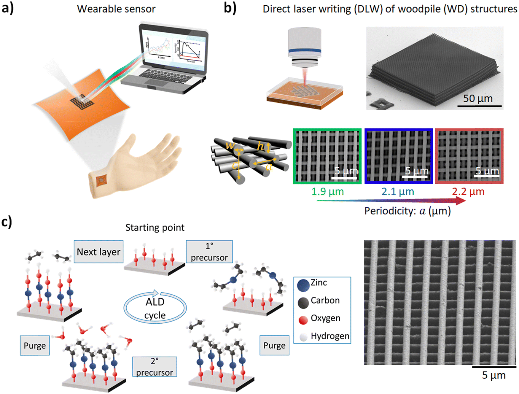 | ||
| Fig. 1 Pressure detection enabled by laser-printed 3D biocompatible nanophotonic structures coated by atomic layer deposition (ALD). (a) Example of pressure detection by monitoring changes in the optical properties of a laser-printed nanophotonic structure on a flexible polyimide substrate. (b) Direct laser writing (DLW) of woodpile (WD) structures (116 × 116 μm2) through a photosensitive material on flexible substrates (∼20 μm, top left), SEM images of the resulting structure (top right), and structures of three periodicities (a = 1.9, 2.1, and 2.2 μm, bottom). The inset shows the structural parameters w = h = 0.46 μm, c = 1.84 μm and a of the WD unit cell. (c) ALD process of ZnO (left) and SEM image of the resulting coated structure (right). | ||
The photonic crystals designed and investigated here are WD structures with resonant response in the telecommunication C-band (∼1.5 μm; Fig. 1b) essential for compatibility with standard optical communication platforms. The design of the structures is performed using full-wave electromagnetic simulations, where different periodicities are considered to achieve fine tuning of optical resonances within the desired C-band. To be able to fabricate the structures on a flexible substrate, essential for their implementation in a wearable pressure sensor scheme, we perform investigations employing full-wave photothermal simulations and derive an approach and conditions to realize fabrication avoiding the associated laser-induced photothermal damage. After structure fabrication via DLW, exploiting atomic layer deposition (ALD), we conformally coat the WDs with an 80 nm layer of zinc oxide (ZnO) to alter their apparent optical properties and enable sensor biocompatibility (Fig. 1c). Furthermore, we perform in situ monitoring of optical properties upon mechanical loading; mimicking the pressure variation in the human body, we integrate our photonic structure (strain sensor) into a custom-built bulge setup and evaluate the pressure detection performance. We repeat the evaluation over 1000 loading cycles, demonstrating the structure-response robustness, essential for real-life applications.
Results and discussion
DLW is a large-scale and cost-effective method of printing nanoscale structures, with feature sizes below 100 nm. For those structures working as wearable pressure sensors, it is essential for them to be placed on top of flexible substrates. While DLW delivers high-resolution sensors, performing laser fabrication directly on PI induces photothermal damage due to high absorption in the UV range (2-photon absorption wavelength; Fig. 2a). To evaluate this behavior, we perform full-wave photothermal simulations. First, we exploit a thin film (40 nm) of Au on top of PI to increase the reflectivity of the surface (essential for finding the interface during DLW; see Fig. 2b). However, Au has high optical absorption combined with good heat conductance (397 W mK−1), leading to elevated photothermal heating and resulting in thermal gradients as high as 350 K (top right, Fig. 2c). To avoid this, we add an intermediate thin layer of carbon (C, 30 nm; between Au and PI) with the aim to induce a heat conductance mismatch. This indeed leads to lower optical absorption (Pabs) and a drastic reduction of the resulting thermal gradient (∼ΔT = 5 K, bottom right of Fig. 2c). Consequently, based on our simulation study, we deposit the Au/C layered substrate via sputtering. This allows the fabrication of WDs via DLW without unwanted thermal damage of the polymeric flexible substrate.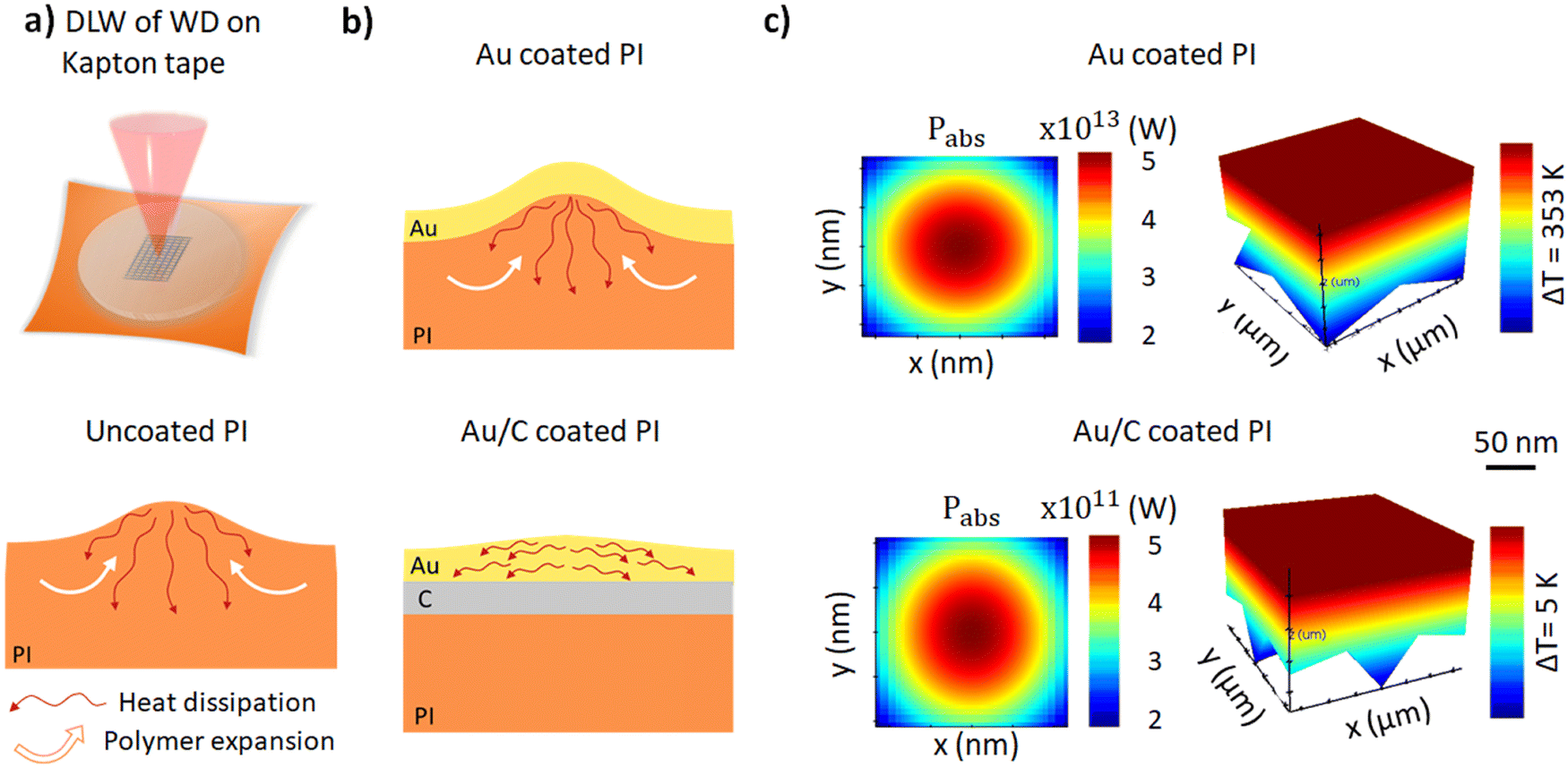 | ||
| Fig. 2 Photothermal study for direct laser printing on flexible substrates. (a) (Top) DLW for the fabrication of WDs on Kapton tape (polyimide, PI). (Bottom) PI absorbs strongly in the UV range (two-photon absorption wavelength) leading to material expansion due to thermal damage. (b) (Top) First approach using an Au thin layer (40 nm) to increase the reflectivity (essential for finding the interface). (Bottom) Second approach using a C interlayer (30 nm) as a heat-insulating layer between Au and PI. (c) Photothermal simulations for (top) Au–PI and (bottom) Au–C–PI layered structures. (Left) Power absorbed maps in the PI cross-section as a result of the optical absorption which is converted (right) to a thermal gradient. | ||
The photonic structure response of WDs depends strongly on their structural parameters. One such critical parameter is structure periodicity. Here we investigate (design, fabricate, and characterize) three different periodicities (structures are shown in Fig. 1b) to fully cover the desired telecommunication range: 1.9, 2.1 and 2.2 μm. The DLW-obtained polymeric structures are subsequently coated with ZnO (thickness of 80 ± 5 nm) via ALD (Fig. 1c). The reflection spectra of the fabricated structures (coated and uncoated) are shown in Fig. 3. As can be seen from Fig. 3a, the uncoated structures show flat reflection spectra throughout the NIR detection range, as expected due to the low refractive index of the resist (IP-dip, Nanoscribe). In contrast, as the refractive contrast (with air) increases, the ZnO-coated (80 nm) structures show clear periodicity-dependent resonances in reflection, where the resonance is shifted for about 200 nm (from 1450 to 1650 nm) with the abovementioned periodicity change (Fig. 3b).
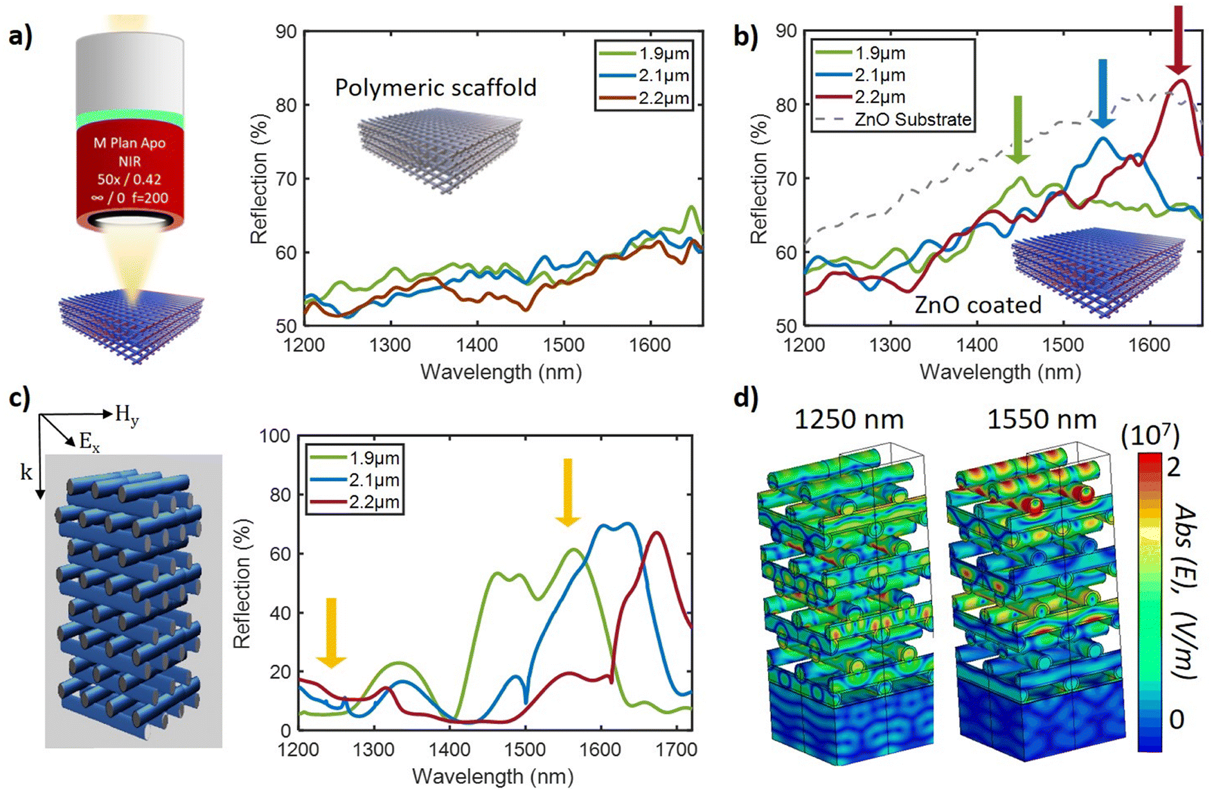 | ||
| Fig. 3 Engineering the optical properties of laser-printed ZnO-coated 3D photonic structures on flexible substrates. Optical properties measured with a reconfigurable optical microscope including a near-infrared (NIR) spectrometer. Experimental measurements of 1.9 (green), 2.1 (blue), and 2.2 μm (red) periodicities of (a) polymeric (uncoated) and (b) ZnO-coated woodpiles (WDs). (c) Simulated reflection spectra considering finite layers in the z-axis and periodic boundary conditions in the x- and y-axis. (d) Electric-field 3D maps of the 1.9 μm periodicity WD at a wavelength of (left) 1250 and (right) 1550 nm. | ||
To better understand the nature of the resonances and their periodicity dependent shifts, we perform full-wave simulations (CST Studio Suite; Fig. 3c and d). Here, we consider four unit cells along the propagation direction (z-direction; see Fig. 3d) and ‘unit cell’ periodic boundary conditions in the lateral directions (x and y). We plot in Fig. 3c the simulated normalized reflection of 1.9 (green line), 2.1 (blue), and 2.2 μm (red) periodicities, with impinging light at normal incidence, as shown in Fig. 3a. Similarly to the experiment, the reflection resonance is shifted from a wavelength of about 1500 to 1700 nm. To understand the origin of the observed reflection resonances/peaks, we plot the electric-field distribution in 3D maps showing the mode profile and light localisation for the 1.9 μm periodicity WD. At a 1250 nm wavelength (off-resonance), the incident wave penetrates the structure of the WDs, and the electric-field is distributed throughout the structure almost uniformly. On resonance (1550 nm), the electric field shows distinct nodes along the propagation direction, resembling the field profile at the Bragg-gaps of the photonic crystal, associated with the reflection peak, in good agreement with the experiment.
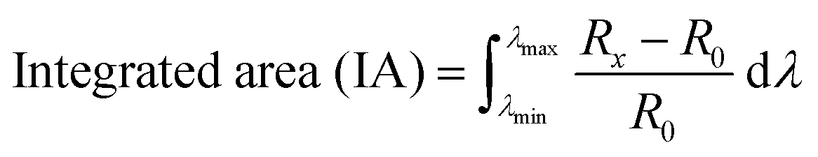
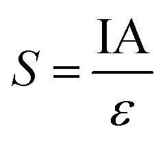
After achieving enhanced optical properties, the next task is to test the meta-device sensitivity upon mechanical loading. Imitating human body pressure variations, we load the photonic meta-device into a bulge setup to perform in situ optical measurements while varying the pressure. For each pressure step, we record the reflection spectra with a custom-built optical microscope comprising a NIR spectrometer (Fig. 4a). To test the pressure sensitivity, we measure the reflection spectra of the three WD periodicities (1.9, 2.1 and 2.2 μm) during inflation and deflation (left and middle, Fig. 4b). Different shades of colours in the spectra stand for measurements under different pressure values (see colour bars in Fig. 4). Next, we calculate the integrated area (IA) by integrating the reflection spectra between two pressure values: initially at 0 pressure (ΔP = 0 bar) and x pressure (ΔP = x bar) steps for a range of wavelengths between λmin = 1400 nm and λmax = 1600 nm (right, Fig. 4b). In the formula shown below, R0 represents the reflection at pressure ΔP = 0 bar and Rx represents the reflection at pressure ΔP = x bar:
 | (1) |
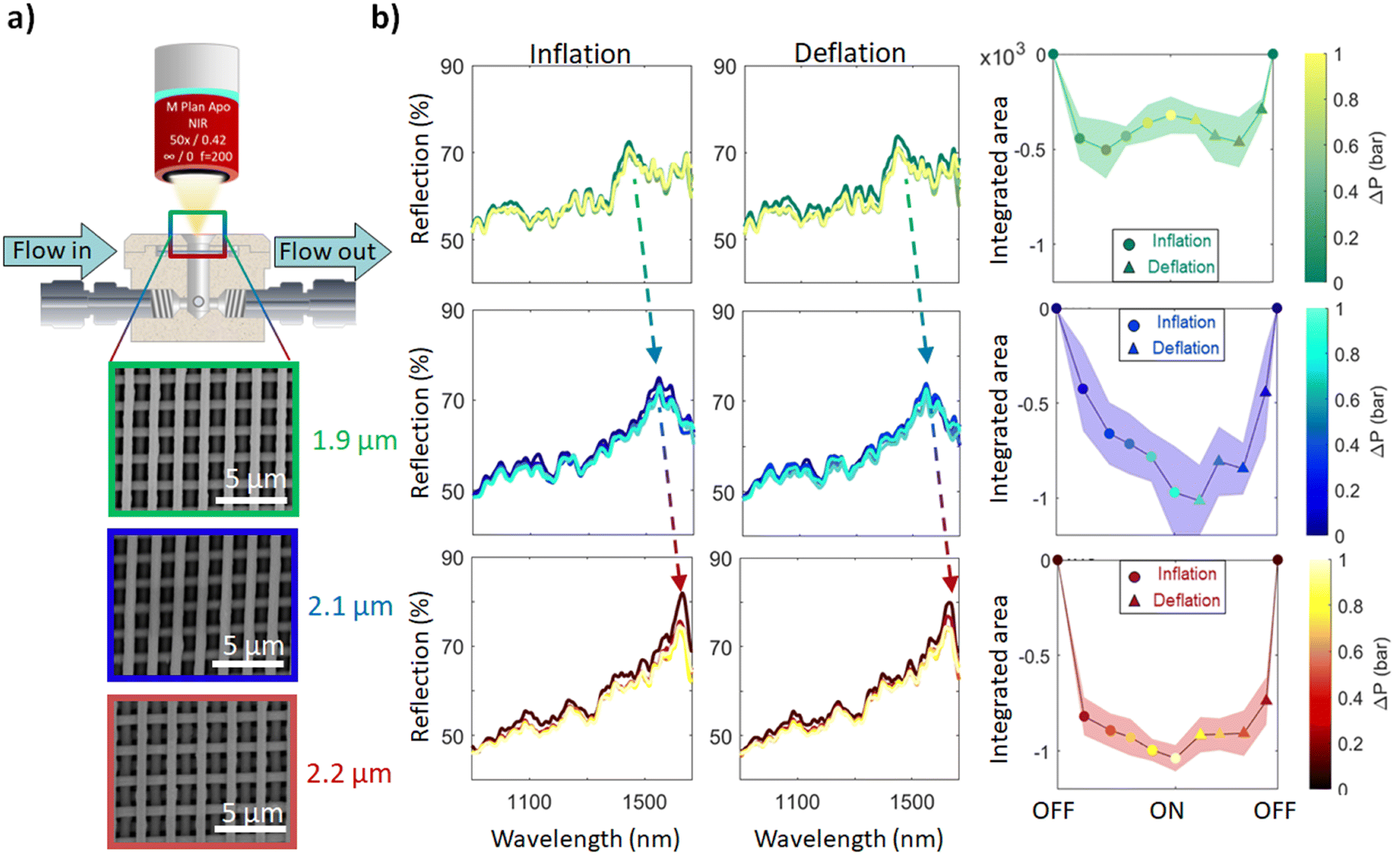 | ||
| Fig. 4 Analysis of pressure variation detection by monitoring changes in optical properties for WD periodicities. (a) In situ pressure bulge setup for measuring the optical properties of WDs with 1.9 (green), 2.1 (blue), and 2.2 μm (red) periodicities. (b) Reflection spectra of three periodicities recorded during inflation (left) and deflation (middle) and the resulting pressure sensitivity performance (right). Faded colours stand for measurement errors. Arrows indicate the resonance position. | ||
Every point (see the third column in Fig. 4b) corresponds to differential reflection for each pressure step under inflation (circular markers) and deflation (triangular markers). Shade colours stand for the measurement error. A similar behavior is observed for continuous loading/pressure cycling, demonstrating that the 2.2 WD structure shows the best pressure sensitivity performance (Fig. S1, ESI†).
As shown in Fig. 4b, our structures demonstrate variable pressure detection sensitivity with rising periodicity, in particular an increase in pressure sensitivity performance as the periodicity increases (from top to bottom), quantified by the integrated area value. Especially, the small peak of the differential integrated area at the minimum point (at the highest-pressure value of ΔP = 1 bar) in 1.9 μm (green, Fig. 4b left) is absent in 2.1 (blue) and 2.2 μm (red) periodicities. The integrated area values are −320 ± 98 for 1.9 μm periodicity, −970 ± 244 for 2.1 μm and −1038 ± 69 for 2.2 μm periodicity (see the right panel of Fig. 4b). Furthermore, the most symmetrical trends for both inflation and deflation and the largest reduction of the integrated area of differential reflection and the smallest errors are observed for 2.2 μm periodicity. For the latter periodicity, our measurements show that the best performance is observed when the resonance of the structure is slightly red-shifted with respect to the integration window. Further studies might concern the fine tuning of resonances across the targeted wavelengths for the evaluation of the detection sensitivity; this might be more pronounced considering higher refractive index dielectrics (n > 3) where the resonance should be appearing more narrowband (higher Q-factors). Importantly, the biocompatibility of the material should be preserved.
To evaluate the potential of our laser-printed photonic pressure sensor for real-life diagnostics and assess the repeatability of pressure sensitivity, we investigate the changes of optical properties by a fatigue test. Particularly, we perform 1000 cycles of mechanical loading (consecutive inflation/deflation) and measure the integrated area at 100, 500, and 1000 cycles (Fig. 5a and b). We note that the time of measurement is increased for having enough time for data acquisition and every measurement comprises four repeats for clarity (left, Fig. 5a). Furthermore, we plot the reduction of the integrated area for 0, 100, 500 and 1000 cycles for an applied pressure of 1 bar (Fig. 5c). After 1000 cycles, the integrated area is reduced by 34% (Fig. 5c). This reduction in signal is likely caused by inelastic deformation of the flexible substrate and may be minimized in future studies by reducing the applied strain on the membrane.
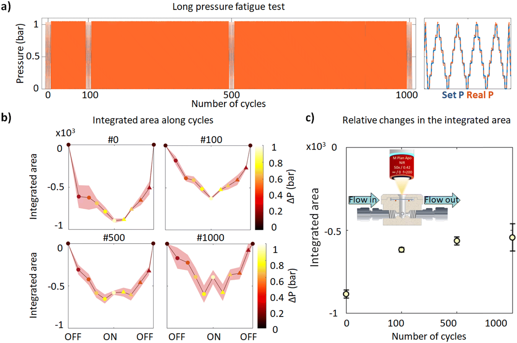 | ||
| Fig. 5 Fatigue pressure detection measurement. (a) Fatigue test with four measured spots at 0, 100, 500, and 1000 cycles (left) and an example of the four measurement repeats around each spot (right). (b) Differential integrated area of the reflection spectra for a wavelength between 1400 and 1600 nm. (c) Relative changes in the integrated area over a different number of cycles (measured at 0, 100, 500, and 1000 cycles). | ||
The aim here is to design an all-optical wearable sensor for detection of pressure in the human body. Ideally for such diagnostics the sensor needs to detect small pressure variations. To evaluate the maximum sensitivity of our setup, we calculate the strain developed at the structure point as we inflate the membrane. Here, we consider the approximation for a circular membrane for calculating strain and stress.15–17 Briefly, for a membrane with a radius of a = 0.5 cm and an applied pressure of p = 0.2 bar, displacement in the z-axis of h ≅ 77 μm and t = 25 μm membrane (Kapton tape) thickness, we calculate a stress 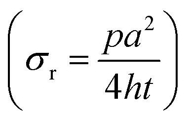 of 65 MPa and a strain
 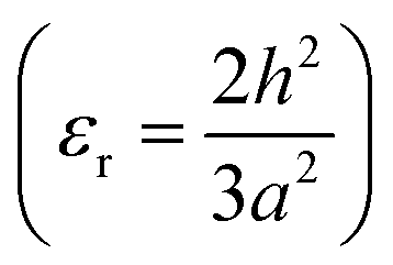 of 0.016% for circular geometry according to the analytical model of Vlassak et al.18 When we perform the same calculations at p = 1 bar, taking into account a displacement of h = 183 μm, we find that the stress would rise up to 136.5 MPa, which corresponds to a strain of 0.089% under the assumption of linear elastic behaviour. As this stress surpasses the yield stress of polyimide (73 MPa), the loading of the membrane likely resulted in plastic deformation of the substrate. It is therefore likely that the total deformation is not distributed homogeneously over the entire membrane, which could explain the nonlinear behaviour shown in Fig. 5b. Future studies should be directed towards characterizing and improving the device pressure sensitivity. Even though the strain obtained through the modelling approach is computed for the polyimide membrane – not the top of WDs – they can be considered as a good approximation of the strain applied to the structure due to its low height and therefore negligible bending stiffness. Accordingly, compared to conventional pressure detectors, the strain resolution of our structures is relatively good.9,19–22 Future investigation can also consider influencing pressure sensitivity by reducing the membrane thickness and radius.
Furthermore, we estimate the periodicity-dependent sensitivity of our device for the three periodicity structures by using the following formula:
 | (2) |
Conclusions
To sum up, in this work we employed a novel measurement principle for strain sensing that differs from earlier research on photonics-based pressure detection. Our approach leads to a reduction of the amount of reflected light intensity in a given spectral band rather than a frequency shift out of the C telecom band wavelength range, allowing this technique to be implemented using standard photodiodes rather than frequency sensitive detectors. On the other hand, this work presents a novel approach to produce 3D structures on polymer foils employing 3D laser printing technology that provides design flexibility and may be employed on flexible substrates essential for wearable sensors.In this work, we show laser-printed devices that can be fabricated directly onto flexible polymeric substrates by investigating ultrathin layers inducing thermal conductance mismatch avoiding undesirable thermal damage. Full-wave photothermal simulations show that the Au/C/PI layered structure results in a reduction of the thermal gradient by 300 K in contrast to Au/PI. We demonstrate that mechanical loading (applied strain as low as 0.016%) leads to an effective change in the spectra of nanophotonic structures. The use of this strategy to detect pressure variation provides new possibilities for all-optical-based wearable device diagnostics avoiding parasitic heating that might interfere with data acquisition.
Focusing on the telecommunication C-band, we explore three structure periodicities (1.9, 2.1, and 2.2 μm) with resonances in the range of interest around the telecommunication C-band. These show different pressure detection performances. In addition, by investigating the performance under fatigue loading conditions, we find a reduction in the sensitivity of about 34% for 1000 loading cycles.
Further investigations for all-optical pressure diagnostics may concern a systematic study of a wide range of structure designs that will provide sensitivity improvements. In this context, different photonic structures may be combined with the variation of the membrane radius and thickness to fine-tune the pressure–reflectance relationship. In addition, further optimization of the fabrication process will lead to less strain localization and longer fatigue life with higher performance of the pressure sensor. At the same time, various biocompatible materials can be tested. This study thus brings together nanofabrication, thin film deposition nanomechanics and nanophotonics to develop pressure or strain sensors and explore a wide variety of applications for wearable sensors and monitoring of biological systems.
Methods
Sample preparation
The Au layer (40 nm) was deposited by sputtering (Leica EM ACE 600 high vacuum coater, Germany). The C layer (30 nm) was deposited via carbon thread evaporation by a pulsing approach implemented using a Leica EM ACE 600. ZnO coating was performed with a custom-built ALD system using the diethyl zinc (DEZ) precursor and water (H2O) co-reactant at 50 °C. The high reactivity of DEZ is essential for lowering the deposition temperature. Furthermore, the deposition parameters were 0.1 s for the precursor pulse, 1 s for exposure, and 90 s for the purge in both cases (DEZ and H2O). The precursor pulse and the purge were executed under 15 sccm and 100 sccm argon flows, respectively. The growth per cycle (GPC) was about 0.12 nm per cycle, allowing coating with sub-nm resolution. The WD structures (116 × 116 × 16 μm3) were fabricated by DLW (Photonic Professional GT, Nanoscribe GmbH, Germany) based on the two-photon polymerization principle. The laser printer was equipped with a Ti:sapphire femtosecond pulse laser focused onto the IP-Dip photoresist using a 63× oil-immersion objective (Dip-in-Laser Lithography, DiLL) with a high numerical aperture (NA = 1.4).Photothermal simulation
We performed photothermal calculations to simulate the effect of optical heating in the layered substrate used in our experiment. We calculated the local power absorbed by the substrate (using Lumerical's FDTD solver) and imported the result (Pabs) into the thermal solver (Lumerical's HEAT solver) to calculate the heating gradient (ΔT). We calibrated our simulation based on previously suggested methodologies for nanoscale objects.23,24 The optical absorption was simulated from an optical intensity of 1 mW μm−2 at a wavelength of 390 nm which represents the working wavelength of the DLW technique.Electromagnetic simulation
The electromagnetic simulations unveiled the resonance mechanisms and the structure-dependent behaviour of the photonic structures of WDs. They were carried out with the commercial software package CST Microwave Studio, employing a finite element solver in the frequency domain. A plane wave was used for the excitation of the structure in combination with periodic boundary conditions in the x- and y-axis. More than two Floquet Modes were taken into consideration since the lattice constant of the WDs’ photonic structures was comparable to the wavelength of the incident wave. The number of of Floquet Modes required for this calculation was indicated by the solver used. Finally, the mesh that was used in all cases was an optimized tetrahedral-type mesh generated automatically by the software.Optical measurements
The optical measurements were performed with a custom-built setup consisting of a QTH10/M-Quartz Tungsten-Halogen lamp, a pair of beam splitters, a converging lens and a MY50X-825-50× Mituoyo Plan Apochromatic Objective (NA = 0.42). The setup was also equipped with a CS505CU-Kiralux 5.0 MP Colour CMOS Camera and an NIRquest spectrometer (900–1700 nm) from OceanInsight operated with OceanView 2.0.8 software.Bulge test
The pressure test was performed in a custom-built in situ setup with a maximum pressure of 10 bar (reduced to 1 bar in this work) using mass flow controllers (GM50A digitally controlled mass flow, MKS Instruments) at 2 × 1000 sccm (1 l min−1) used to inflate and deflate air inside a 2.5 cm3 chamber.Data availability
All data used for the figures are available upon reasonable request from the corresponding author.Conflicts of interest
There are no conflicts to declare.Acknowledgements
The authors thank Jérémie Bérard for building the pressure detection module. This work was supported by the Empa internal funding call (IRC 2021), the European Union's Horizon 2020 under project NANOPOLY Grant Agreement 829061, and project CHARTSIT Grant Agreement 101007896. This work was also supported by the project “HELLAS-CH” (MIS 5002735) implemented under the “Action for Strengthening Research and Innovation Infrastructures”, funded by the Operational Program “Competitiveness, Entrepreneurship, and Innovation” (NSRF 2014–2020) co-financed by Greece and the European Union (European Regional Development Fund).References
- L. Lu, J. Zhang, Y. Xie, F. Gao, S. Xu, X. Wu and Z. Ye, Wearable health devices in health care: narrative systematic review, JMIR MHealth UHealth, 2020, 8, e18907 CrossRef.
- X. Nan, X. Wang, T. Kang, J. Zhang, L. Dong, J. Dong, P. Xia and D. Wei, Review of flexible wearable sensor devices for biomedical application, Micromachines, 2022, 13, 1395 CrossRef.
- J. h Li, J. h Chen and F. Xu, Sensitive and wearable optical microfiber sensor for human health monitoring, Adv. Mater. Technol., 2018, 3, 1800296 CrossRef.
- X. Wang, Z. Liu and T. Zhang, Flexible sensing electronics for wearable/attachable health monitoring, Small, 2017, 13, 1602790 CrossRef PubMed.
- K. Meng, X. Xiao, W. Wei, G. Chen, A. Nashalian, S. Shen, X. Xiao and J. Chen, Wearable pressure sensors for pulse wave monitoring, Adv. Mater., 2022, 34, 2109357 CrossRef.
- S. Gong, W. Schwalb, Y. Wang, Y. Chen, Y. Tang, J. Si, B. Shirinzadeh and W. Cheng, A wearable and highly sensitive pressure sensor with ultrathin gold nanowires, Nat. Commun., 2014, 5, 3132 CrossRef.
- Y. Chang, J. Zuo, H. Zhang and X. Duan, State-of-the-art and recent developments in micro/nanoscale pressure sensors for smart wearable devices and health monitoring systems, Nanotechnol. Precis. Eng., 2020, 3, 43–52 CrossRef.
- J. Lee, H. Kwon, J. Seo, S. Shin, J. H. Koo, C. Pang, S. Son, J. H. Kim, Y. H. Jang and D. E. Kim, Conductive fiber-based ultrasensitive textile pressure sensor for wearable electronics, Adv. Mater., 2015, 27, 2433–2439 CrossRef PubMed.
- J.-w Zhang, Y. Zhang, Y.-y Li and P. Wang, Textile-based flexible pressure sensors: A review, Polym. Rev., 2022, 62, 65–94 CrossRef.
- M. Ha, J. Park, Y. Lee and H. Ko, Triboelectric generators and sensors for self-powered wearable electronics, ACS Nano, 2015, 9, 3421–3427 CrossRef.
- Y. Guo, X.-S. Zhang, Y. Wang, W. Gong, Q. Zhang, H. Wang and J. Brugger, All-fiber hybrid piezoelectric-enhanced triboelectric nanogenerator for wearable gesture monitoring, Nano Energy, 2018, 48, 152–160 CrossRef.
- S. Tao, D. Chen, J. Wang, J. Qiao and Y. Duan, A high sensitivity pressure sensor based on two-dimensional photonic crystal, Photonic Sens., 2016, 6, 137–142 CrossRef CAS.
- Y. N. Zhang, Y. Zhao and R. Q. Lv, A review for optical sensors based on photonic crystal cavities, Sens. Actuators, A, 2015, 233, 374–389 CrossRef CAS.
- H. Inan, M. Poyraz, F. Inci, M. A. Lifson, M. Baday, B. T. Cunningham and U. Demirci, Photonic crystals: emerging biosensors and their promise for point-of-care applications, Chem. Soc. Rev., 2017, 46, 366–388 RSC.
- J.-Y. Sheng, L.-Y. Zhang, B. Li, G.-F. Wang and X.-Q. Feng, Bulge test method for measuring the hyperelastic parameters of soft membranes, Acta Mech., 2017, 228, 4187–4197 CrossRef.
- P. Zamprogno, G. Thoma, V. Cencen, D. Ferrari, B. Putz, J. Michler, G. E. Fantner and O. T. Guenat, Mechanical properties of soft biological membranes for organ-on-a-chip assessed by bulge test and AFM, ACS Biomater. Sci. Eng., 2021, 7, 2990–2997 CrossRef PubMed.
- B. Merle and M. Göken, Fracture toughness of silicon nitride thin films of different thicknesses as measured by bulge tests, Acta Mater., 2011, 59, 1772–1779 CrossRef.
- Y. Xiang, X. Chen and J. J. Vlassak, Plane-strain bulge test for thin films, J. Mater. Res., 2005, 20, 2360–2370 CrossRef.
- Y. M. Yin, H. Y. Li, J. Xu, C. Zhang, F. Liang, X. Li, Y. Jiang, J. W. Cao, H. F. Feng and J. N. Mao, Facile fabrication of flexible pressure sensor with programmable lattice structure, ACS Appl. Mater. Interfaces, 2021, 13, 10388–10396 CrossRef.
- M. Ramuz, B. C. K. Tee, J. B. H. Tok and Z. Bao, Transparent, optical, pressure-sensitive artificial skin for large-area stretchable electronics, Adv. Mater., 2012, 24, 3223–3227 CrossRef CAS.
- K. I. Park, J. H. Son, G. T. Hwang, C. K. Jeong, J. Ryu, M. Koo, I. Choi, S. H. Lee, M. Byun and Z. L. Wang, Highly-efficient, flexible piezoelectric PZT thin film nanogenerator on plastic substrates, Adv. Mater., 2014, 26, 2514–2520 CrossRef CAS.
- C.-J. Lee, S. Jun, B.-K. Ju and J.-W. Kim, Pressure-sensitive strain sensor based on a single percolated Ag nanowire layer embedded in colorless polyimide, Phys. B, 2017, 514, 8–12 CrossRef CAS.
- Z. J. Coppens, W. Li, D. G. Walker and J. G. Valentine, Probing and controlling photothermal heat generation in plasmonic nanostructures, Nano Lett., 2013, 13, 1023–1028 CrossRef CAS PubMed.
- A. Xomalis, R. Chikkaraddy, E. Oksenberg, I. Shlesinger, J. Huang, E. C. Garnett, A. F. Koenderink and J. J. Baumberg, Controlling Optically Driven Atomic Migration Using Crystal-Facet Control in Plasmonic Nanocavities, ACS Nano, 2020, 14, 10562–10568 CrossRef CAS.
Footnotes |
| † Electronic supplementary information (ESI) available. See DOI: https://doi.org/10.1039/d4tc01611d |
| ‡ Shared senior authorship. |
| This journal is © The Royal Society of Chemistry 2024 |