
 Open Access Article
 This Open Access Article is licensed under a Creative Commons Attribution-Non Commercial 3.0 Unported Licence
Anti-solvent engineering enables efficient ambient-processed halide perovskite solar cells†
Ivy M.
Asuo
 *ab,
Arezo
Mahdavi Varposhti
c,
Enrique D.
Gomez
ad and
Nutifafa Y.
Doumon
*abc
*ab,
Arezo
Mahdavi Varposhti
c,
Enrique D.
Gomez
ad and
Nutifafa Y.
Doumon
*abc
aDepartment of Materials Science and Engineering, The Pennsylvania State University, University Park, PA 16802, USA. E-mail: ipa5154@psu.edu; nzd5349@psu.edu
bAlliance for Education, Science, Engineering, and Design with Africa, The Pennsylvania State University, University Park, PA 16802, USA
cDepartment of Engineering Science and Mechanics, The Pennsylvania State University, University Park, PA 16802, USA
dDepartment of Chemical Engineering, The Pennsylvania State University, University Park, PA 16802, USA
First published on 7th May 2024
Abstract
Organic–inorganic metal halide perovskite thin film formation is one of the major challenges for solution-processed perovskite optoelectronic and photovoltaic devices, in particular, in ambient conditions due to their hygroscopic nature. Therefore, to improve the quality, optical properties, and performance of ambient processed metal halide perovskite thin films, it is necessary to have control over the fabrication process. We demonstrate how compositional and morphological control of ambient-processed perovskite films can be achieved using anti-solvents. We compare how exposing the film to anti-solvents, including dichlorobenzene, ethanol, and chlorobenzene, affects the crystallization and device performance of ambient-processed planar heterojunction perovskite solar cells. We also analyzed the charge carrier dynamics of the devices and found that including dichlorobenzene leads to reduced charge carrier recombination. The incorporation of dichlorobenzene results in densely packed grains without voids, leading to the best-performing device with a reproducible power conversion efficiency of ∼20%. These findings open the possibility of developing low-cost, highly reliable perovskite solar cells for commercial applications in the future.
Introduction
Metal halide perovskites have recently gained traction in research due to their unique properties. These include optoelectronic properties such as high absorption coefficients, adjustable bandgap, long charge carrier diffusion lengths, low exciton binding energy, and a cost-effective manufacturing process.1–3 Their distinct characteristics render them exceptionally appropriate for various applications, spanning lighting,4,5 lasers,6 sensing and imaging,7,8 and photovoltaics9 (PVs). Within the field of PVs, a notable increase in the efficiency of perovskite solar cells (PSCs) has been recorded in recent years. In particular, the power conversion efficiency (PCE) of PSCs has experienced a substantial rise, from a modest 3.8% to a remarkable certificated PCE value of 26.1%.10–12The microstructural morphology and uniformity of the perovskite thin film have been identified as critical parameters in boosting the performance of PSCs.13 Numerous researchers are pioneering diverse techniques to fabricate perovskite thin films of superior quality through additive incorporation,14 vacuum flash annealing,15,16 gas blowing,17 and anti-solvent treatment.18 The anti-solvent treatment, simple and compatible with various halide perovskites, has become a prevalent method in producing high-efficiency PSCs13 and substantially propelled further development. Seok et al.19 first demonstrated anti-solvent treatment in 2014, employing toluene in perovskite thin film solar cells with a notably enhanced PCE of 16.2% and minimal hysteresis. This breakthrough has since played a pivotal role in advancing PSC technology. Anti-solvents are miscible with other solvents, do not dissolve perovskite materials, and thus, are strategically used to induce supersaturation. This is achieved by diminishing the solubility of the perovskite layer. This effectively curtails the rapid crystallization and subsequent formation of perovskite thin films, a phenomenon attributable to the inherently low solubility of the perovskite precursor in solvents.20
Implementing anti-solvent engineering has been demonstrated as a straightforward and efficient strategy for modulating nucleation and crystal growth processes, thereby enhancing the fabrication of efficient and stable high-quality perovskite solar cells.18,21 Various anti-solvents, such as toluene, chloroform, ethanol (EtOH), chlorobenzene (CB), diethyl ether, and mixed solvent–antisolvents, have been studied to understand their impact on the crystallinity and morphology of perovskite thin films.22,23 Gedamu et al.22 devised a new method using mixed solvents under ambient conditions to produce well-oriented perovskite crystallites with controlled sizes and minimal pinhole densities, critical for efficient PSCs reaching up to 14.0%. Lee et al.24 examined the influence of various anti-solvents with different dipole moments and dielectric constants on the crystallinity and surface coverage of the thin films, resulting in 11.25 cm2 perovskite sub-modules exhibiting a negligible current density–voltage (J–V) hysteresis and a PCE of above 11.5%. In another study, Prochowicz et al.25 demonstrated the effect of dipping perovskite absorber films in antisolvents with different polarities using CB and isopropanol (IPA). The perovskite films treated with IPA exhibit a more uniform morphology with larger grains than CB-treated films. However, the IPA-treated devices exhibit higher hysteresis during J–V scans. Chen et al.26 explored various volatile anti-solvents for controlled PbI2 film uniformity and porosity to attain a perovskite film free of residual PbI2, which is crucial for high-efficiency PSCs. Their findings demonstrate that ethanol-treated perovskite films exhibit high density and smooth surfaces, resulting in devices with a PCE of 16.8%. A common trend observed in much of the research conducted on anti-solvent engineering is the enhancement of solar cell performance. This improvement is greatly influenced by several factors associated with the film microstructure, including grain size, grain boundaries, pinhole density, crystalline film quality, and orientation.22
While most literature reports CF, CB, EtOH, IPA, toluene, etc., as anti-solvents for perovskite thin film treatment in controlled environments, little is known about dichlorobenzene (DCB). Kim et al.27 reported the low boiling point CF- and high boiling point DCB-treated single-cation inverted PSCs made in a controlled environment. They showed a visibly poor morphology with noticeable pinholes for DCB-treated PSCs, leading to a PCE of 8.1%, and nicely compact and dense film microstructure for CF-based PSCs with a PCE of 14.2%. They ascribed the difference in performance to the vaporization of the anti-solvent upon annealing and concluded that DCB is a poor anti-solvent for PSCs. Similarly, Taylor et al.28 studied triple cation inverted PSCs fabricated in a controlled environment and treated with a host of anti-solvent treatments, including DCB and the green solvent EtOH, yielding about 18.5% and 17% efficiencies, respectively. The limited number of reports on DCB as an anti-solvent for PSCs have relied on costly controlled environments, such as gloveboxes. Thus, to the best of our knowledge, there is no report on DCB anti-solvent-treated ambient-processed double cation perovskite thin films for PV applications. Meanwhile, there is a strong emphasis on devising novel strategies to alleviate manufacturing costs associated with PSCs for their commercialization. Thus, developing new preparation methods for perovskite films under ambient conditions effectively reduces the economic cost and operational complexity of commercializing PSCs.
In this study, we employ a cost-effective approach to fabricate planar heterojunction (PHJ) PSCs under ambient conditions, where DCB is used as an anti-solvent for enhanced crystallinity and improved quality of the perovskite thin film microstructure. We assess the impact of using DCB as an anti-solvent and compare it to commonly used CB and EtOH anti-solvents on the PV performance of ambient-processed PHJ PSCs, a combination unexplored in the existing literature. We examined and related the performance of the devices to the charge carrier dynamics through device physics. Our results show that the DCB anti-solvent treatment led to better densely packed grains without pinholes than EtOH and CB treatments. The best DCB-treated devices achieved a reproducible PCE of around 20%, almost 2% and 3% higher than EtOH- and CB-treated PSCs, respectively. This approach demonstrates the potential for fabricating solar cells in ambient conditions, with improved stability compared to EtOH-treated PSCs, warranting further investigation in future research to realize the low-cost, highly reliable PSCs for commercialization.
Results and discussions
We fabricate thin films and subsequently planar heterojunction solar cells from perovskite precursor solutions by spin coating in ambient conditions. Fig. 1(a) depicts how the solution-processed layers were spun-cast for this study, and Fig. 1(b) illustrates the schematic diagram of the PSCs configuration. Fig. 1(c) shows the energy band diagram of the stacked thin layers on the glass substrate, depicting their interfacial energy level offsets. Upon illumination and facilitated by its energy band alignment with SnO2 and spiro-OMeTAD, charge carriers are generated within the perovskite layer, followed by efficient transport of electrons and holes through the ETL and HTL, respectively, and extraction at the back and top electrode.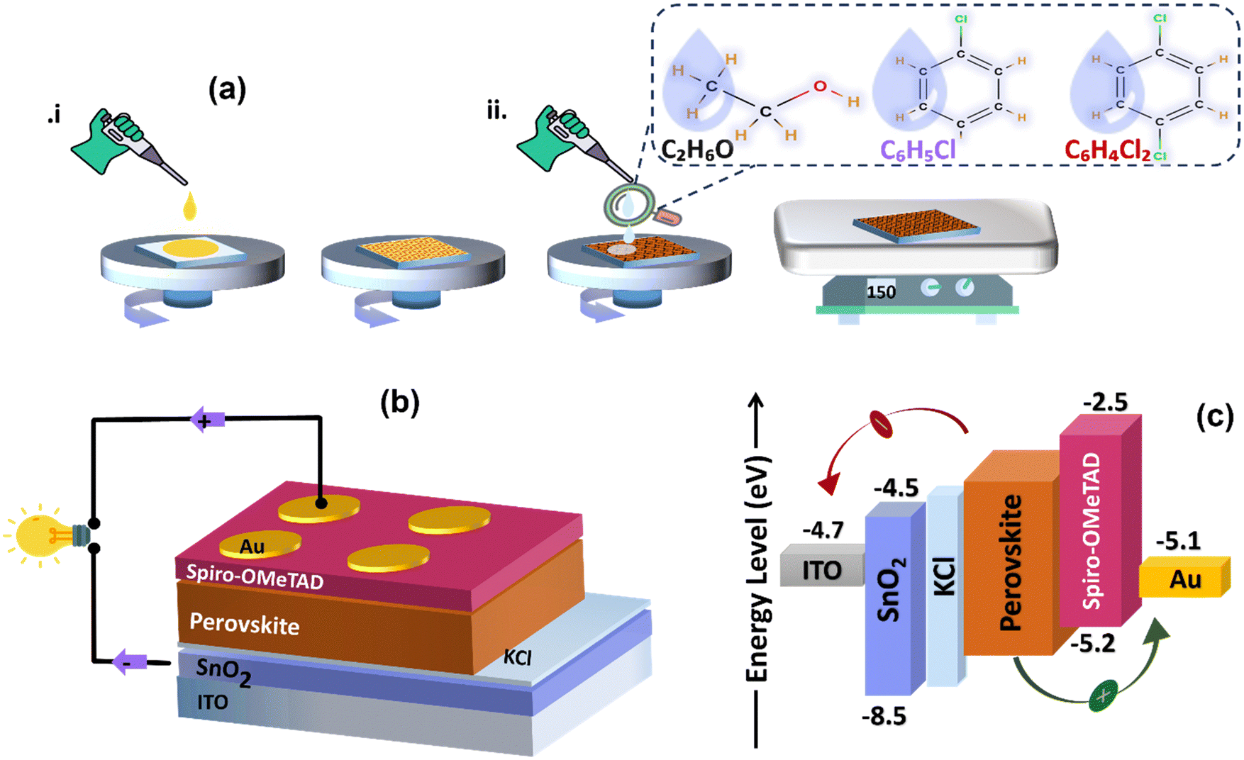 | ||
| Fig. 1 The schematic representation of (a) fabrication process of solution-processed planar heterojunction perovskite solar cells PHJ PSCs by applying different anti-solvents (EtOH, CB, and DCB). (b) The final device architecture of PHJ PSCs. (c) Energy bands alignment between electrodes, charge transport layers, and halide perovskites facilitate efficient electron injection into SnO2/KCl and hole injection into spiro-OMeTAD layers. | ||
To attain high-efficiency perovskite solar cells, control of the crystallization and growth of tightly packed perovskite film microstructures is imperative. This is particularly crucial due to the observed shrinkage and porosity of the perovskite film during one-step CH3NH3PbI3−xClx deposition, leading to large pinhole formation (∼5 μm).29 In this study, we used a formamidinium (FA)-based perovskite solution in ambient to investigate the crystalline microstructure under three distinct anti-solvent treatments (absolute EtOH, CB, and DCB). The perovskite thin films are obtained through a two-step spin coating process. We initially spin cast the perovskite precursor solution at 4000 rpm, followed by a second spin combined with solvent dripping at 5000 rpm and annealing to complete crystallization.
Fig. 2(a–c) displays the SEM images of three distinct perovskite thin films on glass/ITO under ambient conditions and treated with pure EtOH, CB, and DCB anti-solvents, respectively. The perovskite grain size and film smoothness are not the primary determinants of the overall device performance. Fig. 2(a) exhibits the microstructure of the perovskite film treated with pure EtOH. The measured average grain size is around 0.87 μm, with a smooth surface exhibiting an average roughness of 5.9 nm, as shown in Fig. 2(d and e). Despite the smooth surface and relatively large grain sizes, pinholes are observed between the grains, and a significant gap is evident around the grain boundaries in various areas of the SEM image, depicted by the broken yellow circles. The presence of pinholes in the perovskite films could significantly impede charge extraction, decreasing the short circuit current (Jsc) and overall PCE.28 The perovskite thin films treated with CB anti-solvent show a slightly different microstructure than films treated with EtOH, with better surface coverage without pinholes. Fig. 2(b) shows that the average grain size measures approximately 0.48 μm, with a roughness of 9.3 nm. The SEM image also reveals that the perovskite thin film does not show a fully continuous film morphology compared to the DCB samples. Remarkably, employing pure DCB results in a densely packed perovskite thin film devoid of evident pinholes and gaps at grain boundaries, in contrast to previous observations made for DCB-treated single cation perovskite thin film fabricated in a controlled environment.27 Additionally, the SEM cross-sectional images in Fig. S1 (ESI†) revealed that DCB-treated PSCs exhibit better substrate/perovskite thin film contact formation without pronounced gaps between the substrate/perovskite interface compared to EtOH- and CB-treated PSCs. The average grain size for the perovskite active layer treated with DCB is approximately 0.65 μm, with a roughness of around 10.2 nm. All anti-solvent treated perovskite thin films exhibit an average thickness of around 650 nm, as shown in Fig. 2(f).
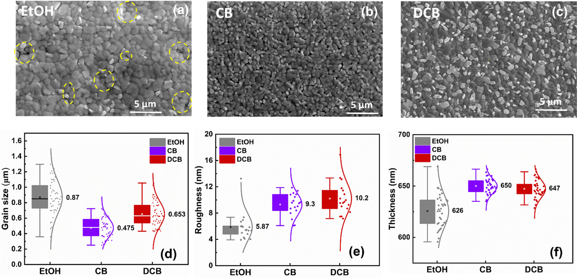 | ||
| Fig. 2 SEM images of the perovskite layers deposited on an ITO substrate using different solvent treatments: (a) EtOH, (b) CB, and (c) DCB. Frequency distribution plots illustrating the (d) grain sizes, (e) roughness of perovskite thin films, and (f) thickness of perovskite thin films treated with the different anti-solvents. | ||
Fig. 3(a) displays XRD patterns of thin films treated with EtOH, CB, and DCB anti-solvents and post-annealed at 70 °C for 5 minutes and 150 °C for 10 minutes. All XRD patterns are characterized by peaks positioned at 2θ ≈ 14.1° and 28.3°, indicating the formation of (110) and (220) crystal planes of the α-FAPbI3 phase attributed to desirable perovskite thin films.30 The DCB anti-solvent treated perovskite thin film exhibits more intense diffraction peaks at the known angles attributed to the tetragonal crystalline perovskite, which are 2θ = 14.08° and 2θ = 28.32°. These peaks confirm the successful formation of a highly crystalline perovskite structure. The presence of residual PbI2 peak is apparent in all three films. There are conflicting reports about the role of residual PbI2 in the performance of PSCs.31,32 Some studies show that lower PbI2 content enables devices to perform better, while others have found that excess PbI2 results in the best-performing PSCs.32–34 However, the presence of more PbI2 is known to catalyze the degradation of perovskite films.35
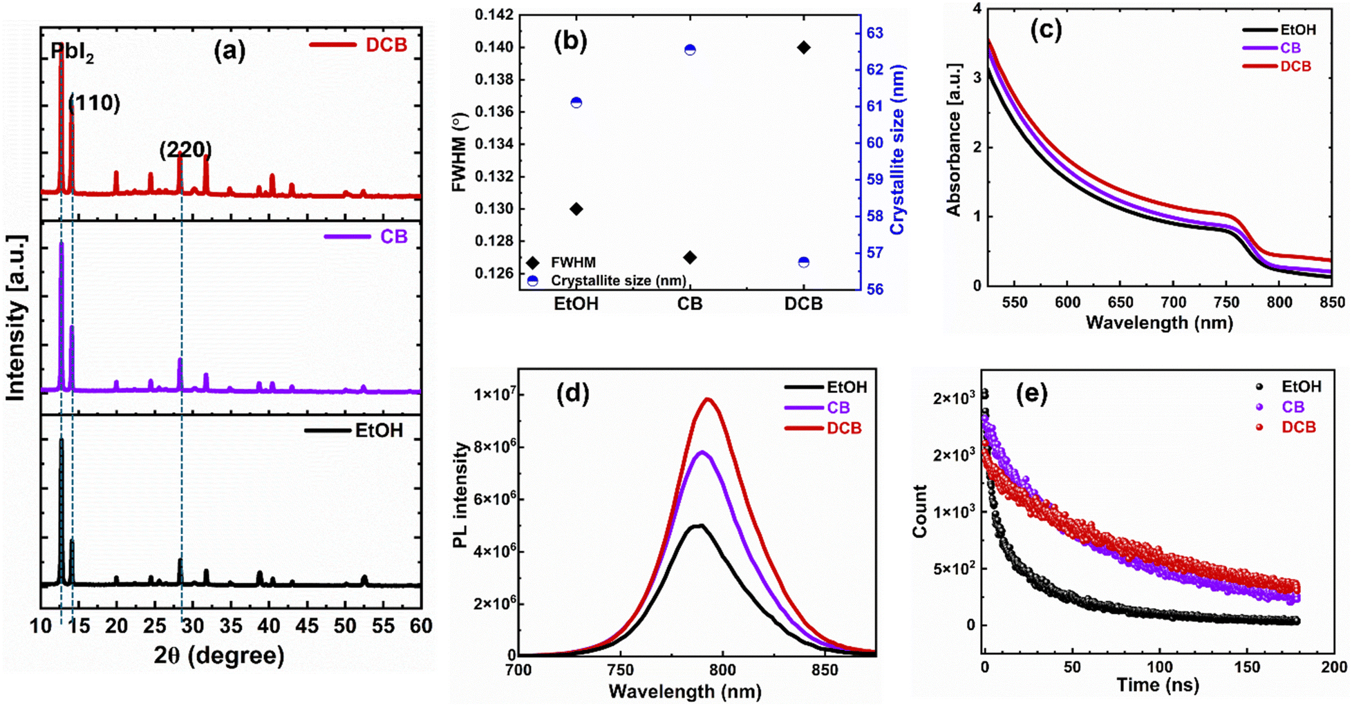 | ||
| Fig. 3 (a) XRD pattern of the perovskite thin films on ITO substrates corresponding to each anti-solvent treatment. (b) Plot showing the calculated full width at half maximum (FWHM) and crystallite size values at 2θ = 14.1°. (c) UV-Vis-NIR absorption spectra of the thin films. (d) Steady-state photoluminescence (PL) spectra of the perovskite thin films deposited on glass substrates. (e) Time-resolved photoluminescence (TRPL) profiles of the perovskite thin films deposited on glass substrates. | ||
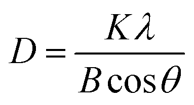
We also measured the coherence length, often assumed to be equivalent to the average crystallite size, of the (110) reflection of the anti-solvent-treated perovskite thin films using Scherrer's eqn (1).
 | (1) |
To elucidate the optical properties and charge transport dynamics of PSCs, we conducted absorption, photoluminescence (PL), and time-resolved PL (TRPL) measurements on thin films deposited onto glass substrates. In Fig. 3(c), we show the similar absorption spectra of the three films. The optical bandgap exhibits almost no change (1.55 eV for EtOH and CB and 1.54 eV for DCB). Therefore, the anti-solvent treatment does not affect the absorption of the perovskite thin films. As shown in Fig. 3(d), the intense PL intensity from DCB-treated perovskite films indicates that anti-solvent exposure helps form a higher quality film and effectively suppresses non-radiative charge carrier recombination.36Fig. 3(e) shows the normalized TRPL for the perovskite coated with various antisolvent treatments. The carrier lifetimes from TRPL profiles, determined via bi-exponential fittings, are presented in the ESI,† Table S1. In general, the slow decay component (τ1) is attributed to non-radiative recombination from surface defects and traps at the grain boundaries, and τ2 is the fast decay component, linked to the quenching of charge carriers at the interface and the bulk.29,30 The TRPL analysis reveals an improvement in carrier lifetime τ2 for the DCB- and CB-treated films of 110 ns and 80 ns, respectively, in contrast to the EtOH-based perovskite films with a carrier lifetime of 35 ns. The extended carrier lifetime is due to higher crystallinity and suppression of defects in the DCB-treated perovskite films.36 Thus, the microstructural crystallinity and morphology, PL, and TRPL characteristics of the DCB-treated ambient perovskite films point to better performance over CB-treated, especially EtOH-treated devices.
We then fabricated planar PSCs with the following structure: glass/ITO/SnO2/KCl/perovskite/spiro-OMeTAD/Au. A comprehensive description of the procedure, from perovskite solution preparation to device fabrication steps, is provided in the Experimental section. We measured the J–V characteristics test under AM 1.5G irradiation to determine the performance of the devices. From the findings shown in Fig. 4(a), DCB-treated PSCs are generally the most efficient of the three types of devices at 20.1% for highest performing solar cells, followed by CB-treated devices at 18.2% and then EtOH-treated devices at 17.2% with device area of 0.092 cm2. Though all three devices yielded similar short circuit current (Jsc) of 24.5 mA cm−2, 24.4 mA cm−2, and 24.9 mA cm−2, respectively, for EtOH-, CB-, and DCB-treated PSCs, DCB-based PSC exhibit the highest open circuit voltage (Voc) of 1.131 V (compared to 1.049 V for CB-based PSC and 1.062 V for EtOH-based PSC) and the highest fill factor (FF) at 71.1% compared to 70.9% and 66.2% respectively for CB- and EtOH-based devices. Table 1 shows the best values and similar trends for the average values of PCEs obtained from the statistics of the reproducible figures of merit (from PCE, Jsc, Voc, and FF), as depicted in Fig. 4(b–e). We ascribe the better performance of DCB-treated PSCs to the overall effect of DCB anti-solvent in ambient on the perovskite films. The exposure to DCB leads to densely packed perovskite crystallites in the thin film that are devoid of pinholes and gaps at grain boundaries, reasonable average grain sizes, higher film quality, effective suppression of nonradiative charge carrier recombination, and long charge carrier lifetimes, when compared to CB-treated PSCs that show intermediate performance and EtOH anti-solvent-treated PSCs that exhibit the lowest, yet still substantial, performance. The 17.2% efficiency from green solvent-treated devices is reasonable compared to chlorinated solvent-based PSCs (approximately 1% less than CB and 3% less than DCB), their microstructure and short charge carrier lifetimes indicate the presence of defects and recombination that could impede stability (see early stability study in Fig. S3, ESI†). Indeed, the EtOH-treated PSCs showed more loss in PCE in our stability study under continuous illumination, followed by the DCB-treated PSCs, and CB-treated PSCs as the most stable devices. Also, the presence of more PbI2, as shown in Fig. 3a, can catalyze device degradation. A deeper investigation of the long-term stability of DCB-based perovskite solar cells is required to fully assess the role of PbI2 in these films. A detailed stability study is beyond the scope of this work and will constitute future work.
 | ||
| Fig. 4 (a) Current density–voltage (J–V) characteristics of the champion devices treated using EtOH, CB, and DCB antisolvents a with device area of 0.092 cm2. (b) Frequency distribution plot of the planar heterojunction perovskite solar cells (PSCs) treated with corresponding anti-solvents (b) power conversion efficiency (PCE) showing DCB-treated PSCs averaging efficiencies 11% and 16% higher than those of CB- and EtOH-treated PSCs respectively, (c) short-circuit current density, (Jsc) with marginally similar average currents between DCB- and CB-treated PSCs (d) open-circuit voltage (Voc) showing DCB-treated PSCs averaging values of 3–5% higher than those of CB- and EtOH-treated PSCs, (e) fill-factor (FF) showing DCB-treated PSCs averaging values 4% and 11% higher than those of CB- and EtOH-treated PSCs respectively. | ||
| Anti-solvent treatment | J sc (mA cm−2) | V oc (V) | FF (%) | Best PCE (%) | Avg. PCE ± SD (%) |
|---|---|---|---|---|---|
| EtOH | 24.5 | 1.062 | 66.2 | 17.2 | 16.3 ± 0.5 |
| CB | 24.4 | 1.049 | 70.9 | 18.2 | 17.0 ± 0.9 |
| DCB | 24.9 | 1.131 | 71.1 | 20.1 | 18.9 ± 0.6 |
To gain more insight into the differences caused by the three antisolvent treatments of the perovskite layers on the devices, we examine charge carrier transport and dynamics in all three systems. We measured and analyzed the transient photocurrent (TPC) and transient photovoltage (TPV) of the PSCs using the Fluxim AG Paios set-up. Fig. 5(a) shows the TPC for the various PSCs. The TPC decay times obtained after fitting are 1.17 μs, 1.12 μs, and 0.98 μs for EtOH, CB, and DCB-treated devices, respectively. The decay time decreased to 0.98 μs for DCB, suggesting an excellent charge carrier extraction process in the device, explaining their better performance compared to CB- and EtOH-based PSCs.33 In Fig. 5(b), we plotted the TPV data measured under open-circuit conditions. The graph displays two distinct time regimes: the first, associated with trap-assisted recombination, and the second, linked to carrier recombination at the interface.37,38 The carrier recombination lifetimes obtained after fitting the TPV data are 46.82 μs for EtOH-treated, 48.62 μs for CB-treated, and 63.09 μs for DCB-treated PSCs, suggesting similar lifetimes for both EtOH and CB-treated devices. These results indicate that nonradiative charge recombination was minimized in the DCB-based solar cells compared to the other two. Particularly, recombination is substantially minimized for DCB-treated devices, which translates to higher Voc and FF, and thus, better performance.36,38 Furthermore, we measured dark currents for the three devices to corroborate the reduced charge recombination lifetime observed for the DCB-treated devices. The DCB-based PSCs consistently exhibit slightly lower leakage currents than the other two, as shown in Fig. 5(c). Such lower leakage currents suggest lower background carrier density and better diode behavior of the PSCs.39
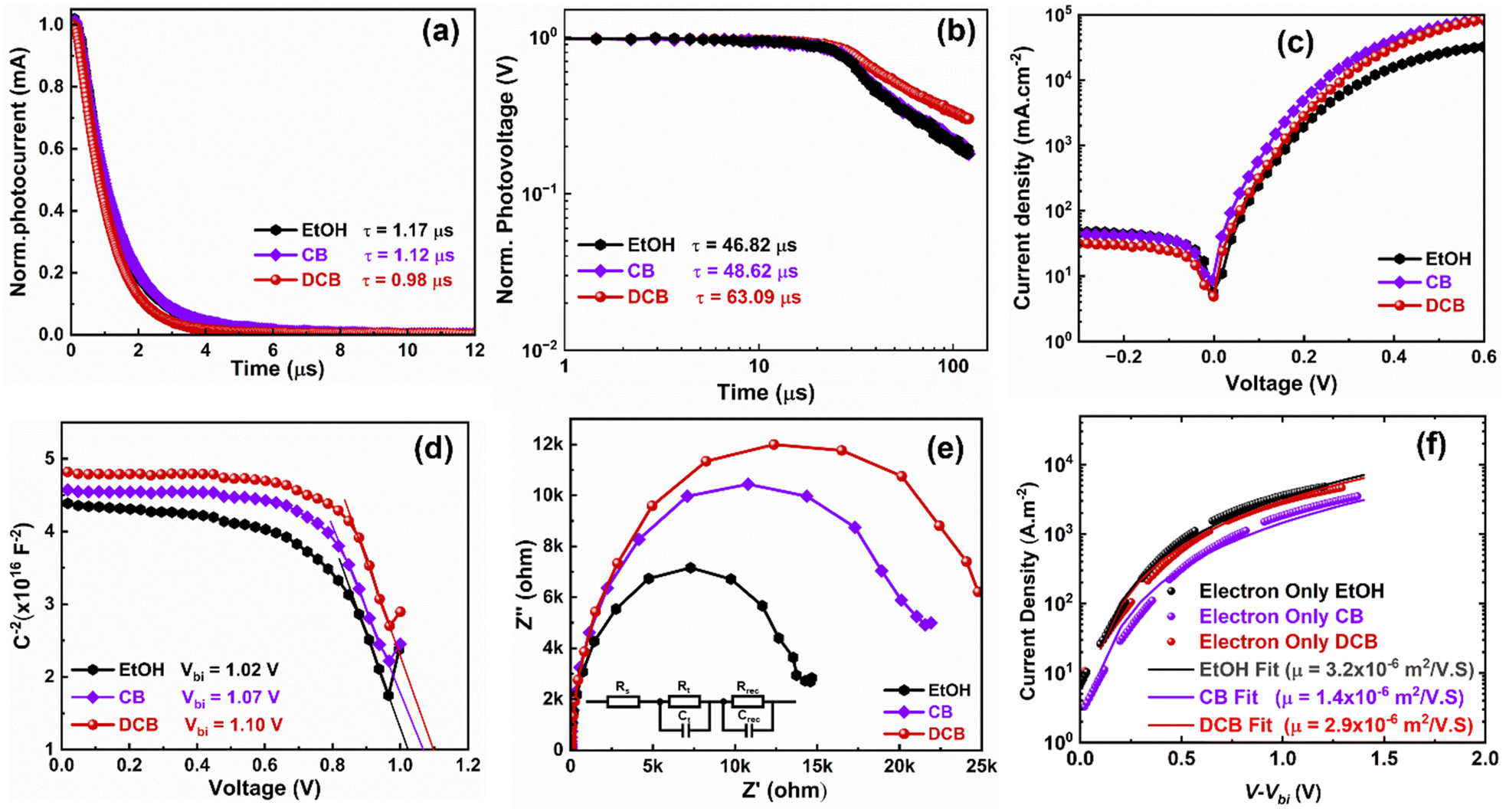 | ||
| Fig. 5 (a) Transient photovoltaic current (TPC), and (b) transient photovoltage (TPV) plots of the PHJ PSCs treated using EtOH, CB, and DCB anti-solvents. (c) Dark J–V curves of PHJ PSCs using corresponding anti-solvent treatments. (d) Capacitance–voltage plot measured at room temperature at a fixed frequency of 10 kHz for each solvent treatment. (e) Nyquist plots of three different PHJ PSCs with the inset showing the equivalent circuit for fitting the impedance spectroscopy (EIS) data (insert: equivalent circuit for fitting of data). (f) The fitted J–V curve to the modified Mott–Gurney equation. | ||
Furthermore, a Mott–Schottky analysis is performed to better understand the improved Voc. Fig. 5(d) shows the capacitance–voltage plot measured at room temperature at a fixed frequency of 10 kHz. The built-in potential (Vbi) of 1.10 V is obtained for DCB-treated devices compared to 1.02 V and 1.07 V for EtOH and CB-treated devices, respectively. These results again corroborate the enhanced Voc observed for DCB-treated PSCs compared to CB- and EtOH-treated PSCs.39,40 A similar deduction on the effectively suppressed charge recombination in the DCB-treated devices can be drawn from the impedance spectroscopy (EIS) measurement depicted in the Nyquist plots for the three devices in Fig. 5(e). To fit the EIS data, an R–R||C–R||C equivalent circuit (shown as an insert in Fig. 5(e)) is used, which includes the series resistance Rs, the charge transfer resistance Rt, and the interfacial charge recombination resistance Rrec. The arc at a low-frequency regime is associated with Rrec.41,42 It has been observed that DCB suppresses the charge recombination, resulting in improved device performance. Likewise, electron-only single carrier devices were made with the following structure: glass/ITO/SnO2/perovskite/PC61BM/Ag. The fitted JV to the modified Mott–Gurney equation16 is displayed in Fig. 5(f) for the EtOH-, CB-, and DCB-treated devices. The extracted mobilities for DCB- and EtOH-treated devices are around 3 × 10⁻⁶ m2 V−1 s−1, and that of the CB-treated device is around 1.4 × 10⁻⁶ m2 V−1 s−1. This may partly explain the slightly better Jsc of their PSCs compared to CB-treated devices. However, this may not have readily translated into (i) efficient charge extraction as shown earlier through measurements of charge carrier decay time via TPC, (ii) balanced charge carriers, leading to loss in the FF, or (iii) minimized losses through charge carrier recombination as alluded earlier from SEM images and TPV with the lowest charge carrier recombination lifetime for the EtOH-based devices. Therefore, our experimental and device physics analyses are evidence of the improved performance of PSCs treated with DCB anti-solvent.
Additionally, we used high-resolution X-ray photoelectron spectroscopy (XPS) to characterize the chemical states (the location of the maximum valence band in relation to the Fermi level energy Ef) of the all-ambient solution-processed perovskite thin films deposited on ITO/SnO2 substrates. The XPS survey spectra acquired from the perovskite thin films presented in Fig. 6(a) show peaks at 138.5 ± 0.2 eV, associated with the Pb 4f7/2 core level indicative of Pb–X (X = I, Cl) bonds. Additional core level peaks such as C 1s, N 1s, and I 3d5/2 were observed at 288.4 ± 0.1 eV, 400.8 ± 0.1 eV, and 619.2 ± 0.2 eV, respectively, attributed to the FA1−xCsxPbI3 perovskite.43,44 Fig. S2 (ESI†) displays the individual carbon species attributed to the C 1s core level, and Fig. 6 depicts the Pb 4f7/2 core levels (b, c, d). As specified in Table S2 (ESI†), a reduction of Pb2+ to metallic lead (Pb0) is observed. This reduction is attributed to a multi-origin degradation mechanism of the perovskite thin films, as discussed by Bechu et al.43
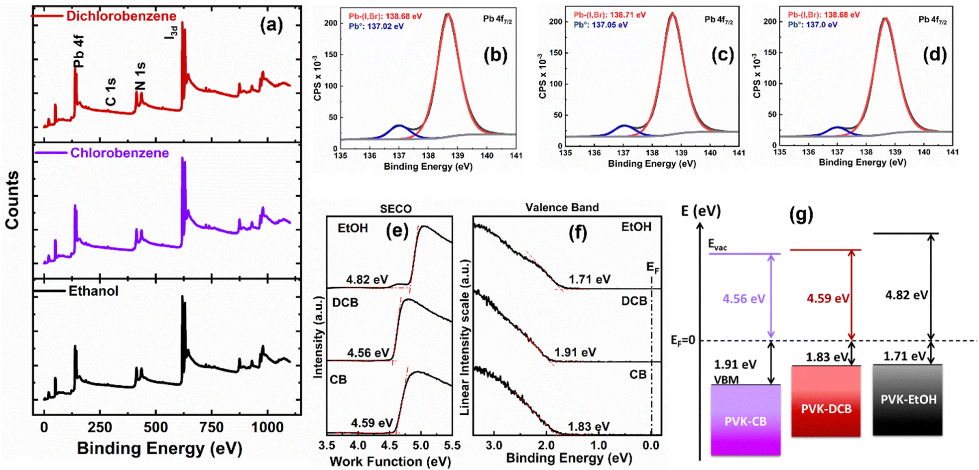 | ||
| Fig. 6 (a) X-ray photoelectron spectroscopy (XPS) spectra showing Pb 4f, C 1s, N 1s, and I 3d core levels of FAPbI3 after anti-solvent treatments. XPS spectra of the Pb 4f7/2 core level attributed to FAPbI3 of the (b) EtOH, (c) CB, and (d) DCB antisolvents treated perovskite thin films. UPS spectra of the perovskite thin films with (e) SECO showing the work function value (ϕ) and (f) valence band spectra of the treated-perovskite thin films. (g) The energy-level scheme of the treated-perovskite thin films. | ||
To assess the band alignment between the perovskite layer and charge transport layers, we conducted ultraviolet photoelectron spectroscopy (UPS) measurements on the FA1−xCsxPbI3 perovskite thin films on ITO substrates. The work function (ϕ) of the thin films was determined using the secondary electron cut-off (SECO) method, as shown in Fig. 6(e). The ϕ values are 4.59 eV, 4.56 eV, and 4.82 eV for the DCB-, CB-, and EtOH-treated films, respectively. It is observed that the work function of the EtOH-treated film is higher than that of both the DCB and CB-treated films. The valence band maxima (VBM) were determined based on the spectrum's onset, as shown in Fig. 6(f). For our thin films, the EVBM is measured at 1.83 eV for DCB-treated samples, 1.91 eV, and 1.71 eV for CB and EtOH-treated samples, respectively. Variations in the EVBM values among our samples can be attributed to the distinct functional groups present in the applied anti-solvents on the perovskite thin films. The presence of OH groups in the EtOH anti-solvent likely induces a surface dipole,45 thereby elevating the work function in EtOH-treated samples compared to the chlorinated ones. We also presented an energy-level alignment scheme in Fig. 6(g) for the perovskite layers, and the calculated values are shown in Table S3 (ESI†). The DCB-treated sample exhibited the smallest EVB value, facilitating hole extraction. This suggests a lower energy barrier for hole-carrier collection at the interface of the perovskite thin films and spiro-OMeTAD. It is known that lower energy barriers are linked to reduced surface recombination rates, potentially increasing Voc.45,46 Indeed, these findings support the charge transport dynamics explained using device physics.
Conclusions
We have demonstrated the fabrication of perovskite thin films under ambient conditions by treating films using an anti-solvent, either one of two chlorinated anti-solvents or a green solvent. We show that dichlorobenzene performs well as an anti-solvent, similarly to chlorobenzene, and improves the crystal quality of halide perovskite thin films and their optoelectronic properties. Additionally, using a green solvent, ethanol, results in a promising device efficiency of 17.2%. Surface defects are reduced with DCB treatment, which leads to an enhanced solar cell performance with a PCE of 20.1%. The higher efficiency of DCB-based solar cells is attributed to suppressed non-radiative recombination of devices and lower leakage current. Overall, this work reveals that DCB solvent treatment facilitates the ambient processing of efficient perovskite solar cells.Experimental methods
Materials
Except otherwise specified, most materials and solvents were supplied by Sigma-Aldrich. In addition, lead(II) iodide (PbI2), lead(II) chloride (PbCl2), cesium iodide (CsI), and potassium chloride (KCl) were purchased from TCI America, while formamidinium iodide (FAI) and FK209 were supplied by Greatcell solar materials and spiro-OMeTAD from Ossila. Absolute ethanol, chlorobenzene, and dichlorobenzene were purchased from VWR.Formulation of perovskite precursor solution
To prepare the perovskite precursor solution, the commercially available FAI, CsI, and PbI2 were dissolved in a mixed solvent of N,N-dimethylformamide (DMF), and N-methyl-2-pyrrolidone (NMP). A double cation perovskite of formulation Cs0.17FA0.83PbI3 was prepared in the mixed solvents. The precursor solution was then stirred for about 5 hours at 700 rpm to obtain a yellowish transparent perovskite precursor solution. Before spin coating, the perovskite solution was filtered with a 0.45 μm PTFE filter (Ossila).Device fabrication
All perovskite layers were deposited under the same ambient environmental conditions (RH ≈ 15–35%), and anti-solvents were applied during the second step of the spin coating process.Device and thin film characterization
To examine the morphology and microstructural evolution of perovskite thin films, we employed field-emission scanning electron microscopy (FE-SEM) with a Verios G4 XHR SEM (Thermo Scientific). For the X-ray diffraction (XRD) analysis of the films, a Malvern Panalytical Empyrean IV, PIXcel 3D, and 1Der detector was utilized to study crystallinity and ascertain the phase composition of the perovskite films. Time-resolved photoluminescence (TRPL) and steady-state photoluminescence (PL) spectra were obtained from the FLS1000 photoluminescence spectrometer (Edinburgh Instrument, FLS1000). The J–V characteristics were measured using a Keithley 4200 source meter for the PSCs in the dark and under simulated 100 mW cm−2 AM 1.5 G solar radiation. This radiation was generated by a 450 W xenon lamp (Oriel Sol 2A Class ABA), calibrated with a reference silicon cell covered by KG5 filtered glass. The short-term stability curves of the PSCs were recorded by collecting their J–V response under 100 mW cm−2 irradiance generated by a steady-state LED lamp (Ossila Solar Simulator Class AAA). Fluxim AG Paios system with white LED light was used to carry out the transient photocurrent (TPC), transient photovoltage (TPV), capacitance–voltage (Mott–Schottky analysis), and electrochemical impedance spectroscopy (EIS) measurements.The XPS experiments were conducted with a VersaProbe III instrument from Physical Electronics, outfitted with a concentric hemispherical analyzer beside a monochromatic Al Kα X-ray source (hν = 1486.6 eV). Charge neutralization was omitted in the procedure. Calibration of the binding energy axis involved the use of sputter-cleaned Cu (Cu 2p3/2 = 932.62 eV, Cu 3p3/2 = 75.1 eV) and Au foils (Au 4f7/2 = 83.96 eV). Measurements were conducted at a takeoff angle of 45° relative to the sample surface plane, resulting in a typical sampling depth of 3–6 nm (where 95% of the signal originated from this depth or shallower). Peaks were calibrated with reference to the CHx band in the carbon 1 s spectra at 284.8 eV. The analysis size was approximately 200 μm in diameter. Quantification was achieved using instrumental relative sensitivity factors (RSFs), which consider the X-ray cross-section and inelastic mean free path of electrons. Major elements (>5 atom%) on homogeneous samples typically exhibit less than 3% standard deviations, whereas minor elements may show significantly higher deviations.
Conflicts of interest
The authors declare no conflict of interest.Acknowledgements
The authors thank Jeffery Shallenberger from the materials characterization lab (MCL) of The Pennsylvania State University for his assistance in acquiring the XPS data and part of the analysis. The authors acknowledge the help of Dr Kavyasheree Keremane of The Pennsylvania State University with early lab sample preparation. We acknowledge Dr Bangzhi Liu from the nanofabrication lab of The Pennsylvania State University for the help with the SEM cross-sectional images. I. M. Asuo and E. D. Gomez acknowledge support from the Office of Naval Research under Award N00014-19-1-2453. N. Y. Doumon acknowledges support from the Materials Research Institute (MRI) and the Institute of Energy and the Environment (IEE) of The Pennsylvania State University, University Park.References
- Y. Cheng, Q. Wei, Z. Ye, X. Zhang, P. Ji, N. Wang, L. Zan, F. Fu and S. Frank Liu, Sol. RRL, 2022, 6, 2200418 CrossRef CAS.
- G. Li, Z. Wang, Y. Wang, Z. Yang, P. Dong, Y. Feng, Y. Jiang, S.-P. Feng, G. Zhou, J.-M. Liu and J. Gao, Small, 2023, 19, 2301323 CrossRef CAS PubMed.
- J. Jiao, C. Yang, Z. Wang, C. Yan and C. Fang, Results Eng., 2023, 18, 101158 CrossRef CAS.
- K. Lin, J. Xing, L. N. Quan, F. P. G. de Arquer, X. Gong, J. Lu, L. Xie, W. Zhao, D. Zhang, C. Yan, W. Li, X. Liu, Y. Lu, J. Kirman, E. H. Sargent, Q. Xiong and Z. Wei, Nature, 2018, 562, 245–248 CrossRef CAS PubMed.
- X. Guo, I. M. Asuo, A. Pignolet, R. Nechache and S. G. Cloutier, Opt. Mater. Express, 2022, 12, 153–165 CrossRef CAS.
- J. Moon, Y. Mehta, K. Gundogdu, F. So and Q. Gu, Adv. Mater., 2023, 2211284 CrossRef PubMed.
- Y. Zhao, X. Yin, P. Li, Z. Ren, Z. Gu, Y. Zhang and Y. Song, Nano-Micro Lett., 2023, 15, 187 CrossRef CAS PubMed.
- I. M. Asuo, D. Gedamu, I. Ka, L. F. Gerlein, F.-X. Fortier, A. Pignolet, S. G. Cloutier and R. Nechache, Nano Energy, 2018, 51, 324–332 CrossRef CAS.
- R.-J. Jin, Y.-H. Lou, L. Huang, K.-L. Wang, C.-H. Chen, J. Chen, F. Hu and Z.-K. Wang, Adv. Mater., 2024, 2313154 CrossRef PubMed.
- A. Kojima, K. Teshima, Y. Shirai and T. Miyasaka, J. Am. Chem. Soc., 2009, 131, 6050–6051 CrossRef CAS PubMed.
- M. A. Green, E. D. Dunlop, J. Hohl-Ebinger, M. Yoshita, N. Kopidakis and X. Hao, Prog. Photovoltaics Res. Appl., 2021, 29, 657–667 CrossRef.
- X. Cao, G. Su, L. Hao, J. Zhou, Q. Zeng, X. He and J. Wei, J. Mater. Chem. C, 2024, 12, 1631–1639 RSC.
- J. Sun, F. Li, J. Yuan and W. Ma, Small Methods, 2021, 5, 2100046 CrossRef CAS PubMed.
- X. Yuan, R. Li, Z. Xiong, P. Li, G. O. Odunmbaku, K. Sun, Y. Deng and S. Chen, Adv. Funct. Mater., 2023, 33, 2215096 CrossRef CAS.
- X. Li, D. Bi, C. Yi, J.-D. Décoppet, J. Luo, S. M. Zakeeruddin, A. Hagfeldt and M. Grätzel, Science, 2016, 353, 58–62 CrossRef CAS PubMed.
- I. M. Asuo, D. Gedamu, N. Y. Doumon, I. Ka, A. Pignolet, S. G. Cloutier and R. Nechache, Mater. Adv., 2020, 1, 1866–1876 RSC.
- K. Geistert, S. Ternes, D. B. Ritzer and U. W. Paetzold, ACS Appl. Mater. Interfaces, 2023, 15, 52519–52529 CAS.
- W. Zhang, T. Zhang, L. Qin, S.-Z. Kang, Y. Zhao and X. Li, Chem. Eng. J., 2024, 479, 147838 CrossRef CAS.
- N. J. Jeon, J. H. Noh, Y. C. Kim, W. S. Yang, S. Ryu and S. I. Seok, Nat. Mater., 2014, 13, 897–903 CrossRef CAS PubMed.
- O. A. Khaleel and D. S. Ahmed, Opt. Mater., 2022, 126, 112148 CrossRef CAS.
- J. Li, R. Yang, L. Que, Y. Wang, F. Wang, J. Wu and S. Li, J. Mater. Res., 2019, 34, 2416–2424 CrossRef CAS.
- D. Gedamu, I. M. Asuo, D. Benetti, M. Basti, I. Ka, S. G. Cloutier, F. Rosei and R. Nechache, Sci. Rep., 2018, 8, 12885 CrossRef PubMed.
- H. Yang, H. Wang, J. Zhang, J. Chang and C. Zhang, Coatings, 2019, 9, 766 CrossRef CAS.
- K.-M. Lee, C.-J. Lin, B.-Y. Liou, S.-M. Yu, C.-C. Hsu, V. Suryanarayanan and M.-C. Wu, Sol. Energy Mater. Sol. Cells, 2017, 172, 368–375 CrossRef CAS.
- D. Prochowicz, M. M. Tavakoli, A. Solanki, T. W. Goh, K. Pandey, T. C. Sum, M. Saliba and P. Yadav, J. Mater. Chem. A, 2018, 6, 14307–14314 RSC.
- Y. Chen, W. Wu, R. Ma and C. Wang, J. Mol. Struct., 2019, 1175, 632–637 CrossRef CAS.
- G.-H. Kim, J. Jeong, H. Jang, J. W. Kim and J. Y. Kim, Thin Solid Films, 2018, 661, 122–127 CrossRef CAS.
- A. D. Taylor, Q. Sun, K. P. Goetz, Q. An, T. Schramm, Y. Hofstetter, M. Litterst, F. Paulus and Y. Vaynzof, Nat. Commun., 2021, 12, 1878 CrossRef CAS PubMed.
- X. Gong, M. Li, X.-B. Shi, H. Ma, Z.-K. Wang and L.-S. Liao, Adv. Funct. Mater., 2015, 25, 6671–6678 CrossRef CAS.
- W. Luo, J. Zhong, L. Zhang, Y. Peng, J. Lu, M. Xu and Z. Ku, Mater. Sci. Semicond. Process., 2023, 164, 107603 CrossRef CAS.
- A. D. Taylor, Q. Sun, K. P. Goetz, Q. An, T. Schramm, Y. Hofstetter, M. Litterst, F. Paulus and Y. Vaynzof, Nat. Commun., 2021, 12, 1878 CrossRef CAS PubMed.
- M. Saliba, T. Matsui, J.-Y. Seo, K. Domanski, J.-P. Correa-Baena, M. K. Nazeeruddin, S. M. Zakeeruddin, W. Tress, A. Abate, A. Hagfeldt and M. Grätzel, Energy Environ. Sci., 2016, 9, 1989–1997 RSC.
- Q. Chen, H. Zhou, T.-B. Song, S. Luo, Z. Hong, H.-S. Duan, L. Dou, Y. Liu and Y. Yang, Nano Lett., 2014, 14, 4158–4163 CrossRef CAS PubMed.
- T. J. Jacobsson, J. P. Correa-Baena, E. Halvani Anaraki, B. Philippe, S. D. Stranks, M. E. Bouduban, W. Tress, K. Schenk, J. Teuscher, J. E. Moser, H. Rensmo and A. Hagfeldt, Unreacted PbI2 as a Double-Edged Sword for Enhancing the Performance of Perovskite Solar Cells, J. Am. Chem. Soc., 2016, 138(32), 10331–10343 CrossRef CAS PubMed.
- P. Fassl, V. Lami, A. Bausch, Z. Wang, M. T. Klug, H. J. Snaith and Y. Vaynzof, Energy Environ. Sci., 2018, 11, 3380–3391 RSC.
- M. Kim, G.-H. Kim, T. K. Lee, I. W. Choi, H. W. Choi, Y. Jo, Y. J. Yoon, J. W. Kim, J. Lee, D. Huh, H. Lee, S. K. Kwak, J. Y. Kim and D. S. Kim, Joule, 2019, 3, 2179–2192 CrossRef CAS.
- X. Zhang, S. Eurelings, A. Bracesco, W. Song, S. Lenaers, W. Van Gompel, A. Krishna, T. Aernouts, L. Lutsen, D. Vanderzande, M. Creatore, Y. Zhan, Y. Kuang and J. Poortmans, ACS Appl. Mater. Interfaces, 2023, 15, 46803–46811 CrossRef CAS PubMed.
- H. Bi, Y. Fujiwara, G. Kapil, D. Tavgeniene, Z. Zhang, L. Wang, C. Ding, S. R. Sahamir, A. K. Baranwal, Y. Sanehira, K. Takeshi, G. Shi, T. Bessho, H. Segawa, S. Grigalevicius, Q. Shen and S. Hayase, Adv. Funct. Mater., 2023, 33, 2300089 CrossRef CAS.
- L. Chen, E. Kinsa Tekelenburg, K. Gahlot, M. Pitaro, J. Xi, A. Lasorsa, G. Feraco, L. Protesescu, P. C. A. van der Wel, G. Portale, P. Rudolf, C. J. Brabec and M. Antonietta Loi, Energy Environ. Sci., 2023, 16, 5315–5324 RSC.
- S. Shao, Y. Cui, H. Duim, X. Qiu, J. Dong, G. H. ten Brink, G. Portale, R. C. Chiechi, S. Zhang, J. Hou and M. A. Loi, Adv. Mater., 2018, 30, 1803703 CrossRef PubMed.
- S. Yuan, T. Zhang, H. Chen, Y. Ji, Y. Hao, H. Zheng, Y. Wang, Z. David Chen, L. Chen and S. Li, Chem. Eng. J., 2022, 433, 133227 CrossRef CAS.
- H. Zheng, X. Peng, T. Chen, T. Zhang, S. Yuan, L. Wang, F. Qian, J. Huang, X. Liu, Z. David Chen, Y. Zhang and S. Li, J. Energy Chem., 2023, 84, 354–362 CrossRef CAS.
- S. Béchu, M. Ralaiarisoa, A. Etcheberry and P. Schulz, Adv. Energy Mater., 2020, 10, 1904007 CrossRef.
- A. Bensekhria, I. M. Asuo, I. Ka, R. Nechache and F. Rosei, Improved Performance of Air-Processed Perovskite Solar Cells via the Combination of Chlorine Precursors and Potassium Thiocyanate, ACS Appl. Mater. Interfaces, 2023, 15(48), 56413–56423 CrossRef CAS PubMed.
- J. Tirado, M. Vásquez-Montoya, C. Roldán-Carmona, M. Ralaiarisoa, N. Koch, M. K. Nazeeruddin and F. Jaramillo, ACS Appl. Energy Mater., 2019, 2, 4890–4899 CrossRef CAS.
- K. Taek Cho, S. Paek, G. Grancini, C. Roldán-Carmona, P. Gao, Y. Lee and M. Khaja Nazeeruddin, Energy Environ. Sci., 2017, 10, 621–627 RSC.
- N. Y. Doumon, M. V. Dryzhov, F. V. Houard, V. M. Le Corre, A. Rahimi Chatri, P. Christodoulis and L. J. A. Koster, ACS Appl. Mater. Interfaces, 2019, 11, 8310–8318 CrossRef CAS PubMed.
- P. N. Murgatroyd, J. Phys. D: Appl. Phys., 1970, 3, 308 Search PubMed.
Footnote |
| † Electronic supplementary information (ESI) available. See DOI: https://doi.org/10.1039/d4tc01305k |
| This journal is © The Royal Society of Chemistry 2024 |