
 Open Access Article
 This Open Access Article is licensed under a
 Creative Commons Attribution 3.0 Unported Licence
Ambipolar charge-trapping in self-assembled nanostructures of a supramolecular miktoarm star-shaped copolymer with a zinc phthalocyanine core†
Xinhao
Zhong
ab,
Debdatta
Panigrahi
 c,
Ryoma
Hayakawa
c,
Yutaka
Wakayama
*c,
Koji
Harano
d,
Masayuki
Takeuchi
*ab and
Junko
Aimi
*a
c,
Ryoma
Hayakawa
c,
Yutaka
Wakayama
*c,
Koji
Harano
d,
Masayuki
Takeuchi
*ab and
Junko
Aimi
*a
aResearch Center for Macromolecules and Biomaterials, National Institute for Materials Science (NIMS), 1-2-1 Sengen, Tsukuba, Ibaraki 305-0047, Japan. E-mail: AIMI.Junko@nims.go.jp; TAKEUCHI.Masayuki@nims.go.jp
bDepartment of Materials Science and Engineering, Faculty of Pure & Applied Sciences, University of Tsukuba, 1-1-1 Tennodai, Tsukuba, Ibaraki 305-8577, Japan
cResearch Center for Materials Nanoarchitectonics (MANA), NIMS, 1-1 Namiki, Tsukuba, Ibaraki 305-0044, Japan. E-mail: WAKAYAMA.Yutaka@nims.go.jp
dCenter for Basic Research on Materials, NIMS, 1-1 Namiki, Tsukuba, Ibaraki 305-0044, Japan
First published on 21st May 2024
Abstract
Nonvolatile organic field-effect transistor (OFET) memories have attracted considerable attention owing to their potential applications in flexible and wearable electronic devices. The novel design of a charge-trapping material based on supramolecular miktoarm star copolymers (μ-stars) consisting of star-shaped polystyrene with a zinc phthalocyanine core (ZnPcPS4) and a pyridyl end-functionalized polymer (py-polymer) has been studied to explore the influence of self-assembled morphology on the final device performances. Supramolecular μ-stars containing the ZnPc core showed distinctive phase-separated nanostructures in the films that were different from typical polymer blends. The OFET memory devices embedded with supramolecular μ-stars exhibited ambipolar charge-trapping behavior with photoresponsive characteristics, resulting in a wide memory window (47 V) with a high on/off current ratio (>107) for a long period of time (>104 s). Furthermore, the charge-trapping properties of the polymer memory layer were studied using Kelvin probe force microscopy (KPFM), revealing enhanced charge-trapping capabilities attributed to nanoscale phase separation in the supramolecular μ-stars. This study provides the design and concept of charge-trapping materials for next-generation high-performance OFET memory devices.
Introduction
Nonvolatile organic field-effect transistor (OFET) memory devices, designed to retain data post-power disruption, hold significant promise for integration into flexible and wearable organic electronic devices, such as cost-effective wireless tags and biosensors.1–3 OFET memory involves an architecture wherein a memory layer is inserted between the charge-transporting layer and the gate electrodes. Various materials, including ferroelectric materials,4–6 polymer electrets,7,8 and nano-floating gates,9–11 have been employed as memory layers in OFET devices. Memory characteristics originate from field-effect modulation by spontaneous polarization in ferroelectrics or charge trapping in dielectrics.12,13 To introduce these memory layers into OFETs while maintaning transistor performance, polymer-based memory materials offer advantages in terms of ease of fabrication and application to flexible devices.The memory performance of the device is assessed based on the memory window, which denotes the shift in the threshold voltage (ΔVth) caused by trapped charges or polarized dipoles within the memory material. A large memory window facilitates easier differentiation between the “0” and “1” digital states at the reading voltage. Additionally, controllable memory shifts are advantageous for achieving multilevel data storage, thus further enhancing the memory capacity without enlarging the device size.14,15 The magnitude of the memory window is influenced by the density of charge-trapping sites and the intensity of the applied electric field in the tunneling layer, potentially affecting the retention ability due to charge leakage from insufficient insulation of the adjacent charge-trapping sites.16 Extensive research has demonstrated that morphological control of the charge-trapping layer is crucial for optimizing the memory performance.12,16–18 Notably, microstructures formed by the self-assembly of block copolymers have been studied for preparing well-defined charge-trapping layers.19–22 For instance, Leong et al. demonstrated in situ synthesis of Au nanoparticles within self-assembled poly(styrene-b-poly(4-vinyl pyridine)) block copolymers to prepare well-defined nano-floating gates. The phase morphology of the block copolymer affected the loading density of the nanoparticles, thereby controlling the memory window.23 Chiu et al. reported OFET memory utilizing sugar-based block copolymers containing maltoheptaose (MH), where the orientation of microdomains influenced the memory window.24 Ambipolar charge-trapping was also achieved by introducing 1-aminopyrene into the polymer microdomains via supramolecular interactions. Yang et al. recently introduced a pyrene-functionalized block copolymer for photoresponsive memory.25 Phototransistor memory, which operates via light irradiation rather than voltage application, has been gaining importance because of its low energy consumption and rapid data processing.26–30 Phototransistor memory has recently been applied to artificial synaptic memory that mimics the human brain.31 This uses optical signals to mimic the synapses responsible for information transmission between nerve cells, where memory depends on the intensity or frequency of external stimuli. Such integration of nonvolatile data storage and processing functions into a single OFET device has potential applications for neuromorphic devices which are attracting attention in the field of artificial intelligence and deep learning.32,33
We recently developed OFET memory devices using a star-shaped polymer with a metallophthalocyanine (MPc) core as a nano-floating gate (Fig. 1(a)).34–36 The MPc core acts as a charge-trapping site, whereas the surrounding polymer arms hinder charge leakage to achieve nonvolatile characteristics. Taking advantage of polymer-based nano-floating gates, the MPc-cored star polymer was easily fabricated into logic circuits such as inverters, demonstrating multilevel or reconfigurable logic-in-memory applications.37,38 In this polymer nano-floating gate system, the memory window of the OFET memory has been expanded by increasing the density of the MPc core in the polymer film, which was controlled by the length of the polymer arms using precision polymer synthesis.35 On the other hand, increasing the core density shortened the memory retention time and decreased the charge carrier mobility of the organic semiconductor. The shorter retention time was attributed to potential charge leakage arising from insufficient insulation of the adjacent MPc core charge-trapping sites. The decrease in the charge carrier mobility was linked to the crystal growth of the organic semiconductor, which was influenced by the structure of the polymer thin film. The phase morphology of the memory material appears to be critical to the memory performance, particularly the memory window and charge retention properties.
 | ||
| Fig. 1 Chemical structures of ZnPcPS4 (a) and py-polymers (b). (c) Preparation of a supramolecular miktoarm star-shaped copolymer with a ZnPc core through coordination interaction. | ||
In this study, an OFET memory with ambipolar charge-trapping characteristics is demonstrated. Supramolecular miktoarm star copolymers (μ-stars) composed of star-shaped polystyrene with a zinc phthalocyanine core (ZnPcPS4) and pyridyl end-functionalized polymers (py-polymer) as memory materials (Fig. 1(b)) have been utilized.39 Asymmetric polymers, such as block copolymers and miktoarm star copolymers, are known to show unique phase behavior via self-assembly.40–42 By using metal–ligand coordination, AB4-type supramolecular μ-stars with a functional core were facilely prepared without a tedious synthetic procedure (Fig. 1(c)). We expect that the morphology of the asymmetric star-shaped polymers may influence the device performance in OFET memory. The thin-film morphology and charge-trapping behavior of supramolecular μ-stars were investigated by atomic force microscopy (AFM), transmission electron microscopy (TEM), and Kelvin probe force microscopy (KPFM). The polymer films containing supramolecular μ-stars showed a unique morphology characteristic of microphase separation, which is different from normal blend polymers. Polymer films containing the ZnPc core were further fabricated for OFET memory, showing ambipolar charge-trapping behavior by electronic and photo-assisted programming/erasing operations. This OFET memory possessed long memory retention capability, which was further enhanced by the microphase separation of μ-stars. The relationship between the phase morphology and charge-trapping behavior was investigated.
Experimental section
Materials
Commercial chemicals purchased from Aldrich Chemical Co., Inc., TCI, Wako Chemicals, FUJIFILM Wako Pure Chemical Corporation, and Kanto Chemicals were used without further purification, unless noted otherwise.Measurements
Atomic force microscopy (AFM) was performed under ambient conditions using Bruker Dimension Icon and Dimension IconIR. Surface morphology imaging was conducted in the ScanAsyst mode using a silicon cantilever (ScanAsyst-Air). Nanoscale infrared (IR) spectroscopy was conducted in the IIR tapping mode using a gold-coated silicon cantilever (PR-UM-TNIR-D-10). X-ray diffraction (XRD) measurements were performed using a Bruker D8 Discover with a Cu Kα X-ray source. Transmission electron microscopy (TEM), high-angle annular dark-field (HAADF) scanning transmission electron microscopy (STEM), and energy-dispersive spectroscopy (EDS) analyses were conducted using a Thermo Fisher Scientific Talos F200X G2 equipped with an EDS detector (Super-X G2) at an acceleration voltage of 80 kV. The specimens were prepared by scooping a thin film of polymer in water using a TEM copper grid with a lacy carbon support (NS-C15, Okenshoji Co., Ltd). The probe current for HAADF-STEM microscopy and EDS mapping was set to 1.6 nA. EDS analysis was xperformed using Velox software (Thermo Fisher Scientific) with a single three-parameter Bethe-Heitler function as the background correction parameter. Kelvin probe force microscopy (KPFM) measurements were completed using a scanning probe microscope (Shimadzu, SPM-9700HT) under ambient conditions. A conductive silicon tip coated with a Pt–Ir alloy was used as the cantilever (Nanoworld, EFM). The voltage applied to the cantilever was controlled by using a source measurement unit (Keysight Technology, B2912A).Device fabrication and measurement
OFET memory devices with a C8-BTBT organic semiconductor layer were prepared on a highly doped p+-Si (001) substrate with a 200 nm thick SiO2 layer. First, the substrates were cleaned via sequential ultrasonication in acetone and ethanol. Subsequently, a thin layer of the polymer was spin-coated onto the SiO2 surface. The organic semiconductor C8-BTBT was vacuum-deposited onto the polymer film using shadow masks. The top-contact gold electrodes were thermally deposited as the source and drain electrodes using another shadow mask to complete the transistor fabrication process. Light-assisted memory operations were performed using a xenon lamp (Asahi Spectra, MAX-303) with ultraviolet (UV) light (250–380 nm) and LED lamps (730 and 365 nm, Asahi Spectra, CL-1501).Electrical measurements were performed using an Agilent B1500A semiconductor parameter analyzer under ambient conditions. The charge carrier mobility (μ) and threshold voltage (Vth) values were estimated from the slope and intercept of the linear plot of the square root of the drain-to-source current (I1/2ds) vs. the gate voltage (Vg) in the saturation regime using the following equation:
 | (1) |
The relationships between the capacitances of the device (Ctot), SiO2 wafer (CSiO2), and polymers (Cpoly) and the polymer dielectric constant (ε) are defined as follows:
 | (2) |
 | (3) |
Results and discussion
Morphology of a supramolecular miktoarm star copolymer
The supramolecular μ-stars were formed by blending ZnPcPS4 and pyridine-tethered polymers (py-polymer) in organic solvents. In the previous study, we prepared three types of py-polymers, poly(methyl methacrylate) (pyPMMA), poly(vinyl acetate) (pyPVAc), and poly(N-vinyl carbazole) (pyPVK), by reversible addition–fragmentation chain transfer (RAFT) polymerization (Fig. 1(b)).39 The average molecular weights (Mn) of each py-polymer were 13.9 kg mol−1 for pyPMMA, 16.1 kg mol−1 for pyPVAc, and 13.0 kg mol−1 for pyPVK, respectively. They have similar Mn to that of ZnPcPS4 (14.2 kg mol−1) (Table S1, ESI†). The metal–ligand coordination between ZnPcPS4 and three types of py-polymers in solution has been confirmed by spectral studies by means of UV-vis absorption and 1H-NMR measurements.39 To investigate the phase morphologies of polymer films containing supramolecular μ-stars, polymer films were prepared by spin-coating each polymer mixture (5 mg mL−1) in a mass ratio of 1![[thin space (1/6-em)]](https://www.rsc.org/images/entities/char_2009.gif) :1. Notably, the Mn of the py-tethered polymers was similar to that of ZnPcPS4, which is considered to have a molar ratio of approximately 1:1, corresponding to the 1:1 complexation observed between the ZnPc core and the pyridyl end-group. Another set of polymer films containing py-polymers and star-shaped polystyrene without a ZnPc core (PS4) was prepared. The Mn of PS4 is 16 kg mol−1, which is similar to that of ZnPcPS4. Binary polymer blends of PS/PMMA, PS/PVAc, and PS/PVK are known to exhibit various phase-separated structures due to the strong segregation between immiscible polymers.43,44 Therefore, the differences in film morphology with and without the ZnPc core were investigated to ascertain the influence of the supramolecular interactions on the polymer blend.
:1. Notably, the Mn of the py-tethered polymers was similar to that of ZnPcPS4, which is considered to have a molar ratio of approximately 1:1, corresponding to the 1:1 complexation observed between the ZnPc core and the pyridyl end-group. Another set of polymer films containing py-polymers and star-shaped polystyrene without a ZnPc core (PS4) was prepared. The Mn of PS4 is 16 kg mol−1, which is similar to that of ZnPcPS4. Binary polymer blends of PS/PMMA, PS/PVAc, and PS/PVK are known to exhibit various phase-separated structures due to the strong segregation between immiscible polymers.43,44 Therefore, the differences in film morphology with and without the ZnPc core were investigated to ascertain the influence of the supramolecular interactions on the polymer blend.
The surface morphologies of the polymer blend films were analyzed by AFM. Fig. 2(a) shows the AFM height image of a film spin-coated from a toluene solution of a mixture of ZnPcPS4 and pyPMMA (ZnPcPS4/pyPMMA). The film exhibited a distinct phase separation with a domain size of approximately 50 nm. The phase-separated morphology was analyzed using AFM combined with nanoscale infrared (IR) spectroscopy (AFM-IR). The AFM image was monitored at selected absorption wavenumbers of 1730 and 1492 cm−1, corresponding to the carbonyl stretching band of PMMA and the benzene C![[double bond, length as m-dash]](https://www.rsc.org/images/entities/char_e001.gif) C stretching vibrations of PS, respectively. As shown in Fig. 2(b), the relatively higher and brighter parts in the AFM image were characterized as the PMMA domain, whereas the other domains were dominated by PS. In contrast, the blend polymer film containing PS4 and pyPMMA exhibited irregular and micrometer-sized phase separation in the AFM height image (Fig. S1, ESI†). The root-mean-square (RMS) surface roughness (Rq) of the blended polymer film of PS4 and pyPMMA was estimated to be 1.36 nm, which was larger than that of the ZnPcPS4/pyPMMA film (0.49 nm). The smoother film surfaces and smaller domain sizes of phase separation implied the influence of coordination interaction between ZnPc and the pyridyl end-group in the supramolecular μ-star.
C stretching vibrations of PS, respectively. As shown in Fig. 2(b), the relatively higher and brighter parts in the AFM image were characterized as the PMMA domain, whereas the other domains were dominated by PS. In contrast, the blend polymer film containing PS4 and pyPMMA exhibited irregular and micrometer-sized phase separation in the AFM height image (Fig. S1, ESI†). The root-mean-square (RMS) surface roughness (Rq) of the blended polymer film of PS4 and pyPMMA was estimated to be 1.36 nm, which was larger than that of the ZnPcPS4/pyPMMA film (0.49 nm). The smoother film surfaces and smaller domain sizes of phase separation implied the influence of coordination interaction between ZnPc and the pyridyl end-group in the supramolecular μ-star.
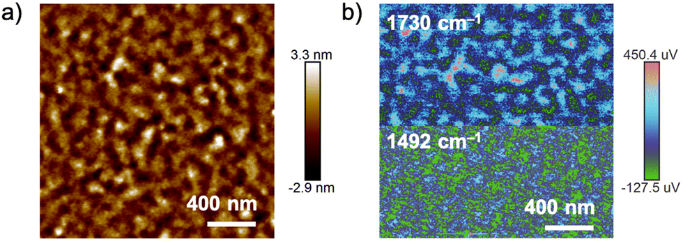 | ||
| Fig. 2 (a) AFM height image of a blended film of ZnPcPS4/pyPMMA. (b) AFM-IR image of a blended film of ZnPcPS4/pyPMMA by monitoring at 1730 cm−1 (top) and 1492 cm−1 (bottom). | ||
The film morphology of the supramolecular μ-star was further investigated by TEM. A 1 wt% toluene solution of ZnPcPS4/pyPMMA was dropped onto the water surface to form a thin film and a portion of the film was scooped onto a TEM grid with a carbon support layer. A contrast between the phase-separated PS and PMMA domains was observed in the bright-field TEM images of the unstained samples (Fig. S2, ESI†). Fig. 3(a) shows a HAADF-STEM image of the supramolecular μ-star film, exhibiting clear phase-separated images with a domain size of 20–50 nm. Elemental mapping of the film using STEM-EDS revealed that the brighter regions of the HAADF-STEM image had a higher carbon content than the darker regions, whereas the darker regions overlapped with oxygen-rich domains (Fig. 3(b)). This result indicates that the bright region corresponds to the PS domain, whereas the other domain is dominated by PMMA. Notably, the elemental mapping of Zn in ZnPcPS4 overlapped with the carbon-rich domains and showed a bright contrast in the HAADF-STEM image owing to the presence of heavy atoms (Fig. S3, ESI†). The film morphology observed by TEM was similar to that observed in the aforementioned AFM images, confirming that the ZnPcPS4/pyPMMA films exhibited phase-separated nanodomains. The coordination interaction between the ZnPc core in ZnPcPS4 and the pyridyl end group of pyPMMA might connect the boundaries between incompatible polymers, reducing the interfacial tension to exhibit microphase separation like that of block copolymers rather than macrophase separation, which is often observed in normal polymer blends. In other words, the supramolecular complexes (μ-stars) in the polymer blend act as a compatibilizer, providing nanosized phase-separated morphology and reducing surface roughness.
 | ||
| Fig. 3 (a) HAADF-STEM image and (b) EDS elemental mapping image of carbon (blue) and oxygen (red) for the ZnPcPS4/pyPMMA film. | ||
Similarly, the surface morphologies of other supramolecular μ-stars (ZnPcPS4/pyPVAc and ZnPcPS4/pyPVK blends) spin-coated from dichloromethane solution were also analyzed by AFM (Fig. 4). A polymer film containing ZnPcPS4 and pyPVAc exhibited distinct phase separation (Fig. 4(a)), whereas the film from a mixture of PS4 and pyPVAc displayed a droplet-like morphology owing to the strong phase segregation between PVAc and PS (Fig. 4(c)). The surface roughness Rq of ZnPcPS4/pyPVAc was 6.28 nm, and it was much smoother than the PS4/pyPVAc blended film (30.4 nm). A similar trend was observed for the blended films containing PS and PVK. The polymer containing ZnPcPS4/pyPVK showed nanoscale phase separation (Fig. 4(b)), whereas stronger phase segregation and a relatively rough surface were observed in the PS4/PVK blended film (Fig. 4(d)). These results support the abovementioned assumption that metal–ligand coordination between the ZnPc core and pyridyl end-groups in the polymers influences the bulk film morphology of the blended polymers. Such nanostructures from microphase separation are often observed in block copolymers or μ-stars; however, the preparation of various asymmetric polymers is normally difficult due to tedious synthetic procedures. In this study, phase-separated nanostructures of polymer films composed of various polymer blend combinations were successfully obtained by exploiting supramolecular interactions.
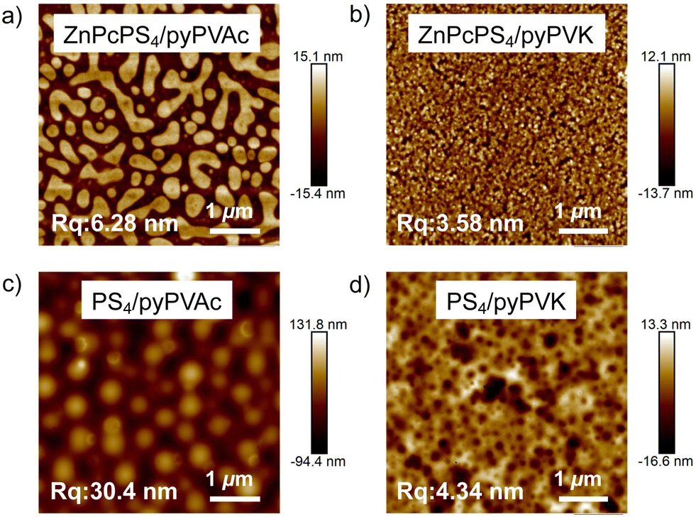 | ||
| Fig. 4 AFM height images of blended films of (a) ZnPcPS4/pyPVAc, (b) ZnPcPS4/pyPVK, (c) PS4/pyPVAc, and (d) PS4/pyPVK. | ||
Characteristics of OFET memory using the supramolecular μ-star
The unique phase-separated morphology of the supramolecular μ-star with the ZnPc core was then utilized in the memory layer of an OFET memory device. To develop the OFET memory, a ZnPcPS4/pyPMMA film was chosen that formed a relatively flat surface, allowing ideal crystal growth of the organic semiconductor. A 2 wt% toluene solution of ZnPcPS4/pyPMMA in a 1:1 mass ratio was spin-coated on a Si wafer with 200 nm SiO2, followed by vacuum deposition of 2,7-dioctyl[1]benzothieno[3,2-b][1]benzothiophene (C8-BTBT)45 and gold electrodes. The device architecture with a bottom-gate top-contact configuration is shown in Fig. 5(a). The thicknesses of the memory layer and the C8-BTBT layer estimated by X-ray reflectivity measurements were 27.0 and 14.9 nm, respectively. OFET memory devices embedded with ZnPcPS4 or pyPMMA memory layers were also prepared for comparison.
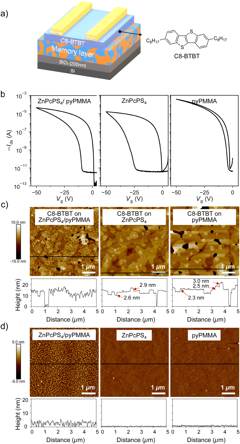 | ||
| Fig. 5 (a) Device architecture of C8-BTBT-based OFET memory with a polymer memory layer. (b) Transfer characteristics of OFET memory devices with memory layers of ZnPcPS4/pyPMMA (left), ZnPcPS4 (middle), and pyPMMA (right). AFM height images and cross-sectional profiles of (c) C8-BTBT and (d) polymer layers. | ||
The transfer and output characteristics of the fabricated OFET devices are shown in Fig. 5(b) and Fig. S4 (ESI†), respectively. A typical p-type accumulation mode with sweep direction dependence was observed for the fabricated OFET devices. The estimated charge carrier mobility (μ), on/off current ratio (Ion/Ioff), and initial threshold voltage (Vth) are listed in Table S2 (ESI†). The charge carrier mobility of the OFET with the ZnPcPS4/pyPMMA layer was estimated to be 0.43 cm2 V−1 s−1, which is slightly higher than that of the ZnPcPS4-embedded device of 0.33 cm2 V−1 s−1. This result indicated that the phase-separated morphology of the underlying supramolecular μ-star did not disturb the charge transport properties in the C8-BTBT semiconductor layer. However, the morphology of the C8-BTBT film on the ZnPcPS4/pyPMMA surface appeared to be influenced by the underlying polymer, as shown in Fig. 5(c). The surface morphology of C8-BTBT on the ZnPcPS4 or pyPMMA homopolymers showed islands with a smooth top surface on a continuous layer, which appeared to follow the Stranski–Krastanov growth modes. The cross-sectional profiles of C8-BTBT on ZnPcPS4 revealed that the step height of the islands was approximately 2.9 nm in the top layer and 2.6 nm on the second layer, with an underlying layer approximately 10 nm below (Fig. 5(c), middle). The long axis of C8-BTBT was approximately 3 nm,46 suggesting that the molecule was aligned in a standing-up orientation normal to the substrate.47 Meanwhile, the surface morphology of C8-BTBT on ZnPcPS4/pyPMMA showed a similar layer and islands, but a relatively rough surface (Fig. 5(c), left). This indicates that the crystal growth of C8-BTBT occurs similarly to the flat PS and PMMA surfaces, but it is in accordance with the initial surface roughness of the phase-separated morphology (Fig. 5(d)). Indeed, the out-of-plane X-ray diffraction (XRD) profile of C8-BTBT on the blend or homopolymer showed almost the same patterns as those of the crystalline structures (Fig. S5, ESI†). The sharp peak at 2θ = 3.1°, originating from the (001) Bragg reflection, was estimated to have a d-spacing of 2.8 nm. Taken together with the AFM results, the C8-BTBT films formed highly ordered layer-by-layer phases, even on the phase-separated surface of ZnPcPS4/pyPMMA, resulting in a comparable charge carrier mobility in OFET devices.
In the transfer curve of the memory devices embedded with ZnPc-containing polymers, a clear hysteresis was observed between forward and backward sweeps for Vg between +5 and −50 V at a fixed drain voltage (Vd) of −50 V (Fig. 5(b), left and middle). This result indicated that the holes accumulated in C8-BTBT were trapped in the memory layer while sweeping to a negative Vg. In contrast, no significant hysteresis was observed in devices with pyPMMA (Fig. 5(b), right). It should also be noted here that the charge carrier mobility values of the OFET devices with ZnPc-containing polymer layers were lower than those with pyPMMA. Since the crystal structure of C8-BTBT on ZnPcPS4 or pyPMMA did not show clear differences in the AFM images, this discrepancy was probably due to charge trapping during sweeping, which could prevent efficient charge migration in the organic semiconductor.35 The magnitude of the hysteresis was maximal for the ZnPcPS4-embedded memory device, which was approximately twice as large as that of the ZnPcPS4/pyPMMA-embedded device. This result was reasonable because the concentration of ZnPc, i.e., the density of the charge-trapping site, was reduced by approximately half in the supramolecular μ-star film.
To quantitatively evaluate the memory performance, programming/erasing operations of the OFET memory devices were conducted by applying a Vg pulse and light irradiation. When a negative gate bias was applied to the ZnPcPS4/pyPMMA-embedded OFET memory (Vg = −60 V for 1 s), the transfer curve shifted toward the negative direction (Fig. 6(a), red line). This process is referred to as programming (hole-trapping), in which the holes accumulated in the C8-BTBT semiconductor layer are transferred to and stored in the memory layer. The average shift of Vth (ΔVth(+)) was 25.4 V for the ZnPcPS4/pyPMMA-embedded device and 31.5 V for the ZnPcPS4-embedded device (Fig. S6, ESI†). The OFET memory with the pyPMMA layer showed a small shift of 5.3 V, confirming that significant charge trapping occurred owing to the presence of the ZnPc core (Fig. S7, ESI†). Interestingly, the erasing process was accomplished by UV light irradiation. When the OFET memory device was exposed to UV light (250–380 nm) with an intensity of 2.5 mW cm−2 for 5 s after the programming process, the transfer curve shifted back to the initial position (Fig. 6(a), purple line). This process is referred to as photo-erasing. By irradiating the device with UV light, a significant number of excitons (electron–hole pairs) can be generated on the semiconducting layer because C8-BTBT exhibits strong absorption in the UV region of the spectrum (Fig. S8, ESI†). Some electrons might effectively neutralize the trapped holes at the interface between the C8-BTBT layer and the underlying memory layer, achieving an erasing process in the absence of an electric field.26,48 Another possible mechanism of photo-erasing is the annihilation of the trapped charges by excitons induced in the memory layer.49,50 However, we found that photo-erasing could be completed by LED light irradiation at 365 nm (Fig. S9a, ESI†), while 730 nm LED light irradiation, corresponding to the absorption of ZnPc, cannot complete this process (Fig. S9b, ESI†). Thus, charge annihilation may be primarily due to the excitons of C8-BTBT, as previously mentioned. Furthermore, when Vg = +60 V was applied for 5 s under UV irradiation, the transfer curve shifted in the positive direction as +21.9 V (Fig. 6(a), blue line). This process is referred to as photo-assisted programming (electron trapping). In this process, the photogenerated excitons were separated by an external electric field and some electrons were trapped in the underlying polymer layer. This resulted in a positive shift in Vth, eventually giving OFET memory devices a large memory window with ambipolar charge-trapping behavior. This photo-assisted programming process was not achieved by the LED light irradiation at 730 nm (Fig. S9b, ESI†). This indicates that excitons generated within the semiconductor triggered the memory programming. The proposed mechanisms of hole trapping, photo-erasing, and photo-assisted electron trapping are illustrated in Fig. 6(b). The positive Vth shift of the ZnPcPS4/pyPMMA-embedded OFET memory device was larger than that of the ZnPcPS4-embedded device. This result suggested that electrons were trapped not only in the ZnPc core but also in the polymer chains and/or interfaces. A similar trend was observed in the OFET memory with a memory layer of phase-separated block copolymer, where charge trapping occurred in the interfaces between the polymer domains.21 Phase separation of the supramolecular μ-star might be favorable for electron trapping, resulting in a comparable memory window of approximately 47.0 V for all operations (Fig. S6, ESI†).
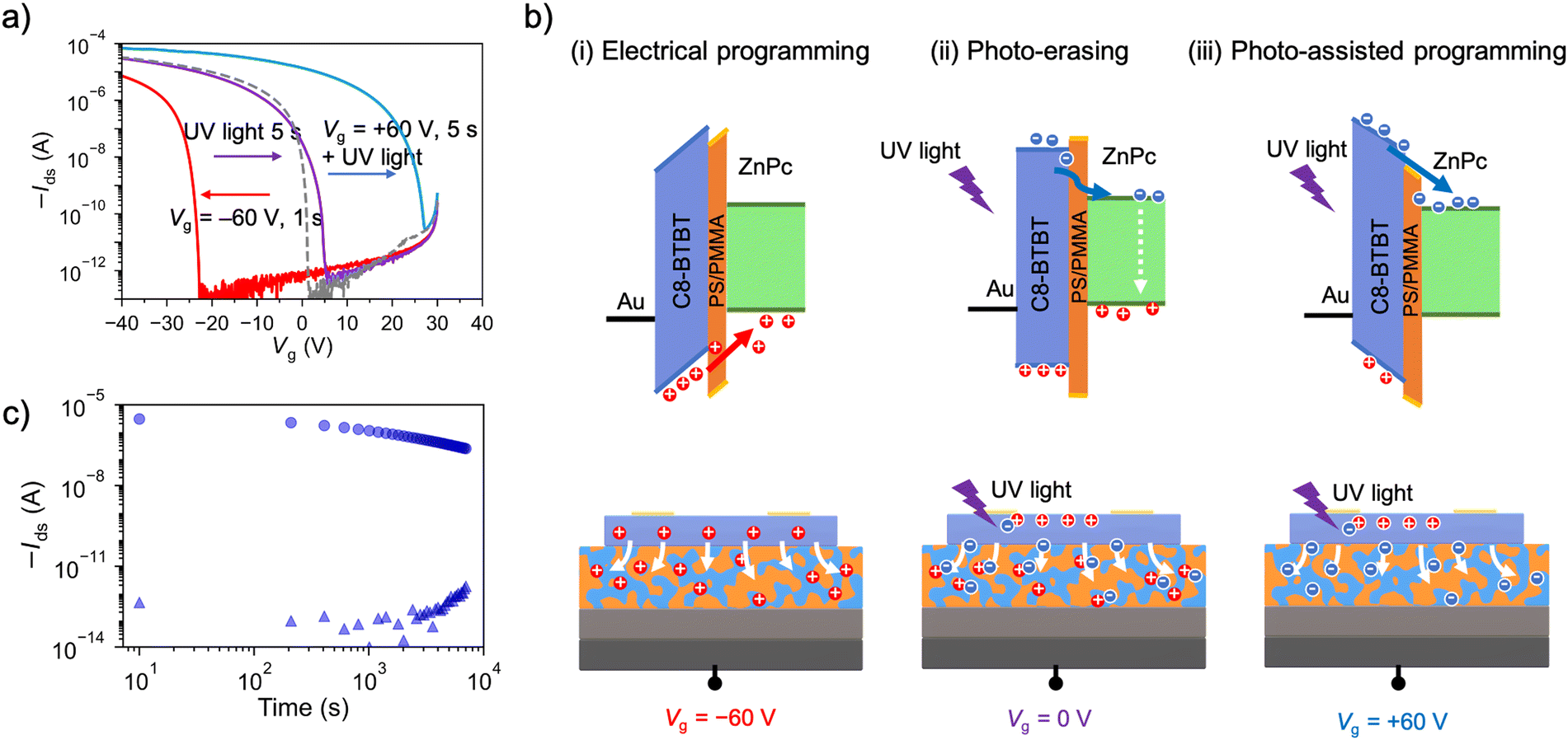 | ||
| Fig. 6 (a) Transfer characteristics of the OFET memory device with a polymer layer of ZnPcPS4/pyPMMA at Vd = −50 V. (b) Schematics and energy-level alignments during the (i) electrical programming operation, (ii) UV-light-assisted erasing operation, and (iii) UV-light-assisted programming operation. (c) Retention time of the Ids monitored at Vg = 0 V and Vd = −10 V after hole-trapping (triangle) and electron-trapping (circle). | ||
The conditions of the photo-assisted programming were also optimized by varying the applied Vg (Fig. S10a, ESI†). When the applied Vg was gradually increased from 0 to +60 V under light irradiation for 5 s, the memory window saturated at Vg = +40 V, indicating that the applied voltage could be reduced by light irradiation. This result also suggested that the drain current can be controlled by applying voltage and/or light, thereby exhibiting potential applications in multilevel data storage (Fig. S10b, ESI†).
The retention time of the OFET memory device after the programming process was evaluated to demonstrate its reliability. As shown in Fig. 6(c), the drain current was monitored at Vg = 0 V under Vd = −10 V after applying Vg = −60 V for 1 s (OFF state) or Vg = +60 V for 5 s under UV light irradiation (ON state). These correspond to hole-trapped and electron-trapped states in OFET memory, respectively. The on/off current ratio remained at 105 after 3 h for the ZnPcPS4/pyPMMA-embedded OFET memory device, indicating the superior charge retention capability of the polymer layer. Notably, ZnPcPS4/pyPMMA showed a longer electron-trapping retention time than the ZnPcPS4 and pyPMMA layers (Fig. S11, ESI†). Considering its large memory window and long charge-retention capability, the phase-separated morphology of ZnPcPS4/pyPMMA was assumed to provide efficient charge trapping and suppress charge leakage. Therefore, the charge-trapping behaviors of the polymer films were investigated.
Charge-trapping properties in polymer memory layers
Charge injection, retention, and diffusion processes in the polymer films were studied using KPFM. The KPFM technique has been widely used to profile the localized electrical properties of films used in electronic devices because it can simultaneously obtain a high-resolution morphology and surface potential.51,52 This technique allows the evaluation of the electrical potential difference,53,54 charge transport and spatial distribution in the semiconductor channel,55–57 work function for nanostructures,58 and charge-trapping and diffusion properties in the dielectric layer.59–61Three types of polymer films, ZnPcPS4, ZnPcPS4/pyPMMA, and pyPMMA, were prepared by spin-coating toluene solutions onto a highly doped n-type silicon wafer with a 300 nm SiO2 layer. Charges were injected into the polymer film by contact with a conductive tip on the polymer surface with an applied voltage bias (Vtip), while the substrate was ground (Fig. 7(a)). As shown in Fig. 7(b), after injecting a positive bias (Vtip = +10 V) for 30 s onto the ZnPcPS4/pyPMMA film, a spot with a relatively positive potential was observed by scanning the surface potential using KPFM. This result indicates that the strong electric field between the tip and polymer surface extracts electrons by tunneling, inducing holes at the specific injection point. In contrast, electron injection was achieved by applying a negative bias of Vtip = −10 V for 30 s by the contact mode in KPFM. Localized charges were visualized by measuring the surface potential; a relatively negative spot was observed in a specific area of the injection point. The line profiles of the potential peaks after injecting holes or electrons into the ZnPcPS4/pyPMMA film are plotted in Fig. 7(c), where the maximum potential peak decreased very slowly via charge diffusion. Note that the first point of the peak potential was approximately 10 min after charge injection owing to the AFM scanning experimental conditions. The peak potential at 10 min after applying a positive bias was 0.62 V and decreased to 0.32 V after 2 h, while the peak potential after a negative bias was −0.51 V at 10 min and remained at −0.32 V after 2.4 h.
 | ||
| Fig. 7 (a) Schematics of charge-injection experiments using KPFM. (b) Surface potential images of the ZnPcPS4/pyPMMA film after applying Vtip = +10 V (top) and −10 V (bottom). (c) Peak potential change after the charge injection. (d) Decays and exponential curve fittings of the peak potentials with time after charge injection into different polymers. (e) Evolution of the full width at half-maximum (FWHM) of potential curves with time for each polymer. | ||
To further investigate the charge retention and diffusion behavior of the polymer film, charge injection experiments were performed on other polymer thin films of ZnPcPS4 and pyPMMA (Fig. S12, ESI†). The peak potential after the same injection experiments of positive charge was 0.62 V for ZnPcPS4, which is a similar value to that of the ZnPcPS4/pyPMMA film. Meanwhile, the pyPMMA film exhibited the peak potential at 0.42 V after charge injection. The higher peak potentials of the ZnPc-containing polymers indicate the efficient charge-trapping capability of the ZnPc cores in the polymer matrix. After applying a negative Vtip, the negative peak potentials were nearly identical across polymers, approximately 0.5 V. Subsequently, the peak potential maps were continuously analyzed every 8 min after injecting charges (hole or electron) into each polymer and the maximum peak potential was plotted over time. The time dependence of the peak potential of the polymer films is shown in Fig. 7(d), representing decay in the number of trapped charges in the polymer films. The plotted potential peak fits well with the exponential curve according to the following equation:
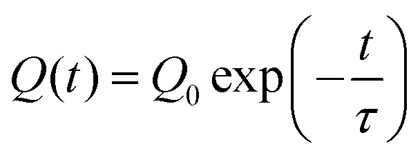 | (4) |
Conclusion
We investigated the effect of the film morphology of charge-trapping polymeric materials on the OFET memory devices using the supramolecular μ-star. The mixtures of ZnPcPS4 and pyridine-terminated polymers (pyPMMA, pyPVAc, pyPVK) formed a supramolecular μ-star, and their spin-coated films exhibited unique microphase separation with smooth film surfaces due to the non-covalent interaction between polymers. The OFET memory device was fabricated using a ZnPcPS4/pyPMMA film as the charge-trapping layer and C8-BTBT as the organic semiconductor. By combining the electric and photo-assisted programming operations, the memory device exhibited ambipolar charge-trapping characteristics. The memory device trapped holes by applying a negative Vg bias, released trapped charges by photoirradiation with UV light, and further trapped electrons when UV light and a positive Vg bias were applied simultaneously. Consequently, the memory device showed a large memory window (∼47 V), a high Ion/Ioff memory ratio (∼107), and long-term charge retention (>104 s). KPFM studies of the polymer films revealed that the ZnPc-containing films had efficient hole-trapping and long retention ability, whereas the ZnPcPS4/pyPMMA films also showed superior retention ability of electrons owing to the surface potential difference at the interfaces of nanostructures of supramolecular μ-stars. Our study suggests that a design strategy for nanostructured charge-trapping materials with functional aromatic molecules can improve the performance of phototransistor memory.Author contributions
J. A. designed the study. X. Z. synthesized the polymers and investigated their morphologies. K. H conducted STEM measurements. All device experiments were conducted by X. Z. with supervision and guidance from D. P., R. H. and Y. W. X. Z. and J. A. wrote the manuscript with input from all the authors. W. Y. and M. T. supervised the project and finalized the manuscript.Conflicts of interest
The authors declare no competing interests.Acknowledgements
We deeply appreciate Dr. Masanobu Naito (NIMS) for the use of the nano-IR instruments. We are also grateful to Ms. Izumi Matsunaga and Ms. Bo Zhou for their technical support in the polymer synthesis and AFM measurements. This study was supported by JSPS KAKENHI (JP21K05220 to J. A., JP21F21052 and JP23H00269 to W. Y., and JP23H04874 to K. H.), a Grant-in-Aid from Izumi Science and Technology Foundation to J. A., and a MEXT “NIMS Molecule and Material Synthesis Platform” program.References
- T. Sekitani, T. Yokota, U. Zschieschang, H. Klauk, S. Bauer, K. Takeuchi, M. Takamiya, T. Sakurai and T. Someya, Science, 2009, 326, 1516–1519 CrossRef CAS PubMed.
- M. L. Hammock, A. Chortos, B. C. Tee, J. B. Tok and Z. Bao, Adv. Mater., 2013, 25, 5997–6038 CrossRef CAS PubMed.
- A. Yamamura, H. Matsui, M. Uno, N. Isahaya, Y. Tanaka, M. Kudo, M. Ito, C. Mitsui, T. Okamoto and J. Takeya, Adv. Electron. Mater., 2017, 3, 1600456 CrossRef.
- J. Hoffman, X. Pan, J. W. Reiner, F. J. Walker, J. P. Han, C. H. Ahn and T. P. Ma, Adv. Mater., 2010, 22, 2957–2961 CrossRef CAS PubMed.
- R. C. Naber, K. Asadi, P. W. Blom, D. M. de Leeuw and B. de Boer, Adv. Mater., 2010, 22, 933–945 CrossRef CAS PubMed.
- J. Y. Park, D. H. Choe, D. H. Lee, G. T. Yu, K. Yang, S. H. Kim, G. H. Park, S. G. Nam, H. J. Lee, S. Jo, B. J. Kuh, D. Ha, Y. Kim, J. Heo and M. H. Park, Adv. Mater., 2023, 35, 2204904 CrossRef CAS PubMed.
- K. J. Baeg, Y. Y. Noh, J. Ghim, S. J. Kang, H. Lee and D. Y. Kim, Adv. Mater., 2006, 18, 3179–3183 CrossRef CAS.
- Y. H. Chou, H. C. Chang, C. L. Liu and W. C. Chen, Polym. Chem., 2015, 6, 341–352 RSC.
- H. C. Chang, C. Lu, C. L. Liu and W. C. Chen, Adv. Mater., 2015, 27, 27–33 CrossRef CAS PubMed.
- C. C. Shih, Y. C. Chiu, W. Y. Lee, J. Y. Chen and W. C. Chen, Adv. Funct. Mater., 2015, 25, 1511–1519 CrossRef CAS.
- L. Van Tho, K. J. Baeg and Y. Y. Noh, Nano Convergence, 2016, 3, 1–7 CrossRef PubMed.
- J. S. Lee, Y. M. Kim, J. H. Kwon, H. Shin, B. H. Sohn and J. Lee, Adv. Mater., 2009, 21, 178–183 CrossRef CAS.
- C. C. Shih, W. Y. Lee and W. C. Chen, Mater. Horiz., 2016, 3, 294–308 RSC.
- Y. L. Guo, C. A. Di, S. H. Ye, X. N. Sun, J. Zheng, Y. G. Wen, W. P. Wu, G. Yu and Y. Q. Liu, Adv. Mater., 2009, 21, 1954–1959 CrossRef CAS.
- J. S. Lee, Y. M. Kim, J. H. Kwon, J. S. Sim, H. Shin, B. H. Sohn and Q. X. Jia, Adv. Mater., 2011, 23, 2064–2068 CrossRef CAS PubMed.
- M. Kang, K. J. Baeg, D. Khim, Y. Y. Noh and D. Y. Kim, Adv. Funct. Mater., 2013, 23, 3503–3512 CrossRef CAS.
- Y. Park, K. J. Baeg and C. Kim, ACS Appl. Mater. Interfaces, 2019, 11, 8327–8336 CrossRef CAS PubMed.
- T. Xu, S. X. Guo, W. H. Qi, S. Z. Li, M. L. Xu and W. Wang, ACS Appl. Mater. Interfaces, 2020, 12, 21952–21960 CrossRef CAS PubMed.
- H. Y. Chi, H. W. Hsu, S. H. Tung and C. L. Liu, ACS Appl. Mater. Interfaces, 2015, 7, 5663–5673 CrossRef CAS PubMed.
- L. C. Hsu, T. Isono, Y. C. Lin, S. Kobayashi, Y. C. Chiang, D. H. Jiang, C. C. Hung, E. Ercan, W. C. Yang, H. C. Hsieh, K. Tajima, T. Satoh and W. C. Chen, ACS Appl. Mater. Interfaces, 2021, 13, 2932–2943 CrossRef CAS PubMed.
- Y. C. Chen, Y. C. Lin, H. C. Hsieh, L. C. Hsu, W. C. Yang, T. Isono, T. Satoh and W. C. Chen, J. Mater. Chem. C, 2021, 9, 1259–1268 RSC.
- C. F. Lin, Y. C. Lin, W. C. Yang, L. C. Hsu, E. Ercan, C. C. Hung, Y. Y. Yu and W. C. Chen, Adv. Electron. Mater., 2021, 7, 2100655 CrossRef CAS.
- W. L. Leong, P. S. Lee, A. Lohani, Y. M. Lam, T. Chen, S. Zhang, A. Dodabalapur and S. G. Mhaisalkar, Adv. Mater., 2008, 20, 2325–2331 CrossRef CAS.
- Y. C. Chiu, I. Otsuka, S. Halila, R. Borsali and W. C. Chen, Adv. Funct. Mater., 2014, 24, 4240–4249 CrossRef CAS.
- Y. F. Yang, Y. C. Lin, E. Ercan, Y. C. Chiang, B. H. Lin and W. C. Chen, Macromolecules, 2022, 55, 8262–8272 CrossRef CAS.
- M. D. Yi, M. Xie, Y. Q. Shao, W. Li, H. F. Ling, L. H. Xie, T. Yang, Q. L. Fan, J. L. Zhu and W. Huang, J. Mater. Chem. C, 2015, 3, 5220–5225 RSC.
- T. Y. Huang, C. H. Chen, C. C. Lin, Y. J. Lee, C. L. Liu and G. S. Liou, J. Mater. Chem. C, 2019, 7, 11014–11021 RSC.
- Y. C. Chiang, C. C. Hung, Y. C. Lin, Y. C. Chiu, T. Isono, T. Satoh and W. C. Chen, Adv. Mater., 2020, 32, 2002638 CrossRef CAS PubMed.
- Y. F. Yang, Y. C. Chiang, Y. C. Lin, G. S. Li, C. C. Hung and W. C. Chen, Adv. Funct. Mater., 2021, 31, 2102174 CrossRef CAS.
- Y. C. Lin, W. C. Yang, Y. C. Chiang and W. C. Chen, Small Sci., 2022, 2, 2100109 CrossRef CAS.
- W. C. Yang, Y. C. Lin, S. Inagaki, H. Shimizu, E. Ercan, L. C. Hsu, C. C. Chueh, T. Higashihara and W. C. Chen, Adv. Sci., 2022, 9, 2105190 CrossRef CAS PubMed.
- T. F. Yu, H. Y. Chen, M. Y. Liao, H. C. Tien, T. T. Chang, C. C. Chueh and W. Y. Lee, ACS Appl. Mater. Interfaces, 2020, 12, 33968–33978 CrossRef CAS PubMed.
- Y. T. Yang, H. C. Tien, C. C. Chueh and W. Y. Lee, Mater. Chem. Phys., 2022, 287, 126263 CrossRef CAS.
- J. Aimi, C. T. Lo, H. C. Wu, C. F. Huang, T. Nakanishi, M. Takeuchi and W. C. Chen, Adv. Electron. Mater., 2016, 2, 1500300 CrossRef.
- J. Aimi, P. H. Wang, C. C. Shih, C. F. Huang, T. Nakanishi, M. Takeuchi, H. Y. Hsueh and W. C. Chen, J. Mater. Chem. C, 2018, 6, 2724–2732 RSC.
- J. Aimi, T. Yasuda, C.-F. Huang, M. Yoshio and W.-C. Chen, Mater. Adv., 2022, 3, 3128–3134 RSC.
- D. Panigrahi, R. Hayakawa, X. H. Zhong, J. Aimi and Y. Wakayama, Nano Lett., 2023, 23, 319–325 CrossRef CAS PubMed.
- R. Hayakawa, K. Takahashi, X. Zhong, K. Honma, D. Panigrahi, J. Aimi, K. Kanai and Y. Wakayama, Nano Lett., 2023, 23, 8339–8347 CrossRef CAS PubMed.
- X. H. Zhong, A. Nagai, M. Takeuchi and J. Aimi, Macromol. Rapid Commun., 2023, 44, 2200666 CrossRef CAS PubMed.
- A. E. Levi, L. B. Fu, J. Lequieu, J. D. Home, J. Blankenship, S. Mukherjee, T. Q. Zhang, G. H. Fredrickson, W. R. Gutekunst and C. M. Bates, Macromolecules, 2020, 53, 702–710 CrossRef CAS PubMed.
- T. Y. Lin, C. W. Tu, J. Aimi, Y. W. Huang, T. Jamnongkan, H. Y. Hsueh, K. Y. A. Lin and C. F. Huang, Nanomaterials, 2021, 11, 2392 CrossRef CAS PubMed.
- V. Sathesh, J. K. Chen, C. J. Chang, J. Aimi, Z. C. Chen, Y. C. Hsu, Y. S. Huang and C. F. Huang, Polymers, 2018, 10, 858 CrossRef PubMed.
- F. Bates, Science, 1991, 251, 898–905 CrossRef CAS PubMed.
- S. Walheim, M. Böltau, J. Mlyneck, G. Krausch and U. Steiner, Macromolecules, 1997, 30, 4995–5003 CrossRef CAS.
- H. Ebata, T. Izawa, E. Miyazaki, K. Takimiya, M. Ikeda, H. Kuwabara and T. Yui, J. Am. Chem. Soc., 2007, 129, 15732–15733 CrossRef CAS PubMed.
- C. Grigoriadis, C. Niebel, C. Ruzié, Y. H. Geerts and G. Floudas, J. Phys. Chem. B, 2014, 118, 1443–1451 CrossRef CAS PubMed.
- S. T. Wang, D. M. Niu, L. Lyu, Y. B. Huang, X. H. Wei, C. Wang, H. P. Xie and Y. L. Gao, Appl. Surf. Sci., 2017, 416, 696–703 CrossRef CAS.
- C. Sun, Z. Lin, W. Xu, L. Xie, H. Ling, M. Chen, J. Wang, Y. Wei, M. Yi and W. Huang, J. Phys. Chem. C, 2015, 119, 18014–18021 CrossRef CAS.
- Y. J. Jeong, D. J. Yun, S. H. Kim, J. Jang and C. E. Park, ACS Appl. Mater. Interfaces, 2017, 9, 11759–11769 CrossRef CAS PubMed.
- M. N. Chen, S. W. Chang, S. P. Prakoso, Y. T. Li, K. L. Chen and Y. C. Chiu, ACS Appl. Mater. Interfaces, 2021, 13, 44656–44662 CrossRef CAS PubMed.
- V. Palermo, M. Palma and P. Samorì, Adv. Mater., 2006, 18, 145–164 CrossRef CAS.
- C. Musumeci, A. Liscio, V. Palermo and P. Samorì, Mater. Today, 2014, 17, 504–517 CrossRef CAS.
- A. Liscio, V. Palermo and P. Samorì, Adv. Funct. Mater., 2008, 18, 907–914 CrossRef CAS.
- L. Gross, F. Mohn, P. Liljeroth, J. Repp, F. J. Giessibl and G. Meyer, Science, 2009, 324, 1428–1431 CrossRef CAS PubMed.
- J. A. Nichols, D. J. Gundlach and T. N. Jackson, Appl. Phys. Lett., 2003, 83, 2366–2368 CrossRef CAS.
- Y. Yamagishi, K. Noda, K. Kobayashi and H. Yamada, J. Phys. Chem. C, 2015, 119, 3006–3011 CrossRef CAS.
- R. Hayakawa, S. Takeiri, Y. Yamada and Y. Wakayama, Adv. Mater. Interfaces, 2023, 10, 2201857 CrossRef CAS.
- G. H. Enevoldsen, T. Glatzel, M. C. Christensen, J. V. Lauritsen and F. Besenbacher, Phys. Rev. Lett., 2008, 100, 236104 CrossRef CAS PubMed.
- S. G. J. Mathijssen, M. Kemerink, A. Sharma, M. Coelle, P. A. Bobbert, R. A. J. Janssen and D. M. de Leeuw, Adv. Mater., 2008, 20, 975–979 CrossRef CAS.
- S. Paydavosi, K. E. Aidala, P. R. Brown, P. Hashemi, G. J. Supran, T. P. Osedach, J. L. Hoyt and V. Bulovic, Nano Lett., 2012, 12, 1260–1264 CrossRef CAS PubMed.
- J. Wang, X. Wang, W. J. Xu, L. H. Xie, Y. Y. Liu, M. D. Yi and W. Huang, Phys. Chem. Chem. Phys., 2016, 18, 9412–9418 RSC.
Footnote |
| † Electronic supplementary information (ESI) available. See DOI: https://doi.org/10.1039/d4tc01265h |
| This journal is © The Royal Society of Chemistry 2024 |