
 Open Access Article
 This Open Access Article is licensed under a Creative Commons Attribution-Non Commercial 3.0 Unported Licence
Efficient transparent blue-emitted perovskite light-emitting diodes based on multilayer transparent top electrodes†
Zhenghao
He
ab,
Zhiqiang
Bao
ab,
Xiaoyang
Guo
 *a,
Ying
Lv
a,
Tienan
Wang
a,
Yuejia
Ma
a and
Xingyuan
Liu
*a
*a,
Ying
Lv
a,
Tienan
Wang
a,
Yuejia
Ma
a and
Xingyuan
Liu
*a
aState Key Laboratory of luminescence and Applications, Changchun Institute of Optics, Fine Mechanics and Physics, Chinese Academy of Sciences, Changchun 130033, P. R. China. E-mail: guoxy@ciomp.ac.cn; liuxy@ciomp.ac.cn
bUniversity of Chinese Academy of Sciences, Beijing 100049, P. R. China
First published on 9th May 2024
Abstract
Transparent displays are one of the development directions of future displays, and have great application potential in smart windows, wearable electronic products, virtual reality technology, touch screens and other fields. Perovskite materials have high fluorescence quantum efficiency and high color purity, which make a thin luminous layer achieve high device performance, making us foresee their potential application in the field of transparent displays in the future. However, due to the limitations of the modulation of the luminescent layer and top transparent electrodes, the performance of transparent perovskite light-emitting diodes (TPeLEDs) still has a certain gap compared to the traditional perovskite light-emitting diodes (PeLEDs). In this work, the first blue emitted TPeLEDs were prepared by using quasi two-dimensional perovskite materials and multilayer transparent top electrodes. By designing and optimizing the performance of the luminescent layer and the structure of the top transparent electrode, the transmittance and device efficiency of TPeLEDs were enhanced. The best TPeLED shows a maximum transmittance of nearly 70%, and displays a maximum brightness of 2294 cd m−2 and a maximum external quantum efficiency (EQE) of 11.73%.
Introduction
To address the growing demand for future electronic devices, portable, miniaturized, flexible, and transparent optoelectronic components have garnered significant attention.1–3 Perovskite materials, serving as efficient semiconductor materials, exhibit commendable photoelectric capabilities, including extended fluorescence lifetime, a tunable bandgap, high carrier mobility, wide color gamut, high fluorescence quantum efficiency, and superior color purity.4–9 These intrinsic characteristics of perovskite materials show promising development prospects in flexible transparent photoelectric devices. Leveraging the advantageous features of high quantum efficiency and color purity, a thin emitted film comprising organic metal halide perovskite materials demonstrates the potential to yield high-performance devices. This technological advancement will also have practical applications in transparent display devices such as smartwatches, head-mounted displays, glass displays, and other similar devices.10–12Recently, perovskite light-emitting diodes (PeLEDs) have achieved notable external quantum efficiencies (EQEs), with the red PeLED reaching 20%,13 the green PeLED surpassing 26%14 and the sky-blue PeLED exceeding 21%,15 which provide prerequisites for the further development of transparent perovskite light-emitting diodes (TPeLEDs). Nonetheless, there exists a notable research gap in the domain of transparent perovskite light-emitting diodes (TPeLEDs) when compared to traditional PeLEDs. The choice of transparent electrode material, especially the top electrode, and efficient luminescent layer together determines the final performance of TPeLED devices. How to achieve efficient TPeLEDs through the selection, design and optimization of materials and structures is the key problem to be solved in TPeLEDs.
Currently, transparent electrode materials such as silver nanowires (AgNWs), graphene, transparent conductive oxides, metal films, and dielectric–metal–dielectric (DMD) multilayer electrodes16–21 are employed in perovskite optoelectronic devices. Silver nanowires (AgNWs) have excellent mechanical flexibility, conductivity, optical transparency, and other advantages when applied in flexible PeLEDs.17 Graphene has the advantages of high transparency, high conductivity, and high chemical stability when used as an electrode in flexible optoelectronic devices.19 The DMD multilayer electrodes can control the optical transmission wavelength and transmittance by selecting the material and thickness of the dielectric layer and metal layer, and have been used as transparent electrodes in many optoelectronic devices. However, there are limited reports on the application of DMD multilayer electrodes in TPeLEDs. In 2017, our research team reported the first TPeLED, in which a DMD transparent electrode was used as a transparent top electrode. TPeLEDs achieved an optimal average transmittance of 47.21% in the wavelength range of 380–780 nm, together with a total EQE of 1.21%.22 In the same year, Zhang et al. used a MoOx/Au/MoOx multilayer electrode as an anode to prepare green TPeLEDs with a total EQE of 0.58% and a maximum transmittance of 58%.23 Recently, the Zhi-Kuang Tan team reported a near-infrared TPeLED, which employed an Al/ITO/Ag/ITO multilayer structure as the top electrode, and introduces 10 nm Al to help protect the active layer from charge accumulation and electrical breakdown during ITO sputtering. The final device shows an overall transmittance of 55% in the visible band and a total EQE of 5.7%.24 It can be seen that the DMD multilayer transparent electrode is a very feasible top electrode material for TPeLEDs and the research on the blue TPeLED is still blank. However, the above reported TPeLEDs all adopted three-dimensional (3D) perovskite materials, which suffer from large grain size and rough surface morphology, not conducive to the continuity of the ultra-thin metal layer in the top DMD electrode, leading to loose connections between top electrodes and light-emitting layers, and thus current leakage, and ultimately hinder device efficiency. Therefore, the selection of perovskite luminescent layer materials and the regulation of crystal morphology are very important for TPeLEDs.
Thanks to the introduction of organic long-chain cations, quasi two-dimensional (quasi-2D) perovskite materials exhibit the controllability of the crystal morphology compared to 3D perovskite materials.25,26 Dense and smooth perovskite films are easily achieved by regulating quasi-2D perovskite components, which will be beneficial to the deposition of the DMD top electrode and the realization of efficient TPeLEDs. On the other hand, quasi-2D perovskites can achieve a quantum limiting effect by regulating phase distribution, which is conducive to blue light emission.27
In 2019, Cao et al. prepared quasi two-dimensional perovskite thin films emitting blue light through composition and size engineering, and activated most quasi two-dimensional perovskite crystals by adjusting the position of the composite region. They obtained blue quasi two-dimensional perovskite light-emitting diodes with an emission peak at 480 nm, a brightness of 3780 cd m−2, and an EQE of 5.7%.28 In 2020, Tan et al. introduced two preparation systems to prepare two-dimensional perovskite films, which significantly enhanced the color stability and device stability, and finally blue quasi-two-dimensional PeLEDs were obtained with a luminous peak at 485 nm, a maximum brightness of 1130 cd m−2, and a maximum external quantum efficiency (EQE) of 7.84%.29 In 2021, Yang et al. enhanced the performance of quasi two-dimensional perovskite sky blue light-emitting devices by incorporating hypophosphoric acid as an additive, resulting in a maximum EQE of 7.9% and a maximum brightness of 7300 cd m−2.30 In 2023, You et al. improved charge carrier injection efficiency and induced growth of quasi two-dimensional perovskite layers with enhanced emission properties by doping alkali metal salt cesium chloride into the hole injection layer. This led to the development of a blue quasi two-dimensional perovskite light-emitting diode with an impressive EQE value reaching up to 16.1%.31
Therefore, in this work, the first blue TPeLED has been fabricated by using a quasi-2D perovskite luminescent layer and a DMD transparent top electrode. By controlling the structure of the top electrode, the TPeLED's transmittance and electroluminescence (EL) performance have been optimized. The final device transmittance is 68.75% and a maximum EQE of 11.73% is achieved with a light emitting wavelength of 494 nm.
Results and discussion
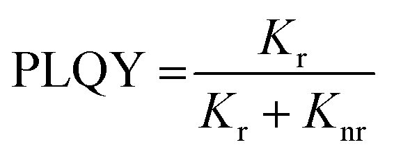
Efficient light-emitting materials are the prerequisite for realizing efficient TPeLEDs. Fig. 1a illustrates the structure and interaction of the quasi-2D blue emitted perovskite with an addition of 2-bromoethylamine hydrobromide (BEABr) used in this work, which has been recently reported by our team.32 The bifunctional molecular BEABr effectively reduces the van der Waals gap and enhances the interaction between the perovskite layers and the emitted wavelength can be shifted to the blue range by controlling the concentration of BEABr. The XRD peaks at 15.5° and 30.8° correspond to the (100) and (200) crystal planes in the perovskite cubic crystal, respectively (Fig. S1, ESI†). And the diffraction peaks located at the (200) crystal planes shift towards lower diffraction angles, indicating that BEABr is introduced into the quasi-2D perovskite lattice as an A+ site spacer cation (Fig. 1a). Fluorescence quantum efficiency (PLQY) and fluorescence lifetime (τavg) are also measured by controlling the BEABr concentration of 10%, 20%, and 30%, respectively. As the BEABr concentration increases, the emitting wavelength of the perovskite films shifted from 494 nm to 480 nm, and further to 469 nm, which is consistent with the blue-shifted absorption edge (Fig. S2, ESI†). The detailed mechanism of the effect of BEABr has been discussed in our previous work.32 The corresponding fluorescence lifetime of quasi-2D blue emitted perovskite films gradually decreases. The PLQYs at 10% and 20% BEABr concentrations are 37% and 38%, respectively, which are not significantly different, while the corresponding τavg values are 6.89 ns and 6.10 ns, respectively. But as the BEABr concentration further increased to 30%, the PLQY and τavg are all reduced. The equation for PLQY and τavg is: | (1) |
 | (2) |
 | ||
| Fig. 1 (a) Schematic diagram of the quasi-2D perovskite crystal structure. (b) PLQY and (c) fluorescence lifetime of the blue quasi-2D perovskite containing 10%, 20% and 30% BEABr. | ||
As mentioned above, the dense and smooth surface morphology is of importance for the top electrode deposition. To observe the morphology of the quasi-2D perovskite films, a 120 nm thick quasi-2D perovskite film (Fig. S3, ESI†) was prepared and tested by scanning electron microscopy (SEM) and atomic force microscopy (AFM), as shown in Fig. 2. Fig. 2a provides an overall view of the surface of the quasi-2D perovskite films with 10% BEABr, displaying good uniformity and flatness despite the potential conductivity decrease resulting from the addition of the organic macromolecules BEABr. While the SEM image appears slightly blurry, the surface uniformity remains discernible. And the surface morphology of 10% BEABr perovskite material films is better than that of perovskite films without BEABr (Fig. S4, ESI†). Fig. 2b illustrates the roughness of the quasi-2D perovskite film as observed through AFM, showcasing a root mean square (RMS) value of 1.288 nm, indicating a smooth surface morphology, which will be conducive to reduced scattering loss and enhanced suitability for subsequent physical vapor deposition of the interfacial layers and the adjustment of DMD electrodes.
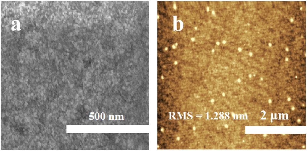 | ||
| Fig. 2 (a) SEM and (b) AFM images of the quasi-2D perovskite films with 10% BEABr. | ||
Fig. 3a presents a schematic representation of the TPeLED device's overall structure, delineating the various material layers employed. All materials are either thermally evaporated or spin-coated onto the transparent indium tin oxide (ITO) substrates. The sequential arrangement of layers from top to bottom includes MoO3/Ag/Cs2CO3/BPhen/TPBi/Perovskite/PEDOT:PSS/ITO/Glass. Each sample utilized in device fabrication comprises four distinct functional zones. Light output measurements are conducted on both of the bottom electrode (ITO side) and top electrode (MoO3 side) of each functional zone, along with assessments of TPeLED light transmittance. In this device structure, TPBi and Bphen not only serve as the electron transport layer and electron injection/hole blocking layer, respectively, but also serve as the dielectric layer of the DMD transparent top electrodes. The Ag layer, as the metal layer in the DMD transparent top electrode, mainly plays a conductive role. The high refractive index MoO3 layer serves as another dielectric layer to adjust the coupling output of light and reduce light loss. In order to ensure electron injection, the thicknesses of TPBi, Bphen, and Cs2CO3 are fixed to the values of the opaque device with a fully reflective metal top electrode. And to balance the electrical and optical properties of TPeLED, 20 nm Ag was deposited on the top electrode, and a high refractive index dielectric layer MoO3 with varying thickness was used to meet the requirements of high EL efficiency and high transmittance. The principle is to exploit the interference between the reflected light waves generated by the front and back surfaces of the film. When the thickness of the film is appropriate, the light reflected on the two faces of the film has a distance difference equal to exactly half a wavelength, and thus cancels each other out. This greatly reduces the reflection loss of light and enhances the intensity of transmitted light. The changes of transmittance of TPeLEDs with different MoO3 thicknesses (ranging from 10 nm to 50 nm) are given in Fig. 3b and c. Notably, both of the maximum transmittance and the transmittance at a wavelength of 494 nm of the TPeLED devices exhibit an initial increase followed by a decrease as the MoO3 thickness increases from 10 nm to 50 nm. And the average transmittance peak values are 68.75% and 65.35%, respectively, which are both achieved at a MoO3 thickness of 30 nm. Moreover, the maximum transmittance shifts from the short wavelength region to the long wavelength region with increasing MoO3 thickness (Fig. S5, ESI†), which further proved the effect of MoO3 thickness on the regulation of TPeLED transmittance.
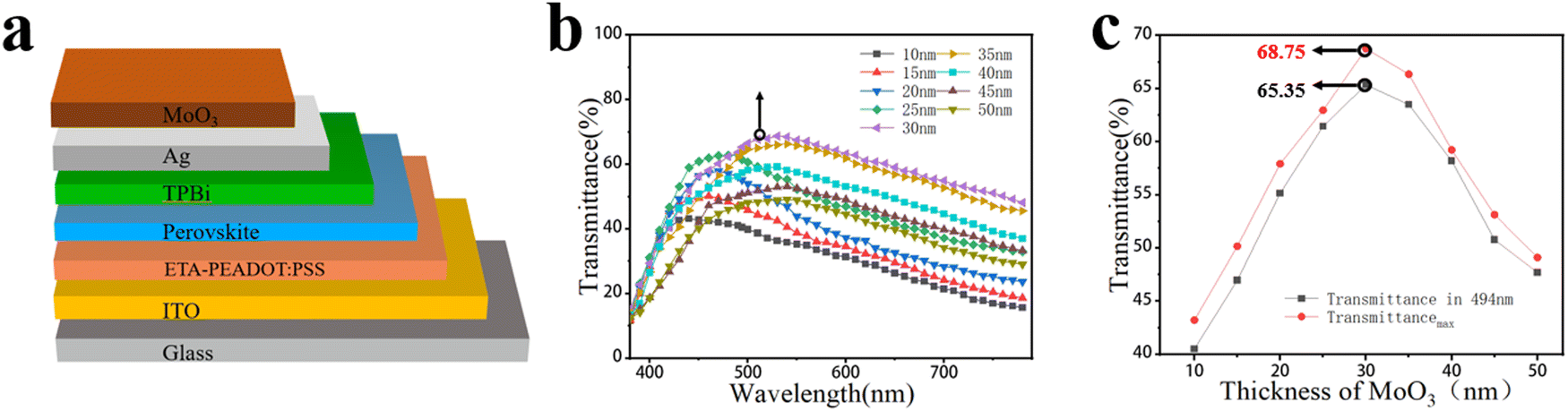 | ||
| Fig. 3 (a) Device structure schematic of the blue TPeLED. (b) Transmittance spectra of the blue TPeLED with different MoO3 thicknesses. (c) Transmittance at the emission wavelength (494 nm) and the maximum transmittance of the blue TPeLED at different MoO3 thicknesses. | ||
In order to further study the influence of MoO3 thickness on the electrical properties of TPeLED devices, we tested the EL properties of TPeLEDs. Since a light-emitting device is transparent, the light emitted by the TPeLEDs will be emitted separately from the two electrodes (ITO side and MoO3 side), so we tested the EL performance from the different electrodes separately (Fig. S6, ESI†). Fig. 4 displays the changes in the maximum brightness and the EQE of the TPeLEDs with varying MoO3 thicknesses, and the detailed spectra are shown in Fig. S7 (ESI†). Both of the changes in Fig. 4 are nearly consistent with the change of the TPeLED transmittance. The peak EQE is obtained at 30 nm MoO3 and the maximum brightness is achieved around 30–35 nm MoO3. This is mainly because the thickness change of MoO3 does not affect the electron injection performance of the cathode, but only affects the optical performance of the device, so its impact on the device EL performance is also reflected by the impact on the brightness. The test resistances of the device are 100.45 Ω cm2 (30 nm MoO3) and 102.25 Ω cm2 (0 nm MoO3), respectively, which can prove that MoO3 does not affect the electron injection efficiency of the device (Fig. S8, ESI†).
 | ||
| Fig. 4 (a) Brightness and (b) EQE of the blue TPeLED measured from the ITO side and MoO3 side, and the total value varies with the thickness of MoO3. | ||
The EL performance, including EQE, current density–voltage (J–V), and brightness, and EL spectrum of the best TPeLEDs are displayed in Fig. 5 and the device parameters are listed in Table 1. The highest EQEs of the best TPeLED with 30 nm MoO3 are 8.54% on the ITO side and 3.19% on the MoO3 side, thus obtaining a total EQE of 11.73% (Fig. 5a). The highest current efficiencies (CEs) of the best TPeLED with 30 nm MoO3 are 8.59% on the ITO side and 2.91% on the MoO3 side, thus achieving a total CE of 11.50% (Fig. 5b). The corresponding brightness is 1650 cd m−2 and 644 cd m−2 measured from the ITO side and MoO3 side, respectively. Simultaneously testing the PLQY on both sides of the device revealed little difference in optical performance between the two sides (Fig. S9, ESI†). The calculated overall brightness of the blue TPeLED is 2294 cd m−2 (Fig. 5c). In order to obtain the light-emitting performance of each side of the electrode, it is necessary to test the light-emitting performance of both sides, so there will be a little inconsistency in the two-sided J–V performance of the device, as seen in Fig. 5b. The blue TPeLED shows a maximum transmittance of 68.75% and a transmittance of 65.35% at an emitted wavelength of 494 nm (Fig. 5c–f).
 | ||
| Fig. 5 (a) EQE, (b) CE, (c) brightness, and (d) transmittance of the device when the MoO3 thickness is 30 nm. (e) Physical image of the working TPeLED. (f) EL spectrum of the blue TPeLED. | ||
| Current efficiency (cd A−1) | Brightness (cd m−2) | EQE (%) | Transmittance (%) | |
|---|---|---|---|---|
| ITO | 8.59 | 1650 | 8.54 | 68.75 |
| MoO3 | 2.91 | 644 | 3.19 | 68.75 |
| Total | 11.50 | 2294 | 11.73 | 68.75 |
Conclusions
In summary, a blue TPeLED has been proposed for the first time. Here a BEABr controlled quasi-2D perovskite is introduced to provide a blue emission and a smooth surface for the preparation of a high-quality top electrode. The top transparent electrode employs a DMD structure electrode, and by adjusting the MoO3 thickness in the top electrode, the TPeLED's transmittance and EL characteristics have been optimized. The best blue TPeLED exhibits a high EQE of 11.73%, an emitted wavelength of 494 nm, together with a high transmittance of nearly 70%, which is competitive performance among the reported TPeLEDs. This work not only provides a feasible device structure for preparing efficient TPeLEDs, but also paves the way for the modulation of TPeLEDs to achieve high transmittance and efficiency of the same device.Experimental
Materials
Cesium bromide (CsBr) and lead bromide (PbBr2) were purchased from Xi'an Yuri Solar Co, Ltd. Phenylethylammonium bromide (PEABr) was purchased from Sigma Aldrich. Benzyltrimethylammonium bromide (BEABr) was purchased from Aladdin. All materials were used directly without further purification.Preparation and characterization of perovskite films
The powders of CsBr, PbBr2, and PEABr (in a molar ratio of 6![[thin space (1/6-em)]](https://www.rsc.org/images/entities/char_2009.gif) :5:4) were added to anhydrous DMSO solvent and stirred at 40 °C for 2 hours. A transparent perovskite precursor solution with a concentration of 0.175 mM was obtained. Afterwards, 0.015 mmol, 0.03 mmol, and 0.045 mmol of BEABr were added to 2 ml of transparent perovskite precursor solution, respectively, to form 10%, 20%, and 30% BEABr blue-emitted quasi two-dimensional perovskite solutions with different concentrations. Then the obtained solution was spin coated on glass at 4500 rpm for 60 seconds. After spin coating, the substrate was baked on a hot plate at 70 °C for 10 minutes. The morphology of films was characterized using a Hitachi 4800 scanning electron microscope. The surface roughness was analyzed with a Shimadzu SPA-9700 atomic force microscope. The absorption spectra of the films were measured with a Shimadzu UV-3101PC spectrophotometer. The PL spectra of the films were measured by using a Hitachi F-7000 fluorescence spectrometer. Time-resolved EL spectra of the films were measured with an Edinburgh FLS920 fluorescence spectrometer, on which fluorescence quantum yield measurements were performed with a calibrated integrating sphere. The XRD patterns of perovskite films were measured by using a Rigaku SmartLab X-ray diffractometer. The reflectance spectra were measured using a UV-visible-near infrared spectrophotometer (Lambda 1050, PerkinElmer). All measurements were performed at room temperature under ambient conditions.
:5:4) were added to anhydrous DMSO solvent and stirred at 40 °C for 2 hours. A transparent perovskite precursor solution with a concentration of 0.175 mM was obtained. Afterwards, 0.015 mmol, 0.03 mmol, and 0.045 mmol of BEABr were added to 2 ml of transparent perovskite precursor solution, respectively, to form 10%, 20%, and 30% BEABr blue-emitted quasi two-dimensional perovskite solutions with different concentrations. Then the obtained solution was spin coated on glass at 4500 rpm for 60 seconds. After spin coating, the substrate was baked on a hot plate at 70 °C for 10 minutes. The morphology of films was characterized using a Hitachi 4800 scanning electron microscope. The surface roughness was analyzed with a Shimadzu SPA-9700 atomic force microscope. The absorption spectra of the films were measured with a Shimadzu UV-3101PC spectrophotometer. The PL spectra of the films were measured by using a Hitachi F-7000 fluorescence spectrometer. Time-resolved EL spectra of the films were measured with an Edinburgh FLS920 fluorescence spectrometer, on which fluorescence quantum yield measurements were performed with a calibrated integrating sphere. The XRD patterns of perovskite films were measured by using a Rigaku SmartLab X-ray diffractometer. The reflectance spectra were measured using a UV-visible-near infrared spectrophotometer (Lambda 1050, PerkinElmer). All measurements were performed at room temperature under ambient conditions.
Device fabrication and characterization
The device structure of TPeLEDs, from top to bottom, consists of a MoO3/Ag/Cs2CO3/BPhen/TPBi/Perovskite/PEDOT:PSS/ITO/Glass stack. PEDOT:PSS layer and perovskite luminescent layer are prepared by spin coating. PEDOT:PSS was spin coated on glass with ITO at 2500 rpm for 40 seconds. After spin coating, the substrate was baked on a hot plate at 140 °C for 15 minutes. Afterwards, perovskite thin films were prepared. TPBi, BPhen, Cs2CO3, Ag, and MoO3 layers were deposited by thermal evaporation in a vacuum of 3 × 10⁻⁵ Pa, with deposition rates of 1 Å s−1, 1 Å s−1, 1 Å s−1, 7–10 Å s−1, and 3–5 Å s−1, respectively. Scanning electron microscopy (SEM) imaging was conducted using the Hitachi S4800 instrument, while atomic force microscopy (AFM) analysis was performed using the Shimadzu SPA-9700 system. Electroluminescence (EL) spectra were measured using the Shimadzu F-7000 spectrometer. The transmission spectrum was collected using the Shimadzu UV3101PC spectrophotometer. For electrical characterization, a Keithley 2611 source measurement unit in conjunction with a Konica Minolta LS-110 brightness meter was employed to obtain the current density–voltage (J–V) and brightness–voltage (L–V) characteristics.Conflicts of interest
There are no conflicts to declare.Acknowledgements
This work was supported by the National Natural Science Foundation of China (No. 62175235 and 62035013), the Jilin Province Science and Technology Research Project (20220201091GX, 20230101366JC, and 20220201064GX), the Changchun Science and Technology Development Plan Project 23SH06, and the Project supported by the Dawn Talent Training Program of CIOMP.Notes and references
- S. Hou, J. Liu, F. Shi, G. X. Zhao, J. W. Tan and G. Wang, Front. Chem., 2022, 10, 864186 CrossRef CAS PubMed.
- B. Zhang, R. Gong, Y. Zhang, Y. Li and L. Zhu, Nanotech. Rev., 2023, 12(1), 20230578 CrossRef CAS.
- Y. F. Liu, J. Feng, Y. G. Bi, D. Yin and H. B. Sun, Adv. Mater. Technol., 2019, 4(1), 1800371 CrossRef.
- V. C. Nair, C. Muthu, A. L. Rogach, R. Kohara and V. Biju, Angew. Chem. Int. Ed., 2017, 56(5), 1214–1218 CrossRef CAS PubMed.
- J. Fan, Q. Lv, Q. Yang, X. Song, Y. Han, B. Wang and P. Guo, Chemistry, 2023, 86(6), 665–681 CAS.
- Y. Cao, N. Wang, C. Yi, L. Zhu and J. Wang, Acta Optica Sinica, 2022, 42(17), 1733001 CrossRef.
- H. Cheng, Y. Feng, Y. Fu, Y. Zheng, Y. Shao and Y. Bai, J. Mater. Chem. C, 2022, 10(37), 13590–13610 RSC.
- C.-H. Gao, Y. Zhang, X.-J. Ma, F.-X. Yu, Y.-L. Jia, Y.-L. Lei, P. Chen, W.-W. Sun and Z.-H. Xiong, Org. Electron., 2018, 58, 88–93 CrossRef CAS.
- Z. Zhu, Y. Wu, Y. Shen, J. Tan, D. Shen, M.-F. Lo, M. Li, Y. Yuan, J.-X. Tang, W. Zhang, S.-W. Tsang, Z. Guan and C.-S. Lee, Chem. Mater., 2021, 33(11), 4154–4162 CrossRef CAS.
- Z. Feng, L. Wang, H. Yu, X. Ma, Q. Zhang, S. Chen, L. Liu and W. Huang, Org. Electron., 2018, 61, 18–24 CrossRef CAS.
- L. Cai, J. G. Zhou, G. L. Bai, J. Q. Zang, A. El-Shaer, T. Song, M. K. Fung and B. Q. Sun, Adv. Opt. Mater., 2022, 10, 202101137 Search PubMed.
- L. Liu, K. Cao, S. Chen and W. Huang, Adv. Opt. Mater., 2020, 8(22), 2001122 CrossRef CAS.
- H. P. Kim, J. Kim, B. S. Kim, H.-M. Kim, J. Kim, A. R. B. M. Yusoff, J. Jang and M. K. Nazeeruddin, Adv. Opt. Mater., 2017, 5(7), 1600920 CrossRef.
- Y. Ye, W. Zhang, Y. Zhang, K. Li, J. Han and C. Liu, Chem. Eng. J., 2022, 445, 136867 CrossRef CAS.
- S. Yuan, L. J. Dai, Y. Q. Sun, F. Auras, Y. H. Zhou, R. Z. An, Y. Liu, C. F. Ding, C. Cassidy, X. Tang, S. C. Dong, H. B. Kang, K. Chen, X. M. Liu, Z. F. Ye, Y. X. Zhao, C. Adachi, L. S. Liao, N. C. Greenham and R. H. Friend, Nat. Photonics, 2024, 1749–4885 Search PubMed.
- H. W. Lee, H. S. Lee, J. W. Lee, J.-H. Kim, K.-H. Lee, S. M. Cho, H. Yang, J. Park and Y. K. Kim, Polym. Bull., 2016, 73(9), 2583–2591 CrossRef CAS.
- Y. Shen, M.-N. Li, Y. Li, F.-M. Xie, H.-Y. Wu, G.-H. Zhang, L. Chen, S.-T. Lee and J.-X. Tang, ACS Nano, 2020, 14(5), 6107–6116 CrossRef CAS PubMed.
- J. Lv, L. Fang and J. Shen, Mater. Lett., 2018, 211, 199–202 CrossRef CAS.
- H. K. Seo, H. Kim, J. Lee, M. H. Park, S. H. Jeong, Y. H. Kim, S. J. Kwon, T. H. Han, S. Yoo and T. W. Lee, Adv. Mater., 2017, 29(12), 1605587 CrossRef PubMed.
- G. Li, F. W. R. Rivarola, N. J. L. K. Davis, S. Bai, T. C. Jellicoe, F. Pena, S. Hou, C. Ducati, F. Gao, R. H. Friend, N. C. Greenham and Z.-K. Tan, Adv. Mater., 2016, 28(18), 3528 CrossRef CAS PubMed.
- K. Sun, Z. Q. Bao, X. Y. Guo, D. Y. Zou, Y. Lv, J. C. Liang and X. Y. Liu, Adv. Opt. Mater., 2024, 12(5), 202301752 Search PubMed.
- J. Q. Liang, X. Y. Guo, L. Song, J. Lin, Y. S. Hu, N. Zhang and X. Y. Liu, Appl. Phys. Lett., 2017, 111(21), 213301 CrossRef.
- H. Wu, Y. Zhang, X. Y. Zhang, M. Lu, C. Sun, X. Bai, T. Q. Zhang, G. Sun and W. W. Yu, Adv. Electron. Mater., 2018, 4(1), 1700285 CrossRef PubMed.
- C. C. Xie, X. F. Zhao, E. W. Y. Ong and Z. K. Tan, Nat. Commun., 2020, 11(1), 4213 CrossRef CAS PubMed.
- Z. Wang, F. Wang, W. Sun, R. Ni, S. Hu, J. Liu, B. Zhang, A. Alsaed, T. Hayat and Z. A. Tan, Adv. Funct. Mater., 2018, 28(47), 1804187 CrossRef.
- Z. B. Wang, F. Z. Wang, B. Zhao, S. N.Qu, T. Hayat, A. Alsaedi, L. Z. Sui, K. J. Yuan, J. Q. Zhang, Z. X. Wei and Z. A.Tan, J. Phys. Chem. Lett., 2020, 11(3), 1120 CrossRef CAS.
- L. M. Kong, X. Y. Zhang, Y. G. Li, H. R. Wang, Y. Z. Jiang, S. Wang, M. Q. You, C. X. Zhang, T. Zhang, S. V. Kershaw, W. T. Zheng, Y. G. Yang, Q. Q. Lin, M. J. Yuan, A. L. Rogach and X. Y. Yang, Nat. Commun., 2021, 12(1), 1246 CrossRef CAS PubMed.
- Z. Li, Z. Chen, Y. Yang, Q. Xue, H.-L. Yip and Y. Cao, Nat. Commun., 2019, 10, 1027 CrossRef PubMed.
- F. Z. Wang, Z. Y. Wang, W. D. Sun, Z. B. Wang, Y. M. Bai, T. Hayat, A. Alsaedi and Z. A. Tan, Small, 2020, 16(32), 2002940 CrossRef CAS PubMed.
- Y. Yang, X. Yang, L. He, J. Gao, Y. Lian and X. Yang, Acta Opt. Sin., 2021, 41(17), 1716001 CrossRef.
- Z. Chu, W. Zhang, J. Jiang, Z. Qu, F. Ma, Y. Zhao, X. Chu, Y. Shen, Y. Li, Z. Yin, X. Zhang and J. You, Nat. Electron., 2023, 6(5), 360–369 CrossRef CAS.
- Z. Q. Bao, L. Yu, S. X. Y. Guo, Y. P. Wang, Y. Lv, D. Y. Zou, L. Song and X. Y. Liu, Chem. Eng. J., 2024, 482, 148875 CrossRef CAS.
Footnote |
| † Electronic supplementary information (ESI) available. See DOI: https://doi.org/10.1039/d4tc00934g |
| This journal is © The Royal Society of Chemistry 2024 |