
 Open Access Article
 This Open Access Article is licensed under a Creative Commons Attribution-Non Commercial 3.0 Unported Licence
Transition of photoresponsivity in graphene–insulator–silicon photodetectors†
Hong-Ki
Park
and
Jaewu
Choi
 *
*
Quantum Information Display Laboratory, Department of Information Display, Kyung Hee University, 26, Kyungheedae-ro, Dongdaemun-gu, Seoul, 02447, Republic of Korea. E-mail: jaewuchoi@khu.ac.kr
First published on 7th May 2024
Abstract
The photocurrent and photoresponsivity of majority-carrier type graphene–insulator–silicon (MC-GIS) photodetectors exhibit a transition from positive to negative as the illuminating optical power decreases below a critical threshold. This transition coincides with a photoinduced alteration of the Schottky barrier height (SBH) relative to its dark state. Interestingly, when the optical power falls below this critical optical power, a notably high negative photoresponsivity (NPR) emerges. This NPR phenomenon is attributed to the photoinduced elevation of the SBH rather than its reduction. For instance, at an optical power of 8.32 nW and a reverse bias voltage of 5 V, the NPRs for red and green LED light illuminations reach approximately −18![[thin space (1/6-em)]](https://www.rsc.org/images/entities/char_2009.gif) 600 A W−1 and −14000 A W−1, respectively. The unusual sign change of photocurrent and photoresponsivity depends on the competition between photoinduced band bending and photoinduced voltage redistribution among graphene, insulator and silicon. This switching mechanism is universally applicable to graphene–insulator–silicon photodetectors and beyond.
600 A W−1 and −14000 A W−1, respectively. The unusual sign change of photocurrent and photoresponsivity depends on the competition between photoinduced band bending and photoinduced voltage redistribution among graphene, insulator and silicon. This switching mechanism is universally applicable to graphene–insulator–silicon photodetectors and beyond.
1. Introduction
The demand for highly sensitive photodetectors is steadly increasing in various modern applications, including smartphones, telecommunications, suvallience, security, unmaned mobile systems, augmented reality, merged reality, quantum optics, quantum science and quantum technologies, etc.1–12 In pursuit of this objective, extensive research has been conducted on silicon and graphene, leveraging their unique properties.13–19 Graphene, with its symmetrical linear energy dispersion at low energies, high carrier mobility, strong carbon sp2 hybridization-based bonding structure, mechanical flexibility, atomically thin profile, and high optical transmittance across the visible spectrum, is an ideal functional material and structure for optoelectronic devices spanning a broad spectral range.13–16 In particular, over the past decade, significant attention has been devoted to graphene–silicon (GS) or graphene–insulator–silicon (GIS) photodiodes.17–21In contrast to minority-carrier type photodiodes, majority-carrier type graphene–insulator–silicon (MC-GIS) photodiodes exhibit remarkable characteristics, including exceptionally high responsivity, fast on–off response time, and high detectivity22–25 These notable features are attributed to the photoinduced energy redistribution across the junctions. This redistribution leads to a lowering of the Schottky barrier height (SBH) through the shift of the graphene Fermi level and an increase in the acting voltage on the insulator layer.22–25 Furthermore, the incorporation of an overlayer on graphene, such as poly methyl methacrylate (PMMA, (C5O2H8)n), serves a dual purpose. Firstly, it acts as a protective layer, exhibiting high transmittance within the visible spectral range.23 Secondly, it effectively modulates the physical gap between graphene and silicon, thereby playing a crucial role in the modulation of the Schottky barrier height (SBH).23 Utilizing these properties, highly efficient majority-carrier type graphene–insulator–silicon (MC-GIS) photodiodes have been successfully demonstrated for red (R) and blue (B) light.22–24 Moreover, the MC-GIS structure using silicon on insulator (SOI) has enabled the development of highly efficient color photodetectors for red, green, and blue (B) light, which can operate at low bias voltages.25 These exceptional characteristics hold great promise for the advancement of graphene-based optoelectronic devices in the next generation.22–25
Furthermore, the ability to detect extremely low level signals is crucial for various applications such as unmanned vehicles, surveillance, and monitoring systems. Traditionally, avalanche photodiodes (APD) operating at high bias voltages are employed to fulfill these requirements.7–10 However, the unique properties of MC-GIS photodiodes offer an alternative approach for achieving high sensitivity without the need for high bias voltages, opening up new possibilities for such applications.22–25
In this investigation, we introduce another characteristic of a majority carrier-type graphene–insulator–silicon (MC-GIS) photodetector, demonstrating a distinctive transition between positive photocurrent (PPC) and negative photocurrent (NPC) with exceptionally high responsivity, contingent upon the incident light intensity. This switching behavior in photocurrent and photoresponsivity is ascribed to the modulation of the photoinduced Schottky barrier height (SBH) relative to its dark state value.22–27 The optical power-dependent switching mechanism elucidated in this study holds universal relevance across graphene–insulator–silicon photodetectors and extends beyond.
2. Results and discussion
2.1. Current–voltage characteristics of MC-GIS
MC-GIS photodetectors are composed of three key components: graphene, a very thin insulator layer, and lightly doped p-type silicon as shown in the inset of Fig. 1a. The comprehensive fabrication process for MC-GIS photodetectors, along with the characterization setup (the inset of Fig. 1b) utilized for investigating their performance, are depicted schematically in the ESI† (Section S1). Additionally, in the ‘Experimental section’, one can find a thorough description of the experimental methods employed in this study. | ||
| Fig. 1 Current (I) – voltage (V) characteristic curves for (a) red (640 nm), and (b) green (532 nm) light illuminations. The inset in (a) shows the optical image of the graphene–insulator–silicon (GIS) structure while the inset in (b) shows schematically the experimental setup for photo-response study of GIS. | ||
Fig. 1 illustrates the current–voltage (I–V) characteristics of the MC-GIS photodetectors under different conditions. Specifically, the curves display the dark current (ID) and the current under red (640 nm) (Fig. 1a) and green (532 nm) (Fig. 1b) LED light illuminations (IP). It is observed that the current primarily exhibits variations in the reverse bias region in response to the optical power as expected. Notably, the current under light illumination (IP) can be either higher or lower than the dark current (ID) in the reverse bias voltage regions, depending on the optical power, as illustrated in Fig. 1.
2.2. Dark current–voltage characteristics of MC-GIS
In this study, the dark current behaviors (ID) of the MC-GIS structures are investigated and described using a modified Schottky emission theory that incorporates a tunneling term, expressed as .22–25,28 Here ξ a represents the tunneling barrier height, and d refers to the thickness of the thin insulator layer.
| ID = IDS〈exp{[q(V − IDRs)]/(ηekBT)} − 1〉 | (1) |
 | (2) |
| ΦDs(V) = ϕD0 + ΔVDox(V) + ΔVDG(V) | (3) |
In the presented equations, ΦDs(V) represents the voltage-dependent effective Schottky barrier height (SBH) in volt while ηe(V) denotes the voltage-dependent effective ideality factor. Several parameters are involved, including A (junction area), A* (effective Richardson constant), T (absolute temperature), q (elemental charge), kB (Boltzmann constant), and Rs (series resistance). The voltage-dependent SBH (eqn (3)) is the sum of three terms: ϕD0, ΔVDox(V), and ΔVDG(V). These terms represent the SBH at zero bias voltage, the variation of the oxide voltage at V, and the shift of the graphene Fermi level in volt at V, respectively. These equations have been adapted from previous reports for understanding the voltage dependence of the SBH in the MC-GIS structures.22–25 From this, the investigated GIS photodiodes in this study show the estimated Schottky barrier height (SBH) of approximately ∼0.3 eV, which is lower than the half of the energy band gap of the semiconductor material. Further ξ and d are estimated as 3.3 eV and 5.75 Å, respectively. This clearly indicates that the GIS photodiodes are majority carrier type.22–27
2.3. Positive and negative photocurrents
From Fig. 1, it is evident that the reverse bias voltage-dependent net photocurrent (Iph = IP − ID) of the MC-GIS photodetector exhibits both positive and negative values, depending on the optical power. Fig. 2 provides a visual representation of this behavior for red (640 nm) (Fig. 2a) and green (532 nm) (Fig. 2b) light illuminations. Notably, when the optical power surpasses 2.29 μW, the photocurrent (Iph) is predominantly positive, aligning with previous research findings.22–25 However, when the optical power falls below 2.29 μW, the photocurrent becomes negative for both red and green LED light illuminations. At an optical power of 2.29 μW, the photocurrent shows a transition point. Specifically, at lower reverse bias voltages, the photocurrent is negative, while at higher reverse bias voltages exceeding the crossing voltage (Vx), the photocurrent becomes positive. The crossing voltage (Vx) represents the point at which the photocurrent becomes zero (Iph(Vx) = 0). | ||
| Fig. 2 Switching behavior of the photocurrent as a function of optical power for two different light illuminations: (a) red (640 nm) and (b) green (532 nm). The plot showcases the transition between positive and negative photocurrents at varying optical power levels for each specific light wavelength. | ||
For optical power illuminations higher than 2.29 μW, the voltage-dependent positive photocurrent (PPC) behavior can be categorized into three regions, as previously reported.20–22 Let's discuss these regions using the example of red light illumination with an optical power of 105 μW shown in Fig. 2a. In the first region, which is the low reverse bias voltage region (VR: 0–0.6 V), the depletion region is small or negligible.22 The initial band bending is small due to the small work function difference between graphene and p-type silicon or the built-in voltage. At low bias voltages, the slow drift and diffusion velocity cause the high recombination of photogenerated carriers and result in the low photocurrent.
The second region is the intermediate reverse bias voltage region (VR: 0.6–3.3 V). In this region, the depletion region expands proportionally with the reverse bias voltage. As a result, the portion of incident photons absorbed in the depletion region increases with the reverse bias voltage. Photogenerated holes quickly transit to the electrode as the reverse bias voltage increases, leading to a reduction in recombination probability. Simultaneously, some of photogenerated electrons (minority carriers) accumulate at the interface between the silicon and silicon oxide and the other of them tunnel to the graphene electrode. At the same time, the conductance of the light absorbing silicon increases with optical power. As a result, the given applied voltage is redistributed differently from that at the dark state. This increases the oxide voltage acting on the oxide layer and shifts the graphene Fermi level. This lowers the Schottky barrier height (SBH), and increases the photocurrent with the reverse bias voltage, as previously reported.22–25
In the third region (VR higher than 3.3 V), the photocurrent with reverse bias voltage reaches saturation. However, the onset voltage for the peak or saturation within the reverse bias range (VR: 2.6–3.3 V) decreases with higher optical power. Interestingly, this behavior is less sensitive to the wavelength of the illumination, despite the distinct absorption coefficients observed for different wavelengths.
After reaching the onset voltages for peak or saturation, the photocurrent starts to decrease slightly with increasing reverse bias voltage and eventually either slowly decreases or saturates. This behavior is more pronounced in the case of green light illuminations, as shown in Fig. 2b.17 The slight lowering of the photocurrent after the onset voltage is primarily attributed to the increasing tunneling rate. As the reverse voltage increases further, the photocurrent either saturates or slowly increases. The slower process observed at higher reverse voltages is related to the increasing voltage acting on the photogenerated carriers in the resistive diffusion region (see S2 (photo-capacitance), ESI†).22,29
The observed enhancement in positive photocurrent is in line with the expected behavior of MC-GIS photodetectors, as reported in previous studies.22–25 This enhancement is attributed to the photoinduced lowering of the Schottky barrier height (SBH), which is achieved through photoinduced voltage redistribution, enhanced voltage acting on the insulator, and Fermi level shift in graphene. Consequently, the photocurrent generally increases with both the optical power and the applied bias voltage, as shown in Fig. 2.
In contrast to the positive photocurrent behaviors at the relatively high optical power illumination, the negative photocurrent (NPC) for the relatively low light illumination exhibits an almost linear increase with reverse bias voltage. The NPC for green light illumination initially shows a linear increase and then increases with a lower slope. These NPC behaviors will be further elucidated in the subsequent sections, particularly in the analysis of photoresponsivity.
2.4. Positive photoresponsivity and V-dependent switching to negative photoresponsivity
The photoresponsivity is the ratio of the photocurrent to the optical power. In Fig. 3a and b, the photoresponsivity is presented for red (640 nm) and green (532 nm) LED lights, respectively, at relatively high optical powers ranging from 2.29 μW to 105 μW. In Fig. 3a, the positive photoresponsivity (PPR) is higher at logner wavelength, as expected. However, it decreases with higher optical power, following the usual trend. The peak responsivities are observed at lower bias voltages as the optical power decreases. For red light illumination, the peak responsivity of approximately 10.5 A W−1 is observed at a reverse bias voltage of around 3 V, with an optical power of 16.8 μW. Similarly, in Fig. 3b, for green light illumination, the positive responsivity also decreases with higher optical power. The peak responsivity of approximately 7 A W−1 is observed at a reverse bias voltage of around 3 V, with an optical power of 16.8 μW.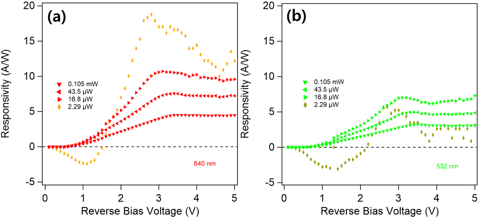 | ||
| Fig. 3 Photoresponsivity as a function of reverse bias voltage for red (a) and green (b) light illuminations with optical powers higher than 2.29 μW. | ||
At an optical illumination of 2.29 μW, the responsivity exhibits voltage-dependent switching behaviors. The photoresponsivity is negative at lower bias voltages than the crossing voltage (Vx) but becomes positive as the bias voltage increases beyond Vx. The photocurrent is zero at the crossing voltage (Vx). For the red light illumination, the crossing voltage (Vx) is observed at around 1.5 V, while for the green light illumination, it is observed at around 2 V. The positive peak responsivities are approximately 18 A W−1 and 5 A W−1 for the red and green light, respectively. On the other hand, the negative peak responsivities are approximately −2.5 A W−1 and −3 A W−1 for the red and green light, respectively.
2.4. Optical power dependent switching to high negative photoresponsivity
Fig. 4a and b display the photoresponsivity at relatively low optical power illuminations (ranging from 8.32 nW to 2.29 μW) for red (640 nm) and green (532 nm) light emitting diode (LED) lights, respectively. In this regime, the photocurrent remains negative within the employed reverse bias voltage ranges. As the optical power decreases below 2.29 μW, the magnitudes of the negative photoresponsivity (NPR) for red and green light illuminations become negatively larger. For instance, at an optical power of 8.32 nW, NPRs are −18600 A W−1 for red light and −14000 A W−1 for green light, both measured at a reverse bias voltage of 5 V. These NPR are three orders of magnitude higher than the highest positive photoresponsivity (PPR) observed in Fig. 3 and 4.
 | ||
| Fig. 4 Negative photoresponsivity (NPR) as a function of optical power illuminations. (a) and (b) photoresponsivity as a function of reverse bias voltage for optical power illuminations less than 2.29 μW for red (640 nm) and green (532 nm) light, respectively. | ||
NPR for red light increases linearly with the reverse bias voltage, whereas the NPR for green light exhibits a higher rate of increase at low bias voltages compared to the NPR for red light. However, at higher reverse bias voltages, the rate of increase for the NPR of green light becomes slower than that of red light. Consequently, before the deflection point in the plot, the NPR for green light surpasses that of red light. However, after the deflection point, the NPR for red light becomes higher than that of green light, as illustrated in Fig. 4. This is attributed to the wavelength dependent light absorption depth while the depletion depth just depends on the reverse bias voltage.
2.5. Light induced Schottky barrier height modulations
Based on the modified Schottky emission theory at both dark (ID) and under light illumination (Ip), the net photocurrent (Iph) can be approximated as follows (for more detailed information, please refer to the ESI† in Section S3):| Iph = IDS(exp(−qΔΦPs)/(kBT))〈exp{[q(V − IPRs)]/(ηekBT)} − 1〉 − IDS 〈exp{[q(V − IDRs)]/(ηekBT)} − 1〉 | (4) |
In this equation, qΔΦPs denotes the photoinduced Schottky barrier height (SBH) variation compared to the SBH at the dark state (qΦDs). When ΔΦPs is equal to zero, the net photocurrent (Iph) becomes zero as expected and the correponding voltage is the crossing voltage (Vx). The photocurrent (Iph) is dierectly proportional to the dark current (ID) and is an exponential function of the SBH modulation (qΔΦPs) as shown in eqn (4).
The modified Schottky emission theory shown in eqn (4) allows to extract the modulation of the Schottky barrier hieght (qΔΦPs) from the experimental current–voltage curves as shown in eqn (5). (for details, see ESI,† S3)
 | (5) |
The second term in eqn (5) is relatively minor compared to the first term. Thus, the modulation of the Schottky barrier hieght (qΔΦes) can be approximated as
 | (6) |
This clearly shows that the modulation of the Schottky barrier hieght (qΔΦPs) can be experimentally determined without any exsorting to the fitting parameters of the current–voltage curves. This clearly indicates that the SBH increases logarithmaticcaly with the ratio of the dark current to the current under the illumination.
The extracted modulation of the Schottky barrier height (qΔΦPs) as a function of the reverse bias voltage is presented in Fig. 5a and b for red (640 nm) and green (532 nm) light illuminations at various optical powers. This clearly shows that the sign of the SBH modulation (ΔΦPs) (Fig. 5) determins the sign of the photocurrent as observed in Fig. 1–4. At optical powers below the critical value, the modulation of the SBH (ΔΦPs) becomes positive, as depicted in Fig. 5a and b. The observed SBH modulation in Fig. 5a and b provides clear insights into the amplification (magnitude of SBH modulation) and switching (sign of SBH modulation) mechanisms underlying the photocurrent and photoresponsivity behaviors depicted in Fig. 1–4 (see ESI,† S3).
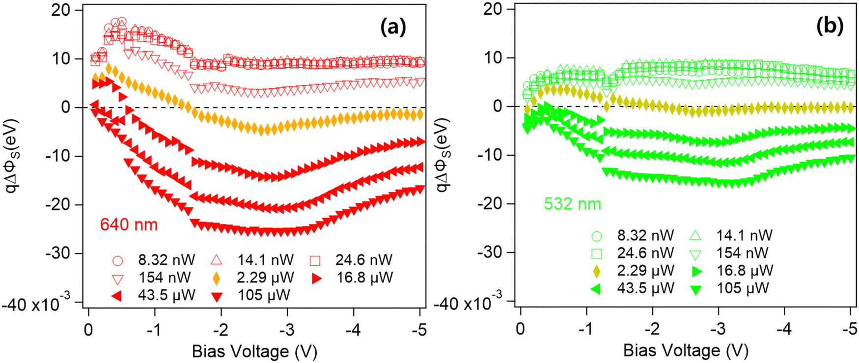 | ||
| Fig. 5 Optical power dependent Schottky barrier height modulation as a function of reverse bias voltage for (a) red (640 nm) and (b) green (532 nm) light illuminations. | ||
Additionally, the voltage (V) dependent switching (at 2.29 μW) of the photocurrent, photoresponsivity and SBH modulation consistently occurs across the crossing voltages (Vx) as shown in Fig. 2–5. At the lower bias voltage than the crossing voltage (Vx), the amount of the accumulated steady-state minority carrier (or negative charge) in semiconductor is higher than that at dark while the photoinduced conductivity change is minor. As a result, the SBH is higher than that at dark state. Then the photocurrent and the photoresponsivity becomes negative (Fig. 2 and 3) while SBH modulation is positive (Fig. 5).
As the bias voltage increases beyond the crossing voltage, several effects come into play. Firstly, the expansion of the depletion region leads to an increase in the steady-state excess charge in the semiconductor. Consequently, both the oxide voltage and the graphene Fermi level shift become higher than their values in the dark condition. Additionally, the conductance in the depletion region becomes higher compared to that at dark state. As depicted in Fig. 5a and b, this leads to a lowering of the SBH, thereby enabling the generation of positive photocurrent and positive photoresponsivity, as observed in Fig. 2 and 3.
Furthermore, it is worth noting that the crossing voltage Vx (Iph = 0) depends on the wavelength. This can be attributed to the fact that the photocarrier generation rate varies with wavelength for a given optical power. Specifically, for the same optical power, the photocarrier generation rate is 1.203 times higher for red light (640 nm) compared to green light (532 nm). Consequently, the transition from negative photoresponsivity (NPC) to positive photoresponsivity (PPC) occurs at a higher bias voltage for green light compared to red light. Even at the higher optical power of 16.8 μW than 2.29 μW, when considering the low bias voltage range, the photocurrent remains negative for red light illumination, as clearly depicted in the SBH variation shown in Fig. 5.
2.6. Switching of photocurrent, photoresponsivity and SBH modulation
Fig. 6 illustrates the absolute values of the photocurrent (Fig. 6a) and the photoresponsivity (Fig. 6b), along with the light-induced SBH modulation (Fig. 6c) and the absolute value of SBH modulation per optical power (Fig. 6d), all plotted against the optical power at a reverse bias voltage of 5 V for red (640 nm) and green (532 nm) light illuminations. Three distinct regions are observed: the negative region, transition region, and positive region of the photocurrent. | ||
| Fig. 6 Photocurrent and photoresponsivity are plotted as functions of optical power for red (640 nm) and green (532 nm) light illuminations. Absolute values of (a) photocurrent and (b) photoresponsivity are shown as functions of optical power for red and green light at a reverse bias voltage of 5 V, respectively. (c) Depicts light-induced SBH modulation at 5 V for red and green light illuminations. (d) Shows the absolute value of light-induced SBH modulation at 5 V per optical power for red and green light illuminations. | ||
In the positive region, the photocurrent (Fig. 6a) behaves as expected, increasing with optical power. However, in the negative region, the photocurrent demonstrates an inverse relationship with optical power, becoming less sensitive to changes in optical power as it decreases below a certain threshold. Notably, for green light illuminations, the photocurrent decreases as the optical power decreases after reaching the optical power corresponding to the negative peak photocurrent. This suggests the presence of a limiting factor for the negative photocurrent in this region.
The switching behavior of photoresponsivity is evident in Fig. 6b. Negative photoresponsivity (NPR) is clearly three orders higher than positive photoresponsivity (PPR).
Fig. 6c specifically illustrates the photoinduced SBH modulation at a reverse bias voltage of 5 V as a function of optical power. As expected, the SBH modulation is positive at lower optical powers, while it becomes negative for optical powers exceeding the critical power threshold. In the negative photocurrent region, as the optical power decreases, the SBH modulation initially increases until it reaches a peak point, after which it starts to slowly decrease.
In the positive photocurrent region, the SBH modulation negatively increases with optical powers. However, the photoresponsivity decreases as the optical power increases, as depicted in Fig. 6b. This is attributed to the higher resistive loss (IR) due to the increased photocurrent (refer to eqn (4)). This observed trend in the SBH modulation aligns with the corresponding variations in the photocurrent and photoresponsivity.
Fig. 6d provides a clear illustration of the absolute value of the photoinduced SBH modulation per optical power. This plot highlights the efficiency of the negative photoresponsivity (NPR) compared to the positive photoresponsivity (PPR). The efficiency of SBH modulation is exceptionally high in the region of negative photocurrent. The variation of the absolute value of SBH modulation with optical power (Fig. 6d) exhibits a similar trend to that of responsivity (Fig. 6b).
Based on the aforementioned observations, particularly the experimentally extracted SBH modulation, we propose mechanisms for negative photocurrent (NPC), positive photocurrent (PPC), and the switching behaviors of photocurrent as outlined below.
3. Switching between negative photocurrent and positive photocurrent
The origin of negative photocurrent in photodetectors has been a subject of debate. Several factors, primarily related to the reduction of free charge carrier density and carrier mobility, have been proposed to elucidate negative photoconductivity.30–36 These factors include hot carrier trapping,30,34 mobility reduction due to scattering caused by adsorbates and photo-induced phonons,30,31,33 and the presence of coupled defect levels in the energy band gap.30,35,36 However, their applicability in explaining negative photoconductivity is often limited to specific systems and scenarios. Notably, adsorbates on the surface and trap charged states at the interface play a significant role in explaining negative photoconductivity in low-dimensional materials systems, such as graphene,30–32,34 while coupled defect levels in the gap play significant roles in explaining negative photoconductivity in three-dimensional materials systems as well as nanostructures.30,35,36In this study, we present a distinct and plausible mechanism to explain the observed phenomenon of negative photocurrent and switching behaviors. Fig. 7a illustrates the energy band diagrams of reversely biased MC-GIS photodetectors consisting of CVD-grown graphene, native silicon oxide insulator, and lightly doped p-type silicon in the dark state. The p-type silicon (100) substrate has a low doping level with a resistivity ranging from 1 to 10 Ω cm. The Fermi level (EFS) of the silicon lies between the intrinsic Fermi level (Ei) and the valence band maximum (EV). The difference in work function (EFG − EFS) between p-type silicon (EFS) and graphene (EFG) is relatively small, resulting in minimal band bending in both the silicon (φs) and insulator regions under equilibrium conditions.
 | ||
| Fig. 7 Schematic energy band diagrams of the graphene (G), insulator (I), and p-type silicon (S) junctions with a reverse bias applied (VR). (a) at the dark state, (b) at lower optical power illumination than a critical optical power, and (c) at higher optical power illumination than a critical optical power, respectively. | ||
Generally, at the reversely biased junction, the injection of excess carriers by light illumination causes greater band bending (φLs, φHs) due to the accumulation of excess minority charge carriers compared to that observed at the dark state (φDs), as illustrated in Fig. 7a–c, where no Fermi level pinning is assumed. Consequently, this results in an increase in the Schottky barrier height (SBH) (ΦPs = ΦLs, ΦHs) in volts under light illumination. Additionally, the injection of excess carriers also reduces the resistance of the injected semiconducting layer. As demonstrated in previous studies,22,23 this reduction in resistance of the semiconductor region at the given bias voltage prompts a redistribution of the applied bias voltage across the device compared to the voltage distribution at the dark state, encompassing silicon (φDs), insulator (inserted tunneling barrier) (VDox), and graphene layer (EDG). Consequently, this enhances the oxide voltage (VLox, VHox) and shifts the graphene Fermi level (ELG, EHG) compared to those at the dark state. As a result, when the illuminated optical power is lower than a critical optical power, the effective SBH (φLs) becomes higher due to the increased band bending (φLs) caused by the accumulation of excess carriers at the interface and the negligible reduction in resistance of the semiconductor region (Fig. 7b).
The effective SBH (ΦHs), however, becomes lower at higher optical power illuminations than a critical optical power, which is lower than that at the dark-state (ΦDs) (Fig. 7c), due to a larger reduction in resistance of the semiconductor region despite the high band bending caused by the accumulation of excess carriers. The positive photocurrent (PPC) behaviors observed at higher optical power illuminations than a critical power are attributed to the reduction of the effective SBH (ΦHs < ΦDs). However, when the optical power is lower than the critical power, the effective SBH (ΦLs) increases compared to that at the dark state (ΦLs > ΦDs). Consequently, it exhibits negative photocurrent (NPC) behaviors.
The observed optical power-dependent SBH modulation with respect to that at the dark states, as shown in Fig. 5, clearly indicates that the origin of the observed photocurrent switching behavior is the optical power-dependent SBH modulation. This modulation (ΔΦPs) results from the competition between photoinduced band bending (φPs) and photoinduced voltage redistribution triggered by the reduction of resistivity in the semiconductor region due to the injection of photoinduced excess carriers.
The photoinduced band bending (ΔφPs) is logarithmically proportional to the optically injected excess carrier density modulation δn as expected, expressed by  , where NA is the doping density. Furthermore, the optical resistivity modulation (δρ) can be represented as
 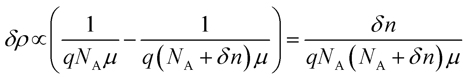 , where μ is the effective mobility of charge carriers. When δn is less than the doping density NA, the resistivity modulation is nearly linearly proportional to the excess carrier density (δn). However, when δn exceeds the doping density NA, the resistivity modulation depends less on the excess carrier density and becomes saturated.
This indicates that positive photocurrent (PPC) is observed when the optically induced voltage on the oxide layer and graphene surpasses the optically induced band bending. Conversely, negative photocurrent (NPC) is observed otherwise.
4. Conclusion
In conclusion, graphene–insulator–silicon (GIS) photodetectors demonstrate high sensitivity owing to their unique majority carrier type device characteristics, characterized by a lower Schottky barrier height (SBH) compared to half of the energy band gap in the active semiconductor. The primary factors contributing to the photoinduced SBH variation in GIS photodetectors are the photoinduced band bending, graphene Fermi level shift, and oxide voltage enhancement. These variations enable GIS devices to function as giant amplifiers, with the interplay among band bending, oxide voltage, and graphene Fermi level contingent upon the optical power, bias voltage, and wavelength of the illuminating light. Consequently, the photocurrent switches from positive photocurrent (PPC) to negative photocurrent (NPC) as optical power decreases, with the transition from positive photoresponsivity (PPR) to negative photoresponsivity (NPR) occurring below a critical optical power, dependent also on the reverse bias voltage. This transition mechanism is universally applicable to graphene–insulator–silicon photodetectors.The study unequivocally showcases that MC-GIS photodetectors exhibit exceptional sensitivity to low optical power levels, making them promising for detecting such signals and underscoring their potential for advanced applications such as single-photon detection in emerging fields like autonomous vehicles, quantum telecommunications, and photonic quantum computing. MC-GIS photodetectors hold promising prospects for advancing research in these areas.
5. Experimental section
Graphene synthesis
Large-area graphene layers were synthesized using the chemical vapor deposition (CVD) method on a copper (Cu) foil catalyst.22–26 The process involved etching a Cu foil with FeCl3 solution after depositing a polymethyl methacrylate (PMMA) layer on the graphene/Cu layers. To eliminate any residues on the graphene surface, the PMMA/graphene layer underwent multiple cleaning steps using deionized (DI) water.22–26MC-GIS device fabrication
GIS device fabrication: the device fabrication procedure for MC-GIS photodetectors is schematically depicted in Fig. S1a (ESI†). Initially, a gold (Au) layer was deposited onto the silicon substrate as the back contact using a sputtering system. Additionally, two aluminum (Al) electrodes were formed onto the SiO2/Si(100) wafer. The resistivity of the silicon substrate used in the fabrication process is 1–10 Ω cm. The distance between the deposited aluminum (Al) electrodes was 4 mm. Following the photolithography process for the silicon window opening, a partial area of SiO2 with a thickness of 300 nm (2 mm × 2 mm) was etched using a buffered oxide etch (BOE) solution. Subsequently, the silicon window was exposed to air for a duration of 1000 minutes to allow for the formation of an optimum thickness of the oxide layer, as reported in a previous study.23 Finally, the PMMA/graphene layer was transferred onto both the exposed silicon and the two Al electrodes. To remove any remaining moisture, the fabricated MC-GIS photodetector was left at room temperature for 30 minutes. Subsequently, the GIS device was loaded into a vacuum chamber and annealed at 180 °C for 30 minutes to ensure proper adhesion and stability.Characterizations
The current–voltage (I–V) characteristics were measured using a Keithley 6430 source meter. For the measurements, an aperture mask with an opening window area of 2 mm × 2 mm, which corresponds to the area of the graphene–silicon junction window, was placed on the MC-GIS photodetector The photocurrent behavior of the MC-GIS photodetectors was measured under different optical powers, ranging from 8.32 nW to 0.3 mW, using LEDs with wavelengths of 640 nm and 532 nm from Mightex Systems. The measurements were conducted in the reverse bias voltage region, spanning from 0 V to −5 V with a step size of 0.1 V. The LED lights were directed onto the graphene–silicon junction area using an aperture mask of the same size as the junction window area. To study the dark current behavior of the GIS device, measurements were performed before and after illumination with 640 nm and 532 nm LED lights. The dark current was measured in the voltage range of −5 V to 3 V, both before and after illumination.Capacitance–voltage (C–V) characteristics were measured using an HP 4192 A LF impedance analyzer. The C–V curves were obtained at different illumination states, including dark and various optical power levels (2.29 μW, 4.57 μW, 43.5 μW, and 0.1 mW), using a red LED. The measurements were performed at a modulation frequency of 1 kHz.22,37
Conflicts of interest
There are no conflicts to declare.Acknowledgements
This research was supported by Basic Science Research Program through the National Research Foundation of Korea (NRF) funded by the Ministry of Education (NRF-2019R1F1A1063643 and BK21 FOUR Program). All graphs were plotted by Igor Pro 8. Received: ((will be filled in by the editorial staff)) Revised: ((will be filled in by the editorial staff)) Published online: ((will be filled in by the editorial staff)).References
- J. Wu, Y. Guo, C. Deng, A. Zhang, H. Qiao, Z. Lu, J. Xie, L. Fang and Q. Dai, Nature, 2022, 612, 62 CrossRef CAS PubMed.
- W. Yang, J. Chen, Y. Zhang, Y. Zhang, J.-H. He and X. Fang, Adv. Funct. Mater., 2019, 29, 1808182 CrossRef.
- O. Gietelink, J. Ploeg, D. Schutter and M. Verhaegen, Veh. Syst. Dyn., 2006, 44, 569 CrossRef.
- N. Li, C. P. Ho, J. Xue, L. W. Lim, G. Chen, Y. H. Fu and L. Y. T. Lee, Laser Photonics Rev., 2022, 16, 2100511 CrossRef.
- Z. Zhang, F. Wen, Z. Sun, X. Guo, T. He and C. Lee, Adv. Intell. Syst., 2022, 4, 2100228 CrossRef.
- Q. Chi, H. Yan, C. Zhang, Z. Pang and L. D. Xu, IEEE Trans. Ind. Informatics, 2014, 10, 1417 Search PubMed.
- S. Yanikgonul, V. Leong, J. R. Ong, T. Hu, S. Y. Siew, C. E. Png and L. Krivitsky, Nat. Commun., 2021, 12, 1834 CrossRef CAS PubMed.
- D. Liu, T. Li, B. Tang, P. Zhang, W. Wang, M. Liu and Z. Li, Micromachines, 2022, 13, 47 CrossRef PubMed.
- A. Rochas, M. Gani, B. Furrer, P. A. Besse, R. S. Popovic, G. Ribordy and N. Gisin, Rev. Sci. Instrum., 2003, 74, 3263 CrossRef CAS.
- B. Wang and J. Mu, PhotoniX, 2022, 3, 8 CrossRef.
- S. Töpfer, M. G. Basset, J. Fuenzalida, F. Steinlechner, J. P. Torres and M. Gräfe, Sci. Adv., 2022, 8, eabl4301 CrossRef PubMed.
- C. Liu, J. Guo, L. Yu, J. Li, M. Zhang, H. Li, Y. Shi and D. Dai, Light: Sci. Appl., 2021, 10, 123 CrossRef CAS PubMed.
- K. S. Novoselov, A. K. Geim, S. V. Morozov, D. Jiang, Y. Zhang, S. V. Dubonos, I. V. Grigorieva and A. A. Firsov, Science, 2004, 306, 666 CrossRef CAS PubMed.
- K. S. Novoselov, A. K. Geim, S. V. Morozov, D. Jiang, M. I. Katsnelson, I. V. Grigorieva, S. V. Dubonos and A. A. Firsov, Nature, 2005, 438, 197 CrossRef CAS PubMed.
- A. H. Castro Neto, F. Guinea, N. M. R. Peres, K. S. Novoselov and A. K. Geim, Rev. Mod. Phys., 2009, 81, 109 CrossRef CAS.
- R. R. Nair, P. Blake, A. N. Grigorenko, K. S. Novoselov, T. J. Booth, T. Stauber, N. M. R. Peres and A. K. Geim, Science, 2008, 320, 1308 CrossRef CAS PubMed.
- X. An, F. Liu, Y. J. Jung and S. Kar, Nano Lett., 2013, 13, 909 CrossRef CAS PubMed.
- A. Di Bartolomeo, Phys. Rep., 2016, 606, 1 CrossRef.
- F. H. L. Koppens, T. Mueller, P. Avouris, A. C. Ferrari, M. S. Vitiello and M. Polini, Nat. Nanotechnol., 2014, 9, 780 CrossRef CAS PubMed.
- A. Pelella, A. Grillo, E. Faella, G. Luongo, M. B. Askari and A. D. Bartolomeo, ACS Appl. Mater. Interfaces, 2021, 13(40), 47895–47903 CrossRef CAS PubMed.
- A. D. Bartolomeo, G. Luongo, F. Giubileo, N. Funicello, G. Niu, T. Schroeder, M. Lisker and G. Lupina, 2D Mater., 2017, 4, 025075 CrossRef.
- H. K. Park and J. Choi, ACS Photonics, 2018, 5, 2895 CrossRef CAS.
- H. K. Park and J. Choi, J. Mater. Chem. C, 2018, 6, 6958 RSC.
- H. K. Park, Y. Cho, M. Kim and J. Choi, J. Mater. Chem. C, 2019, 7, 9346 RSC.
- Y. Cho, H. Kim and J. Choi, Adv. Opt. Mater., 2022, 10, 2200454 CrossRef CAS.
- M. A. Green, V. A. K. Temple and J. Shewchun, Solid-State Electron., 1975, 18, 745 CrossRef CAS.
- M. A. Green and J. Shewchun, Solid-State Electron., 1974, 17, 349 CrossRef CAS.
- S. M. Sze and K. K. Ng, Physics of Semiconductor Devices, John Wiley & Sons, Inc., Hoboken, NJ, USA, 3rd edn, 2007 Search PubMed.
- A. A. Abdou and S. E. D. Habib, Solid-State Electron., 1986, 29, 751 CrossRef CAS.
- N. K. Tailor, C. A. Aranda, M. Saliba and S. Satapathi, ACS Mater. Lett., 2022, 4(11), 2298–2320 CrossRef CAS.
- H. J. Kim, Khang J. Lee, J. Park, G. H. Shin, H. Park, K. Yu and S.-Y. Choi, ACS Appl. Mater. Interfaces, 2020, 12(34), 38563–38569 CrossRef CAS PubMed.
- P.-F. Wang, Y. Liu, J. Yin, W. Ma, Z. Dong, W. Zhang, J.-L. Zhu and J.-L. Sun, J. Mater. Chem. C, 2019, 7, 887–896 RSC.
- C. Biswas, F. Güneş, D. D. Loc, S. C. Lim, M. S. Jeong, D. Pribat and Y. H. Lee, Nano Lett., 2011, 11, 4682–4687 CrossRef CAS PubMed.
- E. Baek, T. Rim, J. Schütt, C. Baek, K. Kim, L. Baraban and G. Cuniberti, Nano Lett., 2017, 17(11), 6727–6734 CrossRef CAS PubMed.
- J. R. Barrett and G. C. Gerhard, J. Appl. Phys., 1967, 38, 900–902 CrossRef CAS.
- C. M. Penchina, J. S. Moore and N. Holonyak, Jr., Phys. Rev., 1966, 143, 634 CrossRef CAS.
- H. K. Park and J. Choi, Adv. Electron. Mater., 2018, 4, 1700317 CrossRef.
Footnote |
| † Electronic supplementary information (ESI) available: Fabrication process of GIS photodiodes and experimental set-up for photo-response studies (S1), photo-capacitance (S2) and photo current–voltage (I–V) characteristics and Schottky barrier height modulation under light illumination (S3) are included in Supplementary Information in detail. See DOI: https://doi.org/10.1039/d4tc00664j |
| This journal is © The Royal Society of Chemistry 2024 |