
 Open Access Article
 This Open Access Article is licensed under a Creative Commons Attribution-Non Commercial 3.0 Unported Licence
High quality MAPbBr3 films via pulsed laser deposition of single-crystalline targets†
E.
Ghavidel
ab,
A.
Di Carlo
 ab,
A.
Ishteev
ce,
J.
Barichello
a,
K.
Konstantinova
c,
D.
Saranin
c,
V.
Campanari
a,
F.
Martelli
d,
B.
Paci
a,
A.
Generosi
a,
M.
Guaragno
a,
A.
Cricenti
a,
D.
Becerrill
a,
M.
Luce
a,
F.
Matteocci
b and
A.
Di Trolio
*a
ab,
A.
Ishteev
ce,
J.
Barichello
a,
K.
Konstantinova
c,
D.
Saranin
c,
V.
Campanari
a,
F.
Martelli
d,
B.
Paci
a,
A.
Generosi
a,
M.
Guaragno
a,
A.
Cricenti
a,
D.
Becerrill
a,
M.
Luce
a,
F.
Matteocci
b and
A.
Di Trolio
*a
aCNR – Istituto di Struttura della Materia, Via del Fosso del Cavaliere 100, 00133 Roma, Italy. E-mail: antonio.ditrolio@cnr.it
bCHOSE – Dept. Electronic Engineering University of Rome Tor Vergata, via del Politecnico 1, 00133 Rome, Italy
cLASE – Laboratory of Advanced Solar Energy, NUST MISiS, 119049 Moscow, Russia
dCNR – Istituto per la microelettronica e microsistemi, Via del Fosso del Cavaliere 100, 00133 Roma, Italy
eN.N. Semenov Federal Research Center for Chemical Physics, Russian Academy of Sciences, 119991 Moscow, Russia
First published on 15th July 2024
Abstract
High quality MAPbBr3 films were grown by pulsed laser deposition of single-crystalline targets using an on-axis geometry. The gas ambience up to the mbar range and laser fluence of some tenths of Joule per square centimeter yielded single α-phase polycrystalline MAPbBr3 films, as revealed by ex situ XRD analysis. In situ low T studies allowed for the observation of cubic-to-tetragonal and of tetragonal-to-orthorombic phase transitions. Absorption and photoluminescence spectra show characteristic peaks around 2.35 eV. In particular, for thin films, PL measurements at low temperature showed narrow peaks characteristic of high crystalline quality and the absence of relevant defect-related recombination. The present results indicate a route to grow high quality thin films of metal halide perovskites via PLD of single-crystalline targets.
1. Introduction
In the last decade, much attention has been paid to hybrid organic–inorganic lead halide perovskites for the possibility to realize photovoltaic devices with efficiency larger than 25%. However, the realization of high-quality devices is quite difficult because the perovskite family is unstable under the effects of temperature, humidity and light. Moreover, most of the high-performance absorber layers have been grown by solution processing techniques which could present drawbacks due either to a high defect concentration or to the residual presence of the solvent traces in the film.1–5To overcome such inconvenience, full dry growth processes proved to be successful for materials based on metal oxides have been explored.6 Among these, the versatile pulsed laser deposition (PLD) permits us to grow layers in a wide range of parameter values, starting from a single stoichiometric target. Here, the stoichiometry preservation from the target to film allows the growth of films as pure as the single crystals up to large-area coatings on a variety of substrates, including flexible materials. However, the presence in hybrid perovskites of elements with a significant difference in atomic weight makes the stoichiometry transfer from the target to the substrate difficult. This is due to the collisions of the plasma constituents among themselves or with the background gas particles leading to an incongruent ablation process with non-stoichiometric transfer of materials on the substrate, mainly consisting of the brownish PbX2 phase.7–9 Indeed, the lighter plasma constituents are preferentially scattered and diffused to larger angles resulting in an enhancement of the heavier species along the direction normal to the substrate.7–9 MAPbX3 layers have been deposited by PLD at low laser fluence, mainly ablating off-stoichiometric targets with a MAX![[thin space (1/6-em)]](https://www.rsc.org/images/entities/char_2009.gif) :PbX2 molar ratio higher than 4 to balance the stoichiometry losses due to the scattering of organic species during deposition.10–14 Both for hybrid organic–inorganic lead halide and for inorganic15,16 and lead-free perovskites,17,18 the PLD experiments were mainly performed with KrF excimer lasers operating at 248 nm. The use of excimer lasers raises safety concerns, as they contain highly poisonous gases, necessitating for expensive infrastructure to ensure safety. Additionally, the increasing demand for noble gases and their limited availability have led to a significant increase in the cost of the KrF premix gas mixture in recent years.
:PbX2 molar ratio higher than 4 to balance the stoichiometry losses due to the scattering of organic species during deposition.10–14 Both for hybrid organic–inorganic lead halide and for inorganic15,16 and lead-free perovskites,17,18 the PLD experiments were mainly performed with KrF excimer lasers operating at 248 nm. The use of excimer lasers raises safety concerns, as they contain highly poisonous gases, necessitating for expensive infrastructure to ensure safety. Additionally, the increasing demand for noble gases and their limited availability have led to a significant increase in the cost of the KrF premix gas mixture in recent years.
Nd:Yag lasers allow these safety issues to be overcome and, moreover, meet the needs of low energy for the growth of a volatile perovskite. In fact, the fundamental emission at 1064 nm and the higher harmonics at 532 and 355 nm, whose photon energies are lower than those of the KrF excimer lasers, make Nd–Yag lasers very suitable for the deposition of hybrid organic–inorganic lead halide perovskites.
In this paper, we report on the deposition of MAPbBr3 films by on-axis PLD of single stoichiometric targets. To preserve the stoichiometry in the deposition process, we minimized the kinetic energy of ions and neutral species of the plasma by decreasing either the laser fluence or increasing the gas pressure in the growth chamber. Moreover, by ablating single-crystal stoichiometric targets, films with excellent structural and optical properties were deposited.
2. Experimental section
The organic–inorganic hybrid perovskite films were deposited by on-axis PLD using a Nd:YAG laser, operating at λ = 355 nm and a 10 Hz repetition rate, starting from a single crystal target (Fig. 1). The commercial ITO/glass substrate was kept at 100 °C during the deposition, which takes place in the presence of Ar. To improve homogeneous covering of the substrates, the deposition process was carried out by scanning an area of 2.5 × 2.5 cm2, by a computer-controlled substrate motion, allowing substrate displacements in the plane perpendicular to the direction of plume expansion. By variation of motion velocity and the duration at each single deposition-point, the full coverage of the substrates was ensured as well as the deposition time and film thickness control. To improve film quality, several attempts have been made by controlling various parameters like Ar pressure in the chamber, laser fluence, and the substrate to target distance. The optimal growth conditions were achieved at a laser fluence of 0.2 J cm−2, a spot size of 0.03 cm2, an Ar background pressure of 0.7–1 mbar, and a target to substrate distance of 5 cm. The duration of the deposition process is 4 min for a film thickness of about 100 nm. | ||
| Fig. 1 (A) Schematic of the PLD technique, (B) XRD pattern of the single-crystal before (red line) and after (gray line) grinding, and (C) single-crystal target of MAPbBr3. | ||
The MAPbBr3 single crystal, used as a target source, was synthesized utilizing an inverse temperature solubility technique. In a nitrogen-filled glovebox, an equimolar mixture of methylammonium bromide (CH3NH3Br, 224 mg, 2 mmol) and lead(II) bromide (PbBr2, 734 mg, 2 mmol) was dissolved in anhydrous dimethylformamide (DMF, 2 mL). The resultant mixture was magnetically stirred overnight at 25 °C to ensure complete dissolution of the salts. The resulting solution was subjected to a thorough filtration to achieve a solution devoid of particulate matter. To inhibit uncontrolled nucleation, glass vials intended for crystal growth were treated with dimethyldimethoxysilane to render the inner surfaces hydrophobic, thereby increasing the wetting angle between the glass and the DMF solution. For the nucleation phase, a diminutive seed crystal of MAPbBr3, with dimensions typically less than 1 mm3, was delicately placed at the bottom of the pre-treated vial. The vial containing the seed crystal and the precursor solution was then situated atop a heating plate. The temperature was increased at a gradual rate of 8 °C hour−1 from an initial temperature of 68 °C to 78 °C. This temperature was maintained until the onset of crystal growth was observed. Thereafter, the heating rate was diminished to 8 °C hour−1 until the temperature reached 90 °C. Throughout the growth period, the assembly was positioned on an anti-vibration marble balance table to mitigate any external disturbances that could affect crystal integrity. The vials were capped with glass lids to prevent heat loss. The resulting crystals exhibited a cubic morphology and reached a final size of 6 × 6 × 3 mm. Optical characterization was performed using a UV-Vis spectrophotometer, a Shimadzu MPC 2600, in the absorbance mode. A Panalytical Empyrean X-ray diffractometer was used to collect diffraction patterns (XRD) in the Bragg–Brentano configuration. Detection was accomplished by means of a PixCel 3D detector working in linear mode and a Cu-anode X-ray tube (K-Alpha1 [Å] = 1.54060; K-Alpha2 [Å] = 1.54443) was used as a source. Divergent slits (slit size [°] = 0.2177) set the incident optical pathway and structural information was collected in the 5° < 2θ < 70° angular range (step size [°2θ] = 0.0260, scan step time [s] = 1145, scan type continuous). Samples were located onto a flat sample holder and generator parameters were kept fixed at 45 mA and 40 kV. For phase transition low temperature measurements, the instrumentation was equipped with a Linkam hot-cold temperature-controlled stage (THMS600), properly modified to fit the peculiar demands of this experiment. A controlled atmosphere was set by means of a constant N2 flux within the cell, whose temperature was varied in the 83 K < T < 293 K range, with steps of 10–20 K. At each temperature, a rapid XRD pattern was collected in the 16° < 2θ < 40° angular range, suitable to track any possible structural modifications as well as to optimize the requirements for a fast collection to be achieved (step size [°2θ] = 0.0260; scan step time [s] = 46.6650).
An in-house developed atomic force microscope (AFM) mounted with a 30 μm × 30 μm scanner was used in non-contact mode to determine the surface morphology of the various samples. It works by means of aluminum coated standard tapping AFM probes (Nanosensors), combining high operation stability with outstanding sensitivity and fast scanning ability.
Energy-dispersive X-ray reflectometry measurements (EDXR) were performed by means of a non-commercial, in-house patented reflectometer in order to study the morphological characteristics of the layered samples, i.e., thickness and surface/interface roughness. The whole white beam produced using a W-anode X-ray lamp (10–50 keV) is focused onto the sample by means of micrometric W-slits (20 × 20 μm square aperture) and the reflected signal is detected by a Ge-single crystal detector which is able not only to count the incoming photons but also to discriminate their energy. The geometry of the experimental apparatus is kept fixed during the measurements, no angular movement being required and pattern acquisition occurs simultaneously in the whole explored energy-range.
X-ray photoelectron spectra (XPS) were recorded in a Vacuum Generators VG-450 ultrahigh-vacuum chamber equipped with an Al Kα radiation source with an estimated resolution of 0.1 eV. The C1s spectra of adventitious carbon were used as a reference to discard any possible charging effects. Spectra were fit using pseudo-Voigt models and the contributions of each oxidation state were calculated from the cover of the curves.
Steady-state photoluminescence (PL) measurements were performed in the temperature range 12 ≤ T ≤ 293 K using a cw laser diode emitting at 405 nm. The PL was dispersed by a 30-cm spectrometer and revealed by a Peltier-cooled CCD camera.
Cell fabrication
A Nd:YVO4-pulsed UV laser system (BrightSolutions, Luce 40 laser) has been utilized to etch square-shaped (2.5 × 2.5 cm2) Pilkington FTO substrates (7 Ω □−1). Then, substrates underwent a thorough cleaning process to remove contaminants: a mechanical washing with a soap solution (2% Hellmanex in water) for organic residue and dust removal; ultrasonic baths in distilled water and isopropanol (40 °C, 10 minutes each) for further cleaning and finally a UV/O3 treatment with a PSD Pro Series Digital UV Ozone System (Novascan) for 15 minutes to eliminate remaining organic materials. The compact TiO2 as electron transport layer (ETL) has been deposited through the spray pyrolysis technique. The ETL deposition occurred through air as the gas carrier at a pressure of 1.6 bar and a nozzle angle of about 45°, with 8–10 spray cycles (once every 10 seconds) once the hot plate reached 465 °C. After the spray pyrolysis, substrates were maintained at 465 °C for 10 minutes and then the temperature was decreased.10 mg mL−1 of PTAA powder (10 KDa) was dissolved in toluene and before deposition doped with 4-tert-butylpyridine (10 μL mL−1) and LiTFSI (5 μL mL−1 from a stock solution of 170 mg mL−1 in acetonitrile). The PTAA layer was spin coated at 4000 rpm for 20 seconds. Transparent conductive indium tin oxide (ITO) as a top electrode was deposited by a low temperature sputtering process at 1.1 × 10⁻³ mbar and a 60 W RF power. During the ITO deposition, inert Ar gas was purged in the chamber (40 sccm) to activate the Ar+ plasma. The sample holder was moved below the ITO cathode with a speed of 120 cm min−1 for 300 cycles to achieve a thickness of 100–120 nm.
PV parameter characterization
J–V curves and PV parameters of devices were detected using a Class-A Sun Simulator (ABET 2000) furnished with an AM1.5G filter (ABET). For calibrating the sun simulator, a Si-based reference cell (RR-226-O, RERA Solutions) was utilized. Arkeo platform (Cicci Research S.r.l.) was used for J–V data acquisition in forward and reverse voltage scan modes, using a voltage step of 20 mV s−1 and a voltage scan rate of 200 mV s−1.3. Discussion
The deposition parameters of the PLD were selected after depositing MAPbBr3 undre the typical conditions of 1 J cm−2, 10−5 mbar of Ar, and 100 °C. Such films looked brownish due to PbBr2 phase and the minority presence of α-phase was detected. Subsequently, by reducing the fluence and increasing the Ar pressure, the presence of the MAPbBr3 phase gradually increases with respect to PbBr2 and, when the fluence is less than 0.5 J cm−2 and the Ar pressure approaches 1 mbar, the MAPbBr3 α-phase becomes predominant. The optimal values of fluence and Ar pressure, at which the single α-phase films are grown, are of 0.2 J cm−2 and 0.7 mbar, respectively.The surface texture of the samples is quite uniform (i.e., without specific defects or agglomerates) as shown in Fig. 2a for a thin film with a thickness of about 100 nm. No significant roughness (r.m.s.) variation is observed comparing smaller (10 μm × 10 μm) and larger (30 μm × 30 μm) AFM images (see Fig. S1, in the ESI†). However, the roughness values are quite relevant, within the 9–14 nm range, independently of the image size and the texture is characterized by compact spherical grains all over the probed surface (Fig. 2a).
 | ||
| Fig. 2 (a) AFM image of thin MAPbBr3 film growth via PLD at 1 mbar of Ar pressure on a region of 20 × 20 μm2 (b) and EDXR profiles collected at 0.210° upon two MAPbBr3 samples. (c) XRD patterns of MAPbBr3 films grown at a fluence of 0.2 J cm−2 and an Ar pressure of 0.02 (blue line) and 1 mbar (black line). | ||
Such elevated roughness is confirmed by EDXR measurements: in the patterns reported in Fig. 2b no Kiessig fringes are visible due to high surface/interface roughness of the samples, as indicated by the sharp slope of the curves and in good agreement with AFM. Additionally, the reflectivity edge at qc = 0.041 A−1 allowed evaluating the perovskite (PVK) electron density to be ρe = 3.34 (1) × 10−5 A−2 in good agreement with the literature.19
The role of the Ar pressure in the deposition is evident from the XRD spectra of MAPbBr3 films reported in Fig. 2c and d. Although the films were grown at a fluence of 0.2 J cm−2, the spectra of the films deposited at an Ar pressure of 0.02 (c) and 1 mbar (d) are quite dissimilar. No PVK crystalline signature is detected in the first case, and the visible reflections arise only from the TCO substrate and PbBr2 (Fig. 2c blue line, reflections labelled with a star *). These reflections were assigned according to JCDD card no: 001-0625 and JCDD card no: 031-0679, respectively. In the last case, a polycrystalline structure results with Miller indexes assigned to the MAPbBr3 α-phase (Fig. 2b).20 Indeed, the perovskite adopted a cubic Pm![[3 with combining macron]](https://www.rsc.org/images/entities/char_0033_0304.gif) m polycrystalline structure at room temperature, the reflections being labelled according to literature.5,20,21 The transparent conductive oxide (TCO) is labelled according to ICDD card no. 001-0625 and can be referred to as the substrate.
m polycrystalline structure at room temperature, the reflections being labelled according to literature.5,20,21 The transparent conductive oxide (TCO) is labelled according to ICDD card no. 001-0625 and can be referred to as the substrate.
The MAPbBr3 film is also stable in nitrogen storage as revealed by the XRD patterns collected for the stored sample (25 days) perfectly matching with the as-deposited film pattern, reported in Fig. S2, ESI.† The structural stability of the MAPbBr3 films was investigated as a function of temperature. Starting from room temperature (RT), the structural modifications have been monitored by means of temperature-dependent XRD measurements down to 78 K. Fig. 3a shows the XRD patterns of the film measured in the 293–78 K temperature range: XRD patterns collected by means of the hot cold Linkam cell are shown together with a highlight of the PVK reflections. PVK reflections attributed to the (200) and (110) crystal planes were fitted by means of Gaussian function to monitor their crystallinity, position and grain size evolution as a function of temperature. The film structure is preserved down to 230 K, then phase transitions occur at temperatures in between 233–223 K, 163–153 K and ≈ 113K corresponding to structural changes from cubic Pmm (α-PVK) to tetragonal I4/mcm (β-PVK), from tetragonal to orthorhombic I Pna21 and finally to orthorhombic II Pnma (δ-PVK), respectively. In Fig. 3b, these observations are reported as a function of peak position along the (200) plane, and a sudden lattice contraction corresponds to phase transitions.22,23
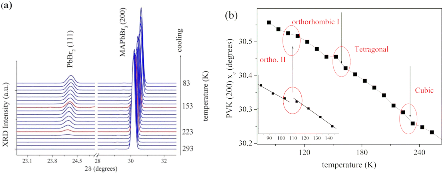 | ||
| Fig. 3 (a) Temperature dependent XRD patterns collected cooling down the MAPbBr3 film from 293 K to 78 K. PVK reflections are labelled with Miller indexes identifying each reflection; (b) compression of MaPbBr3 lattice parameters along the (200) crystallographic direction as a function of temperature. Phase transitions are evidenced. | ||
Furthermore, it was possible to detect other structural modifications during the cooling process triggered by the structural rearrangements related to the MAPbBr3 phase transitions. Indeed, as the cubic to tetragonal PVK phase transition takes place at 223–233 K, the sudden formation of PbBr2 is observed, with the (020)-(111)-(102) peaks being clearly detected [JCDD card nr: 00-001-0623]. The temperature dependent evolution of its structural parameters is reported in Fig. S3 of the ESI,† with the trend of the (020) reflection being representative of the whole PbBr2 behavior.
As visible, in analogy to what is observed for the PVK lattice, lowering the temperature the lead bromide lattice contracts. The crystallinity evolution evidences two distinct processes:
(1) Primary crystallization: crystallinity increases and the grain size diminishes due to the formation of novel small crystallites up to 173 K.
(2) Secondary crystallization (at lower temperatures): both reflection intensity and grain size increase. This latter process is due to enlargement of previously existing small crystallites, merging into larger ones, amorphous lead bromide still crystallizing by nucleation of pre-existing crystallites.
It is worth noticing that phase transition at low temperatures triggers the formation of the PbBr2 phase, typically associated with the perovskite decomposition triggered by light, high temperature, pressure, humidity and many other conditions.24,25 As shown in Fig. S4 of the ESI,† the PbBr2 formation is not reversible, the reflection still being present after the whole thermal cycle, however this presence does not affect the overall perovskite crystallinity and phases, which are perfectly reversible, as expected for high quality, stable MAPbBr3 films, proving that the thermodynamical properties of the material are preserved and that the alpha phase is stable and optimized (as for chemical deposition methods) as required for photovoltaic applications, fully validating the PLD technique.
The possible presence at RT of amorphous PbBr2 in the films has been investigated by performing X-ray photoelectron spectroscopy (XPS). Fig. 4 shows a typical spectrum of the thin film grown from a single crystal target with only two peaks corresponding to the Pb 4f5/2 and Pb 4f7/2 electrons. The peak positions and hence the Pb–Br charge transfer rule out the presence of amorphous PbBr2, within the measurement error of 2%. Moreover, the comparison of the XPS spectra with those of a control sample, reported in Fig. S5 of the ESI,† indicates the only presence of the PbBr3 phase, as it results from the data analysis reported in Table 1.
 | ||
| Fig. 4 A typical XPS spectrum of a thin MAPbBr3 film grown from a single crystal target under the optimal growth conditions. | ||
| Pb 4f 5/2 | Pb 4f 7/2 | |
|---|---|---|
| Center (eV) | 142.6 | 137.8 |
| FWHM (eV) | 1.1 | 1.1 |
| Contribution (%) | 40.9 | 59.1 |
Also based on the XRD results, the XPS data analysis suggests that only the MAPbBr3 phase is present in the film. As a consequence, the material transfer from the crystal target of only the MAPbBr3 phase (see Fig. 1b) to the film, under the experimental conditions of high background gas pressure and low laser fluence, is stoichiometric. The presence of PbBr2 is however detected in the single crystal target after cumulative depositions, as shown in the XPS spectrum reported in Fig. S5 of the ESI.† An equivalent amount of PbBr2 and PbBr3 phases was found on the sample surface by fitting with four peaks the spectra corresponding to Pb 4f electrons of the PbBr2 and PbBr3 phases. A binding energy difference of 4.8 eV between the doublets of both crystals was confirmed and an increase in binding energy of 2.4 eV was found between PbBr2 and PbBr3. The fitting parameters can also be found in Table S1 of the ESI.†
For optical characterization, absorption and photoluminescence spectra were obtained and compared. The absorption spectra show enhanced absorption in the visible range between 400 and 600 nm with excitonic peaks of the MAPbBr3 phase between 510 and 520 nm (2.33 and 2.43 eV), see Fig. 5a.
 | ||
| Fig. 5 (a) Absorption spectra of MAPbBr3 films grown at different Ar pressures showing the evolution of the characteristic peak. (b) PL spectra for different laser power values. The laser power of 10 μW corresponds to an excitation density of about 1 kW m−2 close to a density power of 1 sun. (c) PL intensity as a function of excitation power and (d) PL spectra as a function of temperature between 12 and 290 K. | ||
The role of the Ar pressure in the deposition is evident from the absorption spectra of samples deposited at a low fluence (0.2 J cm−2) under different gas ambient conditions. The samples grown at 10−6 mbar do not exhibit peaks and the excitonic peak of MAPbBr3 appears at ∼520 nm only as the Ar pressure increases up to values in the [10−1–1] mbar range.
The PL spectra of a thin sample (100 nm) measured at 12 K as a function of the excitation power are reported in Fig. 5b. The highest excitation power used is equivalent to about 100 sun with the lowest value being about 10−4 sun. Two important aspects can be extracted from the PL spectra at 12 K. The first one is that the intensity of the emission at energy below the excitonic one is very weak, barely visible only at the lowest excitation density. An excitation of about 10−3 sun already shows the saturation of defect-related signals. This is a clear indication of the superior optical and structural quality of our samples. The second aspect is that the dependence of the PL intensity on the excitation density is almost linear (see Fig. 5c) demonstrating the excitonic-like character of the signal. The linearity at low excitations is also a further indication of the low defect density present in the samples. We have to report that the increase of the film thickness results in a stronger emission from defect-related recombination (see Fig. S6 of the ESI†). We also compared the optical qualitity of thin films grown from pellets and from single crystal targets with that of the single crystal. The PL energy of the single crystal lies at energies slightly below that of the two thin films (see Fig. S7 in the ESI†). This is due to the high density of defects present in the single crystals, as also testified by the presence of a low-energy shoulder in the relative spectrum. These PL results further confirm the stoichiometric transfer from the crystal to the film.
Finally, the temperature dependence of the PL is shown in Fig. 5d. The PL peak smoothly blue-shifts as the temperature is increased and no evidence for effects of the phase transitions on the PL energy is observed. The PL spectra of MAPbBr3 films of thickness lower than 100 nm differ from those reported for single crystals5 and nanosheets of MAPbBr3,26 where more peaks are present at RT. The difference between samples of different origins is likely due to density and type of the structural defects that form during the different growths. The presence of a single, excitonic, peak in the PL spectra of our samples is a further indication of the superior quality of our thinner films.
Finally, we prepared a semitransparent MAPbBr3-based device depositing a perovskite layer of 300 nm by PLD on FTO-glass/TiO2 substrates, and obtaining a structure with PTAA (poly[bis(4-phenyl)(2,4,6-trimethylphenyl)amine]) and ITO (indium tin oxide) layers. Current density (J) vs. voltage (V) characteristics are shown in Fig. 6a together with a photograph of the semitransparent cells. The external quantum efficiency together with the integrated short circuit J are shown in Fig. 6b. The photovoltaic parameters extracted from the JV characteristics are shown in Table 2. The efficiency of the cell, around 0.7%, needs to be compared with that of a semitransparent solution process-deposited MAPbBr3-based PSC that without post-treatments can achieve a performance of around 5%.27 The lower efficiency of MAPbBr3-based PLD cells compared to that of the solution processed or to the MAPbI3-based cells14,28 suggests that thickness and homogeneity coverage of the perovskite layer should be optimized to increase the VOC and PCE values towards 1.5 V and 7%, respectively.2,29–32 The excellent optical quality of the thinner films suggests that the major efforts to improve the device performance consist of a better control of the growth process as the growth time increases. The preliminary results shown here indicate that the potential of PLD for perovskite growth is high and could be exploited in application where conformability to the substrate is important such as for example the case of perovskite/silicon tandem solar cells.33
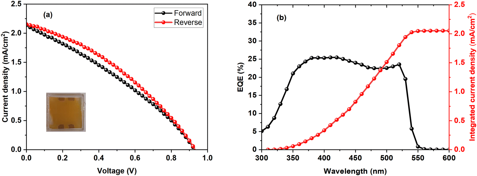 | ||
| Fig. 6 MAPbBr3-based semitransparent device FTO-glass/TiO2/MAPbBr3/PTAA/ITO: (a) forward and reverse J–V characteristics (inset: photograph of the cell), (b) external quantum efficiency (EQE) and integrated current density. | ||
| Scan mode | V OC (V) | J SC (mA cm−2) | FF (%) | PCE (%) |
|---|---|---|---|---|
| Forward | 0.929 | 2.139 | 31.53 | 0.63 |
| Reverse | 0.931 | 2.154 | 35.33 | 0.71 |
4. Conclusions
Very high-quality perovskite films were successfully grown by on-axis PLD, at low laser fluence and from stoichiometric targets. By increasing the Ar pressure during the deposition up to values in the mbar range, we minimized the loss of stoichiometry due to light species scattering, allowing the growth of single α-phase MAPbBr3 films with an extremely low density of defects as indicated by low-temperature PL.The structural stability of the films, investigated as a function of the temperature, showed that the film structure is preserved down to 230 K, whereas structural transitions occur at temperatures in between 233–223 K and 163–153 K corresponding to structural changes from the cubic to tetragonal and from tetragonal to orthorhombic lattices. XRD and optical absorption spectra underline the role of the Ar pressure in the growth process. Photoluminescence measurements demonstrate the exciton-like character of the radiative recombination. The present results represent a first step towards the growth of high quality thin films via PLD of single-crystalline targets.
Author contributions
ADC and ADT conceived the idea and planned the work. Perovskite film growth, ADT and EG; preparation and characterization of the solar cells, EG, JB, and FM,b; XRD and AFM characterization, BP, AG, and MG; photoluminescence measurements, FM4 and VC; single-crystal growth and characterization, AI, KK, and DS; XPS characterization, AC, DB, and ML; writing – original draft preparation, ADT; and writing – review and editing, ADC, BP, and FM,d. All authors discussed the results and commented on the manuscript.Data availability
The data supporting this study are available in the published article and in its ESI.†Conflicts of interest
There are no conflicts to declare.Acknowledgements
We are grateful to Massimiliano Latino for the technical support in the pulsed laser deposition experiments. The research was funded by EU H2020 Project “CITYSOLAR”–Grant agreement N.101007084- and by the national project CANVAS of the Ministero della Transizione Ecologica MiTE REGISTRO DECRETI.R.000182.05-08-2022. A. I., D. S., and K. K. gratefully acknowledge the financial support from the Ministry of Science and Higher Education of the Russian Federation in terms of the Program Priority 2030 in NUST MISIS (grant No. K2-2022-011).References
- F. Ye, H. Wu, M. Qin, S. Yang, G. Niu, X. Lu, J. Wang, D. B. Mitzi and W. C. H. Choy, ACS Appl. Mater. Interfaces, 2020, 12(21), 24498 CrossRef CAS PubMed
.
- W. Peng, L. Wang, B. Murali, K.-T. Ho, A. Bera, N. Cho, C.-F. Kang, V. M. Burlakov, J. Pan, L. Sinatra, C. Ma, W. Xu, D. Shi, E. Alarousu, A. Goriely, J.-H. He, O. F. Mohammed, T. Wu and O. M. Bakr, Solution-Grown Monocrystalline Hybrid Perovskite Films for Hole-Transporter-Free Solar Cells, Adv. Mater., 2016, 28, 3383 CrossRef CAS PubMed
- Z. Wang, M. Luo, Y. Liu, M. Li, M. Pi, J. Yang, Y. Chen, Z. Zhang, J. Du, D. Zhang, Z. Liu and S. Chen, Air-Processed MAPbBr3 Perovskite Thin Film with Ultrastability and Enhanced Amplified Spontaneous Emission, Small, 2021, 17, 2101107 CrossRef CAS PubMed
- L. Han, C. Liu, L. Wu and J. Zhang, Observation of the growth of MAPbBr3 single-crystalline thin film based on space-limited method, J. Cryst. Grow., 2018, 501, 27 CrossRef CAS
- K. H. Wang, L. C. Li and M. Shellaiah,
et al., Structural and Photophysical Properties of Methylammonium Lead Tribromide (MAPbBr3) Single Crystals, Sci. Rep., 2017, 7, 13643 CrossRef PubMed
- T. Soto-Montero, W. Soltanpoor and M. Morales-Masis, APL Mater., 2020, 8, 110903 CrossRef CAS
- S. Wicklein, A. Sambri, S. Amoruso, X. Wang, R. Bruzzese, A. Koehl and R. Dittmann, Pulsed laser ablation of complex oxides: The role of congruent ablation and preferential scattering for the film stoichiometry, Appl. Phys. Lett., 2012, 101, 131601 CrossRef
- A. Ojeda, C. W. Schneidera, M. Döbeli, T. Lipperta and A. Wokaun, The importance of pressure and mass ratios when depositingmulti-element oxide thin films by pulsed laser deposition, Appl. Surf. Sci., 2016, 389, 126–134 CrossRef
- P. R. Willmott and J. R. Huber, Pulsed laser vaporization and deposition, Rev. Mod. Phys., 2000, 72, 315 CrossRef CAS
- U. Bansode and S. Ogale, On-axis pulsed laser deposition of hybrid perovskite films for solar cell and broadband photo-sensor applications, J. Appl. Phys., 2017, 121(13), 133107 CrossRef
- U. Bansode, R. Naphade, O. Game, S. Agarkar and S. Ogale, Hybrid Perovskite Films by a New Variant of Pulsed Excimer Laser Deposition: A Room-Temperature Dry Process, J. Phys. Chem. C, 2015, 119, 9177–9185 CrossRef CAS
- T. Soto-Montero et al. , Single-Source Pulsed Laser Deposition of MAPbI3, IEEE 48th Photovoltaic Specialists Conference (PVSC), Fort Lauderdale, FL, USA, 2021, 1318–1323 DOI:10.1109/PVSC43889.2021.9518799.
- N. Patel, S. Dias and S. B. Krupanidhi, J. Electron. Mater., 2018, 4, 47 Search PubMed
- T. Soto-Montero, S. Kralj, W. Soltanpoor, J. S. Solomon, J. S. Gómez, K. P. S. Zanoni, A. Paliwal, H. J. Bolink, C. Baeumer, A. P. M. Kentgens and M. Morales-Masis, Single-Source Vapor-Deposition of MA1−xFAxPbI3 Perovskite Absorbers for Solar Cells, Adv. Funct. Mater., 2023, 2300588 CrossRef
- M. Cesaria, M. Mazzeo, G. Quarta, M. R. Aziz, C. Nobile, S. Carallo, M. Martino, L. Calcagnile and P. Caricato, Pulsed Laser Deposition of CsPbBr3 Films: Impact of the Composition of the Target and Mass Distribution in the Plasma Plume, Nanomaterials, 2021, 11, 3210 CrossRef CAS PubMed
- H. Wang, Y. Wu, M. Ma, S. Dong, Q. Li, J. Du, H. Zhang and Q. Xu, ACS Appl. Energy Mater., 2019, 2, 2305 CrossRef CAS
- N. Rodkey, S. Kaal, P. Sebastia-Luna, Y. A. Birkhölzer, M. Ledinsky, F. Palazon, H. J. Bolink and M. Morales-Masis, Chem. Mater., 2021, 33(18), 7417 CrossRef CAS PubMed
- V. M. Kiyek, Y. A. Birkhölzer, Y. Smirnov, M. Ledinsky, Z. Remes, J. Momand, B. J. Kooi, G. Koster, G. Rijnders and M. Morales-Masis, Adv. Mater. Interfaces, 2020, 7, 2000162 CrossRef CAS
- G. Bravetti, D. Altamura, B. Paci, A. Generosi, S. Carallo, M. Guaragno, G. Gigli, A. Listorti, G. Grancini, C. Giannini, S. Colella and A. Rizzo, Addressing the role of 2D domains in high-dimensionality Ruddlesden-Popper perovskite for solar cells, Sol. RRL, 2023, 7, 2200860 CrossRef CAS
- H. Shen, R. Nan and Z. Jian,
et al., Defect step controlled growth of perovskite MAPbBr3 single crystal, J. Mater. Sci., 2019, 54, 11596 CrossRef CAS
- C. Chen,
et al.
, J. Phys. D: Appl. Phys., 2018, 51, 045105 CrossRef
- V. Campanari, M. Lucci, L. Castriotta, B. Paci, A. Generosi, M. Guaragno, R. Francini, M. Cirillo and A. Di Carlo, Metal-Semiconductor Transition in Thin Film MAPbI3 Perovskite, Appl. Phys. Lett., 2020, 117, 261901 CrossRef CAS
- H. Abid, A. Trigui, A. Mlayah, E. K. Hlil and Y. Abid, Results Phys., 2012, 2, 71 CrossRef
- E. J. Juarez-Perez, L. K. Ono, M. Maeda, Y. Jiang, Z. Hawash and Y. Qi, Photodecomposition and thermal decomposition in methylammonium halide lead perovskites and inferred design principles to increase photovoltaic device stability, J. Mater. Chem. A, 2018, 6, 9604 RSC
- K.-H. Wang, L.-C. Li, M. Shellaiah and K. W. Sun, Structural and Photophysical Properties of Methylammonium Lead Tribromide (MAPbBr3) Single Crystals, Sci. Rep., 2017, 7, 13643 CrossRef PubMed
- D. Wang, W.-B. Shi, H. Jing, C. Yin, Y. Zhu, J. Su, G.-B. Ma, R. Peng, X. Wang and M. Wang, Opt. Express, 2018, 26, 27504 CrossRef CAS PubMed
- A. Singh, F. Matteocci, H. Zhu, D. Rossi, S. Mejaouri, S. Cacovich, M. Auf Der Maur, F. Sauvage, A. Gagliardi and M. Grätzel,
et al., Methylamine Gas Treatment Affords Improving Semitransparency, Efficiency, and Stability of CH3NH3PbBr3-Based Perovskite Solar Cells, Sol. RRL, 2021, 5, 2100277 CrossRef CAS
- W. A. Dunlap-Shohl, E. Tomas Barraza, A. Barrett, K. Gundogdu, A. D. Stiff-Roberts and D. B. Mitzi, MAPbI3 Solar Cells with Absorber Deposited by Resonant Infrared Matrix-Assisted Pulsed Laser Evaporation, ACS Energy Lett., 2018, 3, 270–275 CrossRef CAS
- J. H. Heo and D. H. Song, Planar CH3NH3PbBr3 Hybrid Solar Cells with 10.4% Power Conversion Efficiency, Fabricated by Controlled Crystallization in the Spin-Coating Process, Adv. Mater., 2014, 26, 8179 CrossRef CAS PubMed
- S. Ryu, J. H. Noh, N. J. Jeon, Y. C. Kim, W. S. Yang, J. Seoa and S. Seok, Voltage Output of Efficient Perovskite Solar Cells with high Open-Circuit Voltage and Fill Factor, Energy Environ. Sci., 2014, 7, 2614 RSC
- A. Dymshits, A. Rotem and L. Etgar, High voltage in hole conductor free organo metal halide perovskite solar cells, J. Mater. Chem. A, 2014, 2, 20776 RSC
- H. B. Kim, I. Im, Y. Yoon, S. D. Sung, E. Kim, J. Kim and W. I. Lee, Enhancement of photovoltaic properties of CH3NH3PbBr3 heterojunction solar cells by modifying mesoporous TiO2 surfaces with carboxyl groups, J. Mater. Chem. A, 2015, 3, 9264 RSC
- S. W. Lee, S. Bae and J. K. Hwang,
et al., Perovskites fabricated on textured silicon surfaces for tandem solar cells, Commun. Chem., 2020, 3, 37 CrossRef CAS PubMed
Footnote |
| † Electronic supplementary information (ESI) available. See DOI: https://doi.org/10.1039/d4tc00563e |
| This journal is © The Royal Society of Chemistry 2024 |