DOI:
10.1039/D4TC00530A
(Paper)
J. Mater. Chem. C, 2024,
12, 6596-6605
An extremely low-power-consumption reconfigurable two-dimensional tellurene artificial synapse for bio-inspired wearable edge computing†
Received
7th February 2024
, Accepted 12th April 2024
First published on 12th April 2024
Abstract
Neuromorphic electronics are gaining significant interest as components of next-generation computing systems. However, it is difficult to develop flexible neuromorphic electronics for implementation in various edge applications such as bio-implantable electronics and neuroprosthetics. In this study, we present a reconfigurable 2D tellurene (Te) artificial synaptic transistor on a flexible substrate for neuromorphic edge computing. Single-crystalline 2D Te flexible synaptic transistors exhibit potentiation and depression modulated by gate pulses with an extremely low power consumption of 9 fJ, 93 effective multilevel states, excellent linearity and symmetry, and an accuracy of 93% in recognizing the Modified National Institute of Standards and Technology (MNIST) patterns. Furthermore, it was observed to be a flexible synaptic transistor with outstanding gate tunability and endurance characteristics, even under a 2% curvature in both the concave and convex states. We believe a robust 2D Te flexible artificial synapse will effectively function as a building block for wearable neuromorphic edge computing applications.
Introduction
Unstructured data such as text, video, and images are being generated exponentially owing to the rapid development of artificial intelligence (AI) and the Internet of Things (IoT). However, the existing computing architectures face a considerable challenge in performance due to the conventional von Neumann bottleneck and memory walls.1–5 The discrete processor and memory structures of the von Neumann architecture significantly deteriorate the computing speed and energy efficiency, causing undesirable energy consumption and computational latency in the computational hardware, which includes edge devices, data centers, and cloud computing infrastructure.6–10 A neuromorphic computing platform that mimics the biological nervous system can address these issues by integrating the memory, computation, and communication in distributed modules and performing large-scale parallel computations.11,12 In a biological nervous system, synapses are basic links that transfer information signals between pre- and post-neurons. The biological information can be connected by releasing and accepting neurotransmitters from presynaptic neurons to postsynaptic neurons, thus enabling the learning and memory behaviors of living things with parallel processing and low energy consumption.11,13,14 Therefore, it is essential to develop electronic devices capable of mimicking synaptic functions for implementing highly efficient neuromorphic edge computing.
Furthermore, a high demand exists for neuromorphic electronics with flexible functionality for implementation in various edge applications such as wearable,15,16 bio-implantable,17,18 and soft electronics,19 interactive robotics,20 and neuroprosthetics.21 Flexible electronics with neuromorphic platforms present considerable potential in connecting edge devices with cloud computing to provide intelligence and AI services in real time, leading to a hyperconnected era. Flexible electronic devices with low power consumption and high performance are crucial for realizing edge devices, and flexible synaptic electronics are suitable since they exhibit these characteristics.22,23 Various materials such as metal oxides,24,25 quantum dots,9,26 organic materials,27,28 perovskites,29,30 nanowires,31,32 and two-dimensional (2D) nanomaterials33–35 have been used to satisfy these requirements. In particular, 2D nanomaterials are highly promising owing to their unique characteristics, such as excellent flexibility, thermal and mechanical stability, strong electrostatic tunability, low power consumption, monolithic integration, and high scalability.36–39 Among them, 2D Te presents excellent mechanical flexibility, environmental stability, and optoelectronic tunability, along with high carrier mobility, which can provide a breakthrough for implementing flexible electronics for neuromorphic edge computing.40–44 Previous studies have reported 2D Te synaptic devices with ultra-low power consumption, excellent synaptic plasticity, and environmental stability, demonstrating the potential of 2D Te for implementation in synaptic devices.45
In this study, we present a 2D Te flexible artificial synaptic transistor for bio-inspired wearable neuromorphic edge computing. Flexible artificial Te synapses exhibit an ultralow energy consumption of 9 fJ, 93 effective multilevel states, and excellent short- and long-term plasticity with good linearity and symmetry even under a 2% curvature in both the concave and convex shapes. The simulation of the Modified National Institute of Standards and Technology (MNIST) pattern recognition accuracy presents a high pattern recognition accuracy of 93%, demonstrating excellent biological synaptic imitation. Particularly, stable synaptic characteristics without significant degradation under compressive and tensile stress demonstrate the excellent potential of neuromorphic edge computing architectures in wearable applications. We believe that this study provides a strong foundation for a flexible, artificial synapse-based neuromorphic edge computing architecture.
Experimental
Material preparation
Ne2TeO3 (100 mg) and polyvinylpyrrolidone (PVP) (500 mg) were placed in 33 mL of deionized (DI) water, and a uniform mixture was formed through magnetic stirring. Ammonia solution (1.8 mL, 25%, wt/wt%) and hydrazine hydrate (3.6 mL, 80%, wt/wt%) were added to the prepared solution and placed in a Teflon-lined stainless-steel autoclave. The autoclave was then heated at 180 °C on a hot plate for 15 h. Subsequently, the autoclave was cooled to room temperature. 0.1 mL of the silver-gray solution was then mixed with 0.9 mL of DI water, and the mixture was washed three times at 1000 rpm for 5 min each using a centrifuge. After removing the DI water and leaving only the Te flakes, 0.9 mL of a thinning solution was added, which was prepared by mixing acetone, an ammonia solution, and hydrazine hydrate in a 1![[thin space (1/6-em)]](https://www.rsc.org/images/entities/char_2009.gif) :1:2 ratio. After 3 days, 0.1 mL of the thinned solution and 0.9 mL of ethanol were placed in a centrifuge and spun at 1000 rpm for 5 min. Then, the ethanol was removed entirely, leaving only Te flakes, and 0.9 mL of DI water was added. Drop-casting was performed on the substrate using this solution, followed by cleaning with acetone, IPA, and DI water to obtain an extremely thin 2D Te material.
:1:2 ratio. After 3 days, 0.1 mL of the thinned solution and 0.9 mL of ethanol were placed in a centrifuge and spun at 1000 rpm for 5 min. Then, the ethanol was removed entirely, leaving only Te flakes, and 0.9 mL of DI water was added. Drop-casting was performed on the substrate using this solution, followed by cleaning with acetone, IPA, and DI water to obtain an extremely thin 2D Te material.
Material characterization
The atomic structures and electron diffraction patterns of the Te nanoflakes were analyzed using TEM (Titan, Thermo) equipped with a spherical aberration probe corrector (CESCOR, CEOS) and a HAADF detector. The chemical composition of the Te flakes was analyzed using XPS (K-Alpha, Thermo Scientific). The thickness of the Te nanoflakes was measured using atomic force microscopy (AFM, NanoScope MultiMode IVa, Bruker) at the Research Institute of Standards and Analysis. The OM images were obtained through optical microscopy using an OLYMPUS BX43 microscope (Tokyo, Japan). The Raman spectra of the Te nanoflakes on SiO2/Si were acquired using a Raman spectrometer (XperRAM-S456, Nanobase) with a 532 nm laser at room temperature. KPFM was performed using an Agilent 550 SPM system.
Fabrication and electrical property characterization
Flexible Te synaptic transistors were fabricated with a top-gate structure using hexagonal boron nitride (h-BN) as the dielectric layer. The Te nanoflakes, synthesized using a hydrothermal process, were transferred onto a PET substrate by drop-casting. The source/drain (S/D) electrodes with a channel length of 5 μm were patterned using photolithography, and an Au (30 nm) metal layer was deposited using an e-beam evaporator. Mechanical exfoliation of h-BN was performed using the scotch-tape technique, which was then transferred onto a PDMS substrate, followed by O2 plasma treatment using a reactive ion etcher. The treatment conditions were as follows: the reactive ion etcher power was 60 W; the treatment time was 5 min; the O2 flow rate was 10 sccm; and the frequency was 50 kHz. Subsequently, the dry transfer process of h-BN was conducted using a mask aligner, ensuring h-BN was transferred to encapsulate the entire Te flake between the S/D electrodes. The h-BN and PET substrate with Te nanoflakes were loaded onto the mask holder and wafer chuck of the mask aligner, respectively, for alignment. The gate electrode was fabricated with a Ti/Pd/Au (5/55/30 nm) metal using the same method as that for the S/D electrodes. Finally, the synaptic device was placed on a hot plate for 5 min to remove the moisture. The electrical characteristics of the device were determined using a semiconductor parameter analyzer (Keithley 4200-SCS). Electrical pulse measurements were performed using a source meter (Keithley 2612 B) and a function generator (Tektronix AFG1022). All the electrical properties were measured using a vacuum probe station (MS Tech) under low-pressure conditions below 3.0 mTorr.
Pattern recognition simulation
The MNIST pattern recognition simulation was conducted using the CrossSim simulator, which was provided by Sandia National Laboratory. An ANN simulation was used to explore the learning and recognition performance using 10 LTP/LTD cycles’ data points obtained from the 2D Te synaptic transistor. A two-layer perceptron neural network was applied with 784 input neurons, 300 hidden neurons, and 10 output neurons. A total of 60000 MNIST images with 28 × 28 pixels, comprising handwritten digits from 0 to 9, were trained using the backpropagation algorithm. Subsequently, the MNIST pattern recognition test was performed on 10000 images.
Results and discussion
A facile hydrothermal process was conducted to synthesize the atomic-layered Te.40 Following a solution-based thinning process, the 2D Te flakes were drop-casted onto a PET substrate (Fig. S1, ESI†). The optical microscopy image shows the atomic-layered Te flake with a length of 36 μm and a width of 4 μm (Fig. 1(a)). The selected-area electron diffraction (SAED) pattern indicates the single-crystal structure of the synthesized Te over a large area, as shown in the inset of Fig. 1(b). The pattern was recorded along the [10![[1 with combining macron]](https://www.rsc.org/images/entities/char_0031_0304.gif) 0] direction in the transmission electron microscopy (TEM) mode using an aperture with a radius of 30 μm. The high-angle annular dark-field (HAADF) image in Fig. 1(b), captured in the scanning transmission electron microscopy (STEM) mode, demonstrates that the synthesized Te flakes form a perfect 2D atomic structure at the atomic level. It can be observed that the atomic structure in this image is three-fold symmetric with a helical chain along 〈0001〉, and the interplanar distances of the (1
0] direction in the transmission electron microscopy (TEM) mode using an aperture with a radius of 30 μm. The high-angle annular dark-field (HAADF) image in Fig. 1(b), captured in the scanning transmission electron microscopy (STEM) mode, demonstrates that the synthesized Te flakes form a perfect 2D atomic structure at the atomic level. It can be observed that the atomic structure in this image is three-fold symmetric with a helical chain along 〈0001〉, and the interplanar distances of the (1![[2 with combining macron]](https://www.rsc.org/images/entities/char_0032_0304.gif) 10) and (0001) planes were ∼2 and 6 Å.46 Raman spectroscopy was conducted to elucidate the atomic vibrational mode of the synthesized atomic-layered Te, as shown in Fig. 1(c). The Raman spectrum of the Te flakes illustrates four vibrational modes located at 91.8, 103.4, 120.3, and 139.7 cm−1 corresponding to the E1-TO, E1-LO, A1, and E2 peaks.40 The Raman mapping images of the 2D Te flakes exhibit uniform Raman spectral distribution (Fig. S2, ESI†). This indicates that the 2D Te flakes present a uniform crystalline quality in all the regions. X-ray photoelectron spectroscopy (XPS) was performed to analyze the chemical composition of the Te nanoflakes as shown in Fig. 1(d). The XPS energy levels of Te 3d3/2 and 3d5/2 are located at 582.6 and 572.1 eV, which are attributed to the spin–orbit doublets of the Te–Te bond, respectively. The small peak is attributed to the Te–O bond, indicating a slight oxidation in the hydrothermal process.47Fig. 1(e) shows the height profile of the Te nanosheet with a thickness of 16 nm, which is obtained using atomic force microscopy (AFM). Kelvin probe force microscopy (KPFM) analysis was then performed to confirm the charge distribution on the surface of the Te nanoflake, as shown in Fig. S3 (ESI†). The difference in the surface potential distribution between Te and p-Si was estimated to be ∼0.12 V, indicating that the Te nanoflakes present a work function of ∼5.06 eV, which is consistent with the literature.48
10) and (0001) planes were ∼2 and 6 Å.46 Raman spectroscopy was conducted to elucidate the atomic vibrational mode of the synthesized atomic-layered Te, as shown in Fig. 1(c). The Raman spectrum of the Te flakes illustrates four vibrational modes located at 91.8, 103.4, 120.3, and 139.7 cm−1 corresponding to the E1-TO, E1-LO, A1, and E2 peaks.40 The Raman mapping images of the 2D Te flakes exhibit uniform Raman spectral distribution (Fig. S2, ESI†). This indicates that the 2D Te flakes present a uniform crystalline quality in all the regions. X-ray photoelectron spectroscopy (XPS) was performed to analyze the chemical composition of the Te nanoflakes as shown in Fig. 1(d). The XPS energy levels of Te 3d3/2 and 3d5/2 are located at 582.6 and 572.1 eV, which are attributed to the spin–orbit doublets of the Te–Te bond, respectively. The small peak is attributed to the Te–O bond, indicating a slight oxidation in the hydrothermal process.47Fig. 1(e) shows the height profile of the Te nanosheet with a thickness of 16 nm, which is obtained using atomic force microscopy (AFM). Kelvin probe force microscopy (KPFM) analysis was then performed to confirm the charge distribution on the surface of the Te nanoflake, as shown in Fig. S3 (ESI†). The difference in the surface potential distribution between Te and p-Si was estimated to be ∼0.12 V, indicating that the Te nanoflakes present a work function of ∼5.06 eV, which is consistent with the literature.48
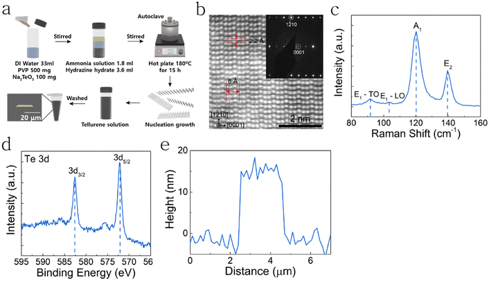 |
| | Fig. 1 Material preparation and characterization of 2D Te. (a) Schematic of the synthesis process for the 2D Te crystal; the scale bar in the optical microscopy image is 20 μm. (b) HAADF image and SAED pattern obtained with the synthesized 2D Te flake. The atomic structure exhibits three-fold symmetry with a helical chain along 〈0001〉. (c) Raman spectra of tellurene. The Raman intensity corresponds to the A1, E1, and E2 modes. (d) XPS spectra of the Te 3d region. (e) Height profile of a 16 nm-thick 2D tellurene flake. | |
The electrical characteristics of the h-BN/Te device were studied to determine its feasibility as an artificial synapse. A flexible h-BN/Te top-gate device was fabricated on a polyethylene terephthalate (PET) substrate, as shown in Fig. 2(a). Considering the variation in electrical characteristics based on the crystal orientation of 2D Te, a device channel with a length of 3 μm and a 3 μm width between the source and drain was constructed along the [0001] direction through the conventional photolithography technique (Fig. S4, ESI†).40 A charge-trapping layer must be formed to facilitate charge-trapping or de-trapping.49 We made the channel conductivity adjustable by applying O2 plasma treatment to h-BN (Fig. S5, ESI†). The Raman spectra and Raman mapping images of the h-BN transferred onto Te demonstrate that h-BN uniformly encapsulated the entire Te nanoflake, indicating the formation of a charge-trapping layer in all regions of the 2D Te flake (Fig. S6, ESI†). Fig. 2(b) illustrates the electronic transfer characteristics of the h-BN/Te device at VDS = 0.01 V. The transfer curve exhibits a threshold voltage (VTH) of 7.23 V with p-type conductivity. Furthermore, the h-BN/Te field-effect transistor (FET) showed a field-effect mobility of 56.2 cm2 V−1 s−1, along with a subthreshold swing of 2.06 V per decade. The current on/off ratio within a 20 V bias is 3.6 × 10². These results demonstrate that the h-BN/Te top-gate device was effectively fabricated. The output characteristics of the FET exhibit distinct symmetric and linear behaviors. This indicates the successful formation of Ohmic contacts within the source and drain electrodes, as shown in Fig. 2(c). Notably, anticlockwise hysteresis characteristics were observed in Fig. 2(d), indicating that the operating mechanism is charge-trapping or de-trapping.50 The hysteresis window was broadened with the increase in ΔVGS. These gate-controlled electronic transfer characteristics verify the existence of programmable multilevel conductance states in the h-BN/Te FET. We exposed the h-BN/Te device to ambient conditions for 3 weeks to demonstrate its environmental stability. The transfer characteristics of the h-BN/Te device exhibited negligible hysteresis and current level changes for 3 weeks under ambient conditions, as shown in Fig. 2(e). In addition, a slight variation in VTH was observed in the write and erase operation modes over 1000 cycles, indicating excellent reliability (Fig. 2(f)). These results demonstrate that the h-BN/Te top-gate transistor is suitable for wearable synaptic devices.
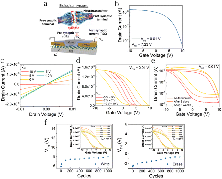 |
| | Fig. 2 Electrical characteristics of a flexible h-BN/Te top-gate transistor. (a) Schematic of the h-BN/Te synaptic device. (b) Transfer curves and (c) output curves of the h-BN/Te FET. (d) Hysteresis curves in transfer characteristics under VDS = 0.01 V. (e) Hysteresis curves of the h-BN/Te device over time after fabrication. (f) Endurance characteristics of the h-BN/Te transistor. | |
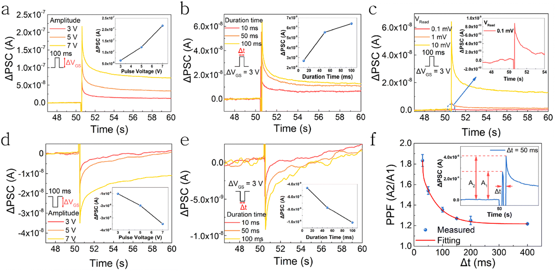
Biological synapses are microscopic gaps between the pre- and postsynaptic terminals.51,52 A presynaptic neuron generates an action potential when an input spike exceeding the threshold is applied. Subsequently, neurotransmitters are released from the presynaptic terminals and engage with receptors on the dendrites of the postsynaptic terminals. Owing to this interaction, the synapses shape the biological memory and behaviors of human beings.53 We reconfigured the gate and drain electrodes of the 2D Te FET as the presynaptic and postsynaptic neurons, respectively, to replicate these interactions. To confirm the short-term synaptic plasticity of the wearable artificial synaptic transistors, we explored their excitatory and inhibitory postsynaptic current (EPSC and IPSC) characteristics, as shown in Fig. 3(a)–(f) where different pulse amplitudes and time durations were applied to the gate-generated PSCs in the artificial synapses.
 |
| | Fig. 3 The gate terminal, which is a presynaptic terminal, was modified to mimic biological synaptic behavior. EPSC characteristics under (a) different amplitudes of 3, 5, and 7 V (read voltage: 0.01 V, time duration: 100 ms) and (b) different time durations of 10, 50, and 100 ms (read voltage: 0.01 V, amplitude: 3 V); inset: EPSC change curves under different pulses. (c) EPSC curve under different read voltages of 0.1, 1, and 10 mV (amplitude: 3 V, time duration: 100 ms); inset: enlarged EPSC curve with a read voltage of 0.1 mV. IPSC characteristics under (d) different amplitudes of 3, 5, and 7 V (read voltage: 0.01 V, time duration: 100 ms) and (e) different time durations of 10, 50, and 100 ms (read voltage: 0.01 V, amplitude: 3 V); inset: IPSC change curves under different pulses. (f) PPF index with different time intervals with a VGS of 2 V for 50 ms (read voltage: 0.01 V); inset: EPSC curve triggered by a pair of presynaptic spikes with an interval. | |
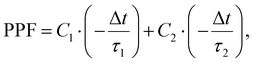
Fig. 3(a) illustrates the EPSC characteristics of the flexible 2D Te artificial synaptic transistors as a function of different gate voltages (VGS) under a constant drain read voltage of 0.01 V and pulse width of 100 ms. The increase in the gate voltage amplitudes from 3 to 7 V increased the ΔPSC from 65 to 217 nA. Furthermore, the increase in the spiking pulse width increased the EPSCs at a fixed pulse magnitude of 3 V and read voltage of 0.01 V, as shown in Fig. 3(b). Additionally, an increased VDS resulted in enhanced EPSCs, as shown in Fig. 3(c). Fig. 3(d) and (e) show the IPSC contours for an identical platform. They exhibited a trend similar to that of the EPSC characteristics, except for the opposite negative pulse polarity. These results demonstrate that the electrical modulations of the pre- and postsynaptic terminals regulate the short-term synaptic plasticity of the flexible 2D Te artificial synaptic transistors, indicating excellent replication of biological networks. We analyzed the paired-pulse facilitation (PPF) of the flexible 2D Te artificial templates to obtain a deeper insight into their short-term synaptic plasticity characteristics, as shown in Fig. 3(f). PPF is a form of short-term synaptic plasticity triggered by presynaptic spikes with pulse interval times (Δt) and defined by A2 over A1.54,55 Here, A1 and A2 represent the peaks of the first and second PSC spikes, respectively, as shown in the inset of Fig. 3(f). The strength of PPF in the artificial platform steadily weakened with the increase in Δt. The short-term plasticity strength of the flexible 2D Te artificial synaptic transistors clearly belongs to the following double exponential decay equation:56
| |  | (1) |
where Δ
t represents the time interval between
A1 and
A2.
C1 and
C2 represent the initial facilitation magnitudes of the fast and slow phases, respectively.
τ1 and
τ2 represent the relaxation times of the rapid and slow phases, respectively, which were estimated to be 1.83 and 55.5 ms, respectively. These values concur well with the spiking activity dimension of the typical biological nerve network. All the results effectively demonstrate that the flexible artificial 2D Te transistor exhibits the short-term plasticity (STP) characteristics of a biological synaptic system. Additionally, this demonstrates that the artificial 2D Te synaptic architectures show excellent neuromorphic computational capabilities. Furthermore, to assess its potential as an artificial synaptic device with edge-computing capabilities, we calculated the power consumption using the following equation:
57| | | Econsumption = Vread × Ipeak × tpulse, | (2) |
where
Vread,
Ipeak, and
tpulse represent the drain voltage, EPSC peak current, and pulse width, respectively. We obtained an extremely low power consumption of 9 fJ in a flexible 2D Te artificial synaptic transistor under a single pulse with a
VDS of 0.1 mV, an amplitude of 3 V, and a duration of 100 ms. We attribute the remarkable energy efficiency, achieved without the need for intricate fabrication processes, to the physical characteristics of 2D Te with a narrow band gap and high carrier density. This demonstrates that the power consumption characteristics of the flexible 2D Te artificial devices were comparable or superior to those of other 2D synaptic transistors reported in previous studies, presenting an energy-efficient wearable neuromorphic edge architecture.
34,58–61 Furthermore, it is proved that the flexible 2D Te synaptic transistor can properly emulate artificial synaptic systems considering synapses in the human brain consume approximately 10 fJ per pulse.
19
We analyzed the long-term potentiation (LTP) and depression (LTD) characteristics of flexible 2D Te artificial synaptic transistors under various electrical presynaptic triggers to elucidate their long-term synaptic plasticity and reconfigurable capacity. Fig. 4 depicts five different LTP/LTD patterns of the artificial synaptic transistor under 100 consecutive electrical potentiation and depression-spiking modulations. One hundred constant single pulses with an amplitude of 4 V, a pulse width of 50 ms, and an impulse interval time of 70 ms were applied for both potentiation and depression, as shown in Fig. 4(a). They demonstrate robust write and erase operations for learning and memory behaviors in the flexible artificial synapses. This presented an abrupt increase in the conductance for both the LTP and LTD. The corresponding potentiation impulse and decreased gate spiking magnitude from −4 to −1 V in the depression array resulted in a moderately decreased slope in the LTD, as shown in Fig. 4(b). Fig. 4(c) illustrates the ascending stepwise gate impulse magnitude arrangement from 1 to 4 V for the potentiation and the depression at a fixed negative spiking progression of −1 V. A more moderate increment in conductance in the LTP sequence was observed when compared to that in Fig. 4(b). A stepwise presynaptic electrical spiking array from 1 to 4 V in both the potentiation and depression arrangements improved the symmetry of the LTP/LTD curve, as shown in Fig. 4(d). A reduced gate spiking magnitude of −0.1 V with a spiking step of 40 mV at the starting point of the depression arrangement and the corresponding potentiation bias from Fig. 4(e) shaped a more balanced erasing feature in the depression stage. The gate tunability of the learning feature governs the figure-of-merit of the artificial synaptic devices, such as multilevel states, the dynamic range, symmetry, and linearity.62 The high multilevel states improve the training capability and robustness of the device. The dynamic range, which is the ratio between the maximum conductance (Gmax) and minimum conductance (Gmin), is crucial in terms of the power consumption and mapping capability.63 The symmetry and linearity of the LTP/LTD curve can improve the recognition accuracy of the artificial neural network system. The linearity and symmetry of the LTD/LTD for the flexible 2D Te artificial synaptic transistor were estimated as follows:64
| | | Gp = B(1 − e−P/Ap) + Gmin, | (3) |
| | | Gd = −B(1 − e(P−Pmax)/Ad) + Gmin, | (4) |
| |  | (5) |
| |  | (6) |
where
GP and
GD represent the conductances of long-term potentiation and depression, respectively;
P and
Pmax represent the number of pulses and maximum number of pulses, respectively;
Ap and
Ad represent the non-linearities (NL) for potentiation and depression, respectively; and
B denotes a fitting constant. The wearable 2D Te synaptic transistor exhibited good linearity, and the dynamic ranges (
Gmax/
Gmin) were evaluated as 1.08, 1.06, 1.05, 1.06, and 1.05 for
Fig. 4(a)–(e). The asymmetry ratio (AR) values were calculated as 0.65, 0.59, 0.27, 0.2, and 0.2, respectively. The values of effective conductance state, which is the entire conductance difference (Δ
G =
Gmax −
Gmin) above a threshold of 0.5%, were estimated to be 42, 40, 85, 93, and 93, respectively (Table S1, ESI
†). The variations of the LTP/LTD curve through gate tunability demonstrated that the wearable 2D Te synaptic transistor exhibited outstanding long-term plasticity and reconfigurability for the learning behaviors of the neuromorphic-edge-computing platform. Additionally, it is remarkable that the synaptic performance of the 2D Te flexible synaptic device is comparable or superior to others reported previously (Table S2, ESI
†).
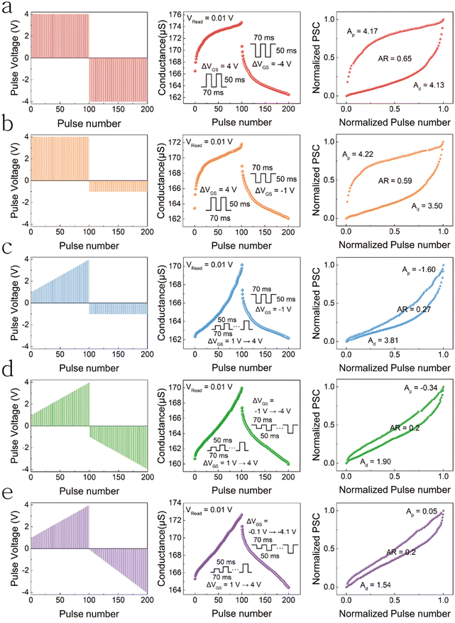 |
| | Fig. 4 Controllability of LTP/LTD characteristics for different pulse patterns under a read voltage of 0.01 V (base: 3 V). (a) LTP/LTD characteristic curves under potentiation pulses with a VGS of 4 V and depression pulses with a VGS of −4 V. (b) LTP/LTD characteristic curves under potentiation pulses with a VGS of 4 V and depression pulses with a VGS of −1 V. (c) LTP/LTD characteristic curves under potentiation pulses with a gradual increase in VGS from 1 to 4 V (in steps of 30 mV) and depression pulses with a VGS of −1 V. (d) LTP/LTD characteristic curves under potentiation pulses with a gradual increase in VGS from 1 to 4 V (30 mV step) and depression pulses with a gradual decrease in VGS from −1 to −4 V (30 mV step). (e) LTP/LTD characteristic curves under potentiation pulses with a gradual increase in VGS from 1 to 4 V (30 mV step) and depression pulses with a gradual decrease in VGS from −0.1 to −4 V (40 mV step). | |
Electrical stability under mechanical modulation is highly promising for flexible electronics such as wearable edge computing, soft robotics, and neuroprosthetics. To elucidate the mechanical stability and flexibility of the flexible 2D Te artificial template, we analyzed the LTP and LTD stabilities of the 2D Te artificial synaptic transistors under different bending strains, as shown in Fig. 5. Fig. 5(a) shows a photograph of a flexible 2D Te FET mounted on a PET substrate with a bending force. Fig. 5(b) shows the endurance characteristics in the flat, convex, and concave bending states. The bending strain was calculated as ε = t/ρ, where t denotes the thickness of the substrate and ρ denotes the bending radius (Fig. S7, ESI†).65 The trajectory of the LTP/LTD sequence was achieved by applying 2000 sequential electrical pulses for VGS, from 1 to 4 V (with a ΔV of 30 mV) for potentiation and from 0.1 to 4.1 V (with a ΔV of 40 mV) for depression, along with a VDS of 0.01 V. It can be observed that the flexible 2D Te artificial synaptic transistors exhibit excellent mechanical stability and reconfigurability via gate tunability, regardless of the bending status on the devices, demonstrating their potential for future applications (Table S3, ESI†). Notably, artificial synapses with convex and concave bending exhibited 100 and 79 effective states, respectively. The effective state in the flat state was 93. Furthermore, the flexible artificial synaptic transistor with concave bending exhibited a much lower conductance level over the entire measurement range when compared to other synaptic devices. These characteristics are attributed to the generation of the piezoelectric field and variation in the surface contact area of O2 or H2O molecules. The piezoelectric effect occurs when strain is applied to the lattice of Te, which has a trigonal crystal lattice structure. This strain causes a deformation that eliminates the inversion symmetry of the Te crystal lattice, leading to the emergence of ion charge polarization.66 In this case, according to the convenience of piezoelectric theory, the piezoelectric polarization charges are regarded as surface charges on the bulk piezoelectric material.67 When a negative piezoelectric polarization charge is induced in a p-FET, it causes the majority carriers, which are holes, to accumulate at the interface, resulting in a reduction of the Schottky barrier height (SBH). Conversely, the induction of a positive piezoelectric polarization charge repels holes from the interface, leading to an increase in the SBH.68 In convex bending, a negative piezoelectric polarization charge is induced on the source–Te interface and a positive charge on the drain–Te interface. This leads to a decrease in the SBH at the source side and an increase at the drain side, facilitating the flow of more holes and improving FET conductance. Conversely, in concave bending, a positive piezoelectric polarization charge is induced on the source–Te interface and a negative charge on the drain–Te interface. This results in an increased SBH at the source side and a decreased SBH at the drain side interface, causing a reduction in hole flow compared to the flat state and resulting in reduced performance. Furthermore, the crystallographic orientation of the Te lattice can govern the direction of the piezoelectric polarization charge.69,70 This nature is currently under study. Another reason for conductance changes due to bending is changes in the surface contact area of O2 or H2O molecules, which can change the amount of charge carrier trapping/detrapping, leading to changes in conductance values.71,72 Based on the results of the 10 cycles LTP/LTD curve, we implemented a backpropagation algorithm to confirm the learning and recognition characteristics of artificial neural network (ANN) simulation. The network structure is a simple model, as shown in Fig. 5(c). It is a two-layer perceptron neural network with 784 input neurons, with 300 neurons in the hidden layers and 10 neurons in the output layers. We used handwritten digits of 28 × 28 pixels based on the MNIST dataset. The pattern recognition accuracy was indicated by 40 training epochs, and Fig. 5(d) shows the simulation results of the flexible 2D Te synaptic transistor with different strains. In the case of convex bending, the artificial 2D Te synaptic transistor immediately achieved an accuracy of 90% in the first training epoch and subsequently achieved a high recognition rate of 94%. The flexible 2D Te artificial platform with concave bending exhibited an accuracy of approximately 88%, which is slightly lower than the accuracy of 93% in the flat state but still considered a comparable or superior level compared to those of previous studies.45,73 In conclusion, the flexible 2D Te artificial synaptic transistor presents considerable potential in wearable neuromorphic edge computing devices requiring outstanding mechanical stability.
 |
| | Fig. 5 (a) Photograph of the 2D Te synaptic transistor on a PET substrate. (b) Endurance characteristics of wearable devices for 10 cycles operating under flat, convex, and concave bending strain. (c) Schematic of a two-layer perceptron neural network on the MNIST 28 × 28 pixel handwritten digit data set. (d) Simulated recognition accuracy based on MNIST dataset comparison for flat, convex bending, and concave bending conditions. | |
Conclusions
In this study, we fabricated flexible artificial synaptic transistors using 2D Te on a flexible substrate for bio-inspired wearable neuromorphic edge computing. The dielectric layer, h-BN, underwent O2 plasma treatment, forming a charge-trapping/de-trapping layer, which enabled the adjustment of the channel conductivity. The 2D Te synaptic transistor demonstrated an extremely low power consumption of 9 fJ and exhibited excellent synaptic plasticity under various pulse conditions. Furthermore, it exhibited high linearity and symmetry in the LTP/LTD characteristics, resulting in an impressive accuracy of 93% in recognizing MNIST patterns. Additionally, it was observed to be a flexible synaptic transistor with outstanding gate tunability and endurance characteristics, even under a 2% curvature in both the concave and convex states. This study presents a promising platform for flexible synaptic transistors by employing robust 2D Te and contributes significantly to the realization of future wearable neuromorphic edge computing applications.
Author contributions
B. You and J. Yoon designed the experiments, analyzed the data, performed the experiments, interpreted the results, and wrote the manuscript. Y. Kim performed all the experiments. M. Yang analyzed the data. J. Bak and J. Park conducted the experiments. U. Kim supervised the research. M. G. Hahm supervised the study. M. Lee designed the experiments, wrote the manuscript, and supervised the project.
Conflicts of interest
The authors declare no competing financial interests.
Acknowledgements
This work was supported by the National Research Foundation of Korea (NRF) grant funded by the Korean Government (MSIT) (grant no. NRF-2021R1C1C1004794) and INHA UNIVERSITY Research Grant.
References
- U. Paschen, C. Pitt and J. Kietzmann, Bus. Horiz., 2020, 63, 147–155 CrossRef.
- H. Tran-Dang, N. Krommenacker, P. Charpentier and D.-S. Kim, IEEE Internet Things J., 2020, 7, 4711–4736 Search PubMed.
- S. Dai, Y. Zhao, Y. Wang, J. Zhang, L. Fang, S. Jin, Y. Shao and J. Huang, Adv. Funct. Mater., 2019, 29, 1903700 CrossRef CAS.
- M. A. Zidan, J. P. Strachan and W. D. Lu, Nat. Electron., 2018, 1, 22–29 CrossRef.
- S. Liu, Y. Wang, M. Fardad and P. K. Varshney, IEEE Circuits Syst. Mag., 2018, 18, 29–44 Search PubMed.
- G. W. Burr, R. M. Shelby, A. Sebastian, S. Kim, S. Kim, S. Sidler, K. Virwani, M. Ishii, P. Narayanan and A. Fumarola, Adv. Phys.: X, 2017, 2, 89–124 Search PubMed.
- Y. Wang, L. Yin, W. Huang, Y. Li, S. Huang, Y. Zhu, D. Yang and X. Pi, Adv. Intell. Syst., 2021, 3, 2000099 CrossRef.
- B. Sun, T. Guo, G. Zhou, S. Ranjan, Y. Jiao, L. Wei, Y. N. Zhou and Y. A. Wu, Mater. Today Phys., 2021, 18, 100393 CrossRef CAS.
- Z. Lv, Y. Wang, J. Chen, J. Wang, Y. Zhou and S.-T. Han, Chem. Rev., 2020, 120, 3941–4006 CrossRef CAS PubMed.
- X. Zou, S. Xu, X. Chen, L. Yan and Y. Han, Sci. China Inf. Sci., 2021, 64, 160404 CrossRef.
- J. Q. Yang, R. Wang, Y. Ren, J. Y. Mao, Z. P. Wang, Y. Zhou and S. T. Han, Adv. Mater., 2020, 32, 2003610 CrossRef PubMed.
- K. Roy, A. Jaiswal and P. Panda, Nature, 2019, 575, 607–617 CrossRef CAS PubMed.
- J. Tang, F. Yuan, X. Shen, Z. Wang, M. Rao, Y. He, Y. Sun, X. Li, W. Zhang and Y. Li, Adv. Mater., 2019, 31, 1902761 CrossRef CAS PubMed.
- J.-H. Ryu, B. Kim, F. Hussain, C. Mahata, M. Ismail, Y. Kim and S. Kim, Appl. Surf. Sci., 2021, 544, 148796 CrossRef CAS.
- S. Rajasekaran, F. M. Simanjuntak, S. Chandrasekaran, D. Panda, A. Saleem and T.-Y. Tseng, IEEE Electron Device Lett., 2021, 43, 9–12 Search PubMed.
- A. Saleem, D. Kumar, A. Singh, S. Rajasekaran and T. Y. Tseng, Adv. Mater. Technol., 2022, 7, 2101208 CrossRef CAS.
- Y. Lee and T.-W. Lee, Acc. Chem. Res., 2019, 52, 964–974 CrossRef CAS PubMed.
- G. Yushan, Z. Junyao, L. Dapeng, S. Tongrui, W. Jun, L. Li, D. Shilei, Z. Jianhua, Y. Zhenglong and H. Jia, Chin. Chem. Lett., 2023, 108582 Search PubMed.
- H. L. Park, Y. Lee, N. Kim, D. G. Seo, G. T. Go and T.
W. Lee, Adv. Mater., 2020, 32, 1903558 CrossRef CAS.
- M. Aitsam, S. Davies and A. Di Nuovo, IEEE Access, 2022, 10, 122261–122279 Search PubMed.
- D.-G. Seo, Y. Lee, G.-T. Go, M. Pei, S. Jung, Y. H. Jeong, W. Lee, H.-L. Park, S.-W. Kim and H. Yang, Nano Energy, 2019, 65, 104035 CrossRef CAS.
- N. Liu, L. Q. Zhu, P. Feng, C. J. Wan, Y. H. Liu, Y. Shi and Q. Wan, Sci. Rep., 2015, 5, 18082 CrossRef CAS PubMed.
- G. Zhong, M. Zi, C. Ren, Q. Xiao, M. Tang, L. Wei, F. An, S. Xie, J. Wang and X. Zhong, Appl. Phys. Lett., 2020, 117, 092903 CrossRef CAS.
- M. Prezioso, F. Merrikh-Bayat, B. D. Hoskins, G. C. Adam, K. K. Likharev and D. B. Strukov, Nature, 2015, 521, 61–64 CrossRef CAS PubMed.
- S. Yu, Y. Wu, R. Jeyasingh, D. Kuzum and H.-S. P. Wong, IEEE Trans. Electron Devices, 2011, 58, 2729–2737 CAS.
- Y. Wang, Z. Lv, J. Chen, Z. Wang, Y. Zhou, L. Zhou, X. Chen and S. T. Han, Adv. Mater., 2018, 30, 1802883 CrossRef PubMed.
- H.-L. Park and T.-W. Lee, Org. Electron., 2021, 98, 106301 CrossRef CAS.
- Y. van De Burgt, A. Melianas, S. T. Keene, G. Malliaras and A. Salleo, Nat. Electron., 2018, 1, 386–397 CrossRef.
- F. Ma, Y. Zhu, Z. Xu, Y. Liu, X. Zheng, S. Ju, Q. Li, Z. Ni, H. Hu and Y. Chai, Adv. Funct. Mater., 2020, 30, 1908901 CrossRef CAS.
- R. A. John, N. Yantara, S. E. Ng, M. I. B. Patdillah, M. R. Kulkarni, N. F. Jamaludin, J. Basu, N. Ankit, S. G. Mhaisalkar and A. Basu, Adv. Mater., 2021, 33, 2007851 CrossRef CAS.
- X. Gu, M. Zhou, Y. Zhao, Q. Zhang, J. Zhang, Y. Huang and S. Lu, Nano Res., 2023, 1–9 Search PubMed.
- M. Zhou, Y. Zhao, X. Gu, Q. Zhang, J. Zhang, M. Jiang and S. Lu, Photonics Res., 2023, 11, 1667–1677 CrossRef.
- V. K. Sangwan and M. C. Hersam, Nat. Nanotechnol., 2020, 15, 517–528 CrossRef CAS PubMed.
- J. Jiang, J. Guo, X. Wan, Y. Yang, H. Xie, D. Niu, J. Yang, J. He, Y. Gao and Q. Wan, Small, 2017, 13, 1700933 CrossRef PubMed.
- G. Cao, P. Meng, J. Chen, H. Liu, R. Bian, C. Zhu, F. Liu and Z. Liu, Adv. Funct. Mater., 2021, 31, 2005443 CrossRef CAS.
- W. Huh, D. Lee and C. H. Lee, Adv. Mater., 2020, 32, 2002092 CrossRef CAS PubMed.
- B. Radisavljevic, A. Radenovic, J. Brivio, V. Giacometti and A. Kis, Nat. Nanotechnol., 2011, 6, 147–150 CrossRef CAS PubMed.
- G. Eda, G. Fanchini and M. Chhowalla, Nat. Nanotechnol., 2008, 3, 270–274 CrossRef CAS PubMed.
- Q. Sun, D. H. Kim, S. S. Park, N. Y. Lee, Y. Zhang, J. H. Lee, K. Cho and J. H. Cho, Adv. Mater., 2014, 26, 4735–4740 CrossRef CAS PubMed.
- Y. Wang, G. Qiu, R. Wang, S. Huang, Q. Wang, Y. Liu, Y. Du, W. A. Goddard III, M. J. Kim and X. Xu, Nat. Electron., 2018, 1, 228–236 CrossRef.
- L. Tong, X. Huang, P. Wang, L. Ye, M. Peng, L. An, Q. Sun, Y. Zhang, G. Yang and Z. Li, Nat. Commun., 2020, 11, 2308 CrossRef CAS.
- N. R. Glavin, R. Rao, V. Varshney, E. Bianco, A. Apte, A. Roy, E. Ringe and P. M. Ajayan, Adv. Mater., 2020, 32, 1904302 CrossRef CAS.
- D. Wines, J. A. Kropp, G. Chaney, F. Ersan and C. Ataca, Phys. Chem. Chem. Phys., 2020, 22, 6727–6737 RSC.
- C. Shen, Y. Liu, J. Wu, C. Xu, D. Cui, Z. Li, Q. Liu, Y. Li, Y. Wang and X. Cao, ACS Nano, 2019, 14, 303–310 CrossRef.
- J. Yoon, B. You, Y. Kim, J. Bak, M. Yang, J. Park, M. G. Hahm and M. Lee, ACS Appl. Mater. Interfaces, 2023, 15, 18463–18472 CrossRef CAS PubMed.
- D. Wang, A. Yang, T. Lan, C. Fan, J. Pan, Z. Liu, J. Chu, H. Yuan, X. Wang and M. Rong, J. Mater. Chem. A, 2019, 7, 26326–26333 RSC.
- R. Jain, Y. Yuan, Y. Singh, S. Basu, D. Wang, A. Yang, X. Wang, M. Rong, H. J. Lee and D. Frey, Adv. Energy Mater., 2021, 11, 2003248 CrossRef CAS.
-
D. R. Lide, CRC handbook of chemistry and physics, CRC press, 2004 Search PubMed.
- A. J. Arnold, A. Razavieh, J. R. Nasr, D. S. Schulman, C. M. Eichfeld and S. Das, ACS Nano, 2017, 11, 3110–3118 CrossRef CAS PubMed.
- M. Zhang, Z. Fan, X. Jiang, H. Zhu, L. Chen, Y. Xia, J. Yin, X. Liu, Q. Sun and D. W. Zhang, Nanophotonics, 2020, 9, 2475–2486 CrossRef CAS.
- W. C. Yang, Y. C. Lin, S. Inagaki, H. Shimizu, E. Ercan, L. C. Hsu, C. C. Chueh, T. Higashihara and W. C. Chen, Adv. Sci., 2022, 9, 2105190 CrossRef CAS PubMed.
- J. Shi, S. D. Ha, Y. Zhou, F. Schoofs and S. Ramanathan, Nat. Commun., 2013, 4, 2676 CrossRef PubMed.
- T. You, M. Zhao, Z. Fan and C. Ju, Sensors, 2023, 23, 5413 CrossRef CAS PubMed.
- Y. H. Liu, L. Q. Zhu, P. Feng, Y. Shi and Q. Wan, Adv. Mater., 2015, 27, 5599–5604 CrossRef CAS PubMed.
- L. Q. Zhu, C. J. Wan, L. Q. Guo, Y. Shi and Q. Wan, Nat. Commun., 2014, 5, 3158 CrossRef PubMed.
- S. Shin, D. C. Kang, K. Kim, Y. Jeong, J. Kim, S. Lee, J. Y. Kwak, J. Park, G. W. Hwang and K.-S. Lee, Mater. Adv., 2022, 3, 2827–2837 RSC.
- N. Yang, J. Zhang, J.-K. Huang, Y. Liu, J. Shi, Q. Si, J. Yang and S. Li, ACS Appl. Electron. Mater., 2022, 4, 3154–3165 CrossRef CAS.
- C. S. Yang, D. S. Shang, N. Liu, G. Shi, X. Shen, R. C. Yu, Y. Q. Li and Y. Sun, Adv. Mater., 2017, 29, 1700906 CrossRef PubMed.
- J. Yuan, S. E. Liu, A. Shylendra, W. A. Gaviria Rojas, S. Guo, H. Bergeron, S. Li, H.-S. Lee, S. Nasrin and V. K. Sangwan, Nano Lett., 2021, 21, 6432–6440 CrossRef CAS PubMed.
- N. K. Upadhyay, H. Jiang, Z. Wang, S. Asapu, Q. Xia and J. Joshua Yang, Adv. Mater. Technol., 2019, 4, 1800589 CrossRef.
- S. Wang, L. Liu, L. Gan, H. Chen, X. Hou, Y. Ding, S. Ma, D. W. Zhang and P. Zhou, Nat. Commun., 2021, 12, 53 CrossRef CAS PubMed.
- M.-K. Kim and J.-S. Lee, Nano Lett., 2019, 19, 2044–2050 CrossRef CAS PubMed.
- K. C. Kwon, Y. Zhang, L. Wang, W. Yu, X. Wang, I.-H. Park, H. S. Choi, T. Ma, Z. Zhu and B. Tian, ACS Nano, 2020, 14, 7628–7638 CrossRef CAS PubMed.
- C. Wang, Y. Li, Y. Wang, X. Xu, M. Fu, Y. Liu, Z. Lin, H. Ling, P. Gkoupidenis and M. Yi, J. Mater. Chem. C, 2021, 9, 11464–11483 RSC.
-
J. M. Gere and B. J. Goodno, Mechanics of materials, Cengage learning, 2012 Search PubMed.
- K.-A. N. Duerloo, M. T. Ong and E. J. Reed, J. Phys. Chem. Lett., 2012, 3, 2871–2876 CrossRef CAS.
- Y. Zhang, Y. Liu and Z. L. Wang, Adv. Mater., 2011, 23, 3004–3013 CrossRef CAS PubMed.
- W. Wu, L. Wang, Y. Li, F. Zhang, L. Lin, S. Niu, D. Chenet, X. Zhang, Y. Hao and T. F. Heinz, Nature, 2014, 514, 470–474 CrossRef CAS PubMed.
- J. Qi, Y.-W. Lan, A. Z. Stieg, J.-H. Chen, Y.-L. Zhong, L.-J. Li, C.-D. Chen, Y. Zhang and K. L. Wang, Nat. Commun., 2015, 6, 7430 CrossRef CAS PubMed.
- H. Zhu, Y. Wang, J. Xiao, M. Liu, S. Xiong, Z. J. Wong, Z. Ye, Y. Ye, X. Yin and X. Zhang, Nat. Nanotechnol., 2015, 10, 151–155 CrossRef CAS PubMed.
- Y. Shimazu, M. Tashiro, S. Sonobe and M. Takahashi, Sci. Rep., 2016, 6, 30084 CrossRef CAS PubMed.
- S. Tongay, J. Zhou, C. Ataca, J. Liu, J. S. Kang, T. S. Matthews, L. You, J. Li, J. C. Grossman and J. Wu, Nano Lett., 2013, 13, 2831–2836 CrossRef CAS PubMed.
- C. Zheng, Y. Liao, J. Wang, Y. Zhou and S.-T. Han, ACS Appl. Mater. Interfaces, 2022, 14, 57102–57112 CrossRef CAS PubMed.
Footnotes |
| † Electronic supplementary information (ESI) available: Schematics of solvent-assisted thinning and drop casting processes, OM and Raman mapping images of 2D Te, surface potential and work function of 2D Te on p-type Si, schematics and OM images of the fabrication method for the flexible 2D Te transistor, data of the comparison before and after O2 plasma treatment on h-BN, schematics of the concave and convex bending models, table summarizing the gate tunability performance of the 2D Te synaptic transistor, performance comparison of previously reported 2D material-based synaptic devices, and performance summary table of convex and concave bending of a 2D tellurium flexible FET (PDF). See DOI: https://doi.org/10.1039/d4tc00530a |
| ‡ These authors contributed equally to this paper. |
|
| This journal is © The Royal Society of Chemistry 2024 |
Click here to see how this site uses Cookies. View our privacy policy here. 
 Open Access Article
 This Open Access Article is licensed under a
  *a
*a