
 Open Access Article
 This Open Access Article is licensed under a
 Creative Commons Attribution 3.0 Unported Licence
Tuning the electrical conductance of oligo(phenylene-ethynylene) derivatives-PbS quantum-dot bilayers†
Ali
Ismael‡
 *ab,
Xintai
Wang‡
*cde,
Alaa
Al-Jobory‡
af,
Shanglong
Ning‡
d,
Turki
Alotaibi‡
ag,
Bashayr
Alanazi
ah,
Hanan
Althobaiti
ai,
Junsheng
Wang
c,
Naixu
Wei
e,
Christopher J. B.
Ford
*d and
Colin J.
Lambert
*a
*ab,
Xintai
Wang‡
*cde,
Alaa
Al-Jobory‡
af,
Shanglong
Ning‡
d,
Turki
Alotaibi‡
ag,
Bashayr
Alanazi
ah,
Hanan
Althobaiti
ai,
Junsheng
Wang
c,
Naixu
Wei
e,
Christopher J. B.
Ford
*d and
Colin J.
Lambert
*a
aPhysics Department, Lancaster University, Lancaster, LA1 4YB, UK. E-mail: k.ismael@lancaster.ac.uk; c.lambert@lancaster.ac.uk
bDepartment of Physics, College of Education for Pure Science, Tikrit University, Tikrit, Iraq
cSchool of Information Science and Technology, Dalian Maritime University, Dalian, China. E-mail: xintaiwang@dlmu.edu.cn
dDepartment of Physics, Cavendish Laboratory, University of Cambridge, Cambridge, CB3 0HE, UK. E-mail: cbjf@cam.ac.uk
eZhejiang Mashang GM2D Technology Research Institute, Cangnan, Wenzhou, Zhejiang, China
fDepartment of Physics, College of Science, University of Anbar, Anbar, Iraq
gDepartment of Physics, College of Science, Jouf University, Skaka, Kingdom of Saudi Arabia
hDepartment of Physics, College of Science, Northern Border University, Arar, Kingdom of Saudi Arabia
iDepartment of Physics, College of Science, Taif-University, Taif, Kingdom of Saudi Arabia
First published on 7th August 2024
Abstract
Transcribing quantum effects from lower to higher dimensions is a complex yet intriguing area of research. Coulomb blockade (CB), a fundamental quantum phenomenon, is commonly observed in low-dimensional materials like quantum dots (QDs) at extremely low temperatures. This behavior shows promise for the development of high-performance memory and thermoelectric devices. However, when transitioning to larger dimensions, such as arrays at room temperature, the CB effect is hindered by thermal fluctuations and structural inconsistencies. This study presents a thorough examination of electron transport through PbS QDs using a blend of experimental and theoretical methods. By creating a sizable parallel array of QDs immobilized on self-assembled monolayers (SAMs) and employing single-layer graphene (SLG) as the top electrode, we were able to maintain the CB effect at room temperature on a device scale. Additionally, a device with a top gate structure was designed to precisely regulate the energetic position of quantum states in relation to the Fermi level of the electrode. By utilizing ultra-small QDs (typically 2 nm in size), we successfully sustained the CB effect at room temperature. To investigate the impact of structural uncertainties, we combined density-functional theory and quantum transport theory to comprehensively analyze the quantum transport properties of QDs bound with SAMs across various facets. This enabled us to establish a correlation between these structural variations and the experimental data distribution.
Molecular-scale logic gates, sensors, memory devices and thermoelectric energy harvesters1–11 have the potential to significantly reduce power consumption and enhance sensitivity. These advancements could be achieved as single-molecule devices (which are not easily mass-produced) or molecular thin films composed of self-assembled molecular layers (SAMs).12–21 To realise the latter, strategies for assembling multilayers of organic molecules have been explored.22–28 Many of these have demonstrated that the electron transport properties of molecular wires can be manipulated by chemically altering their anchor groups used to couple with the electrodes, thereby adjusting the alignment of molecular orbitals.29–34 Most break-junction-based studies of molecular-scale transport use gold electrodes. Here, to realise larger-area contacts, we develop alternative contacting strategies, either using graphene as a conductive material,21,35,36 and/or a conductive layer of quantum dots. We demonstrate the possibility of combining a layer of PbS quantum dots with graphene to form a top contact on a SAM. In particular, we are interested in the question of how the electrical conductance of such heterostructures depends on the structure of the quantum-dot surface, since such features are known to affect the binding of ligands to isolated quantum dots.37–39
In this work, a series of oligo(arylene ethynylene) (OAE) molecules was designed to compare different molecule–quantum-dot interfaces, using graphene and gold as top and bottom electrodes, respectively. Molecules 1–3 (Fig. 1(a)), were designed33 to provide Au–S–SAM-X + PbS–graphene architectures (Fig. 1(b)), where X = benzene (1), para-pyridine (2) and para-(acetylthio)benzene (3). Molecule 1 has no dedicated second anchor group, molecule 2 has a symmetrical design commonly employed in single-molecule studies and molecule 3 enables investigation of the role of a terminal pyridine unit in the electronic behaviour of molecular junctions. As shown in Fig. 1(c) and Fig. S2, S17 (ESI†), each PbS quantum dot has an octahedral shape (i.e., a polyhedron with 14 faces). Confirmation of the octahedral geometry is provided by our DFT simulations, which show that it corresponds to a minimum energy configuration. Due to the small size of the QDs, our TEM and AFM techniques lack the necessary resolution to fully elucidate the detailed structure of our PbS QDs. Nonetheless, existing publications have demonstrated that QDs synthesized using the approach outlined in this study exhibit a 14-face structure.40,41
 | ||
| Fig. 1 (a) Chemical structures of studied molecules 1–3, plus a PbS quantum dot. (b) Typical schematic of a fabricated junction. (c) 14 possible contact faces of the PbS particle: 6 squares (sq. 1–6), and 8 hexagons (hex. 1–8), grey and yellow colors represent Pb and S atoms, respectively. | ||
Results and discussion
We will first describe modelling results, and then compare them with our experimental measurements on similar structures. The transport properties of the three types of junctions were modelled using a combination of density-functional theory (DFT) and quantum transport theory. To understand their possible binding configurations, the three molecular-PbS heterostructures were assembled by combining the two components and then allowing the system to become fully relaxed, as illustrated in Fig. S3 (ESI†). To calculate the electrical transport through molecule–quantum-dot bilayers 1–3, we modelled the bilayer junctions as shown in Fig. S18–S20 and S23–S24 (ESI†) (for more details see Section 1.6 in the ESI†).As a first step towards understanding their electronic properties, the frontier orbitals of the quantum dot were computed. As shown in Fig. S4 (ESI†), the highest occupied molecular orbitals (HOMO) and lowest unoccupied orbitals (LUMO), as well as the (HOMO−1) and (LUMO+1) of the PbS quantum dots have more weight on certain faces. To investigate the possible structures of the multilayers, the quantum dot was attached to the graphene sheet, as shown in Fig. S5 (ESI†), and then the quantum dot with the graphene sheet plus the three molecules (Fig. S6–S8, ESI†) were constructed and fully relaxed.
Comparison between the frontier molecular-orbital plots of Fig. S6–S8 (ESI†) shows that there is no weight on the contact area between molecule 1 and PbS quantum dot (more specifically on 1, for the four plots), whereas there is significant weight on contact areas of molecules 2 and 3. This suggests that there is a relatively weak bond between the PbS and 1, compared with 2 and 3, due to the fact that the phenyl ring is an ineffective anchor group compared to pyridyl and thiol. To confirm this suggestion, we first investigated the binding energies and optimum distances (d) of the bond between the quantum dot and Gr sheet for both S and Pb atoms (Fig. S9, ESI†). Next, we investigated binding energies and optimum distances of molecule 1 to PbS through two different sites (i.e., Pb and S atoms), and similarly, for 2 and 3, as shown in Fig. S10–S15 (ESI†). These results are summarized in Table S1 (ESI†), which clearly demonstrates that molecule 1 does not bind to either S or Pb atoms of the PbS quantum dot, because the binding energies are 10–100 times lower than their corresponding values for molecules 2 and 3. For example, the thiol (molecule 2) and pyridyl (molecule 3) anchors bind 10 times more strongly than the phenyl ring (molecule 1), through S atoms of the quantum dot and 100 times more strongly to Pb atoms. It should also be noted that the molecules bind much more strongly to Pb atoms in the PbS quantum dot than to its S atoms. For more details, see the binding-energy section in the ESI.†
The 14 faces of the PbS quantum-dot truncated octahedron consist of 8 regular hexagons and 6 squares. There are two types of square faces: pristine Pb faces with purely Pb atoms (sq. 1–4), and square faces with a mixture of S and Pb atoms (sq. 5 and 6). On the other hand, all hexagons are identical and contain a mixture of S and Pb atoms (hex. 1–8), as illustrated in Fig. 1(a) and (c). Fig. 1(c) illustrates the 14 possible contacting faces. In Fig. S17a, b and Sections 1.5, 1.6 in the ESI,† the 6 square and 8 hexagonal faces are illustrated by 8 grey and yellow lines. The yellow and grey circles represent S and Pb atoms respectively. We refer to the combination of a molecule with PbS as a (molecule-PbS) bilayer, numbered in the same way as the molecules. Since binding-energy simulations suggest that 1 does not bind to PbS quantum dots, we expect, and later show in our experiments, that the PbS particles will be washed out from the Au-1-SLG junctions, as sketched in Fig. 2(a). The binding-energy simulations also suggest that the PbS quantum dot could bind by either to surface Pb or S atoms, and that the Pb binds more strongly. Taking into account these possibilities, we computed the electron transmission coefficients of 14 junctions for both bilayers 2 and 3![[thin space (1/6-em)]](https://www.rsc.org/images/entities/char_2009.gif) :6 with molecular contacts to square faces (sq. 1–6 as shown in Fig. S19b and S23b, ESI†) and 8 with contacts to hexagonal faces (hex. 1–8 as shown in Fig. S20b and S24b, ESI†), for bilayer 2. For more details, see section 1.6 in the ESI.† Fig. S21 (ESI†) shows the transmission coefficients of bilayer 2, sandwiched between Au and SLG. The 4 grey and 2 black curves correspond to the cases when molecule 2 attaches to 4 pristine Pb and 2 mixed (Pb and S) faces of the PbS quantum dot through square faces, as illustrated in Fig. S19b (ESI†). As expected, the 4 pristine Pb faces yield only small differences in the conductance, as shown by the grey curves. Also, for the mixed square faces, the transmission coefficients are slightly higher than those of pristine Pb faces.
:6 with molecular contacts to square faces (sq. 1–6 as shown in Fig. S19b and S23b, ESI†) and 8 with contacts to hexagonal faces (hex. 1–8 as shown in Fig. S20b and S24b, ESI†), for bilayer 2. For more details, see section 1.6 in the ESI.† Fig. S21 (ESI†) shows the transmission coefficients of bilayer 2, sandwiched between Au and SLG. The 4 grey and 2 black curves correspond to the cases when molecule 2 attaches to 4 pristine Pb and 2 mixed (Pb and S) faces of the PbS quantum dot through square faces, as illustrated in Fig. S19b (ESI†). As expected, the 4 pristine Pb faces yield only small differences in the conductance, as shown by the grey curves. Also, for the mixed square faces, the transmission coefficients are slightly higher than those of pristine Pb faces.
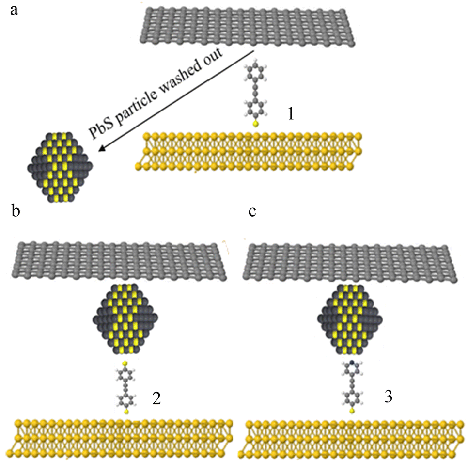 | ||
| Fig. 2 Schematic illustration of the Au-1-3-SLG junctions. Top contact is SLG and the bottom contact is Au. (a) Au-1-SLG junction, the PbS quantum dot is washed away due to the very weak binding between the phenyl ring and PbS. (b) Au-2 + PbS-SLG junction, where the bilayer involves molecules 2 and PbS quantum dots. (c) Au-3 + PbS-SLG junction, where the bilayer involves molecules 3 and PbS quantum dots. | ||
We now consider the case when molecule 2 attaches to 8 different hexagonal faces of the PbS quantum dot, as shown in Fig. S20b (ESI). Since the 8 hexagon faces are a mixture of Pb and S atoms, we computed transmission curves when the studied molecules are contacted to 4 possible S and 4 possible Pb atoms. Fig. S22 (ESI†) shows that contacting to the 8 hexagons yields a smaller variability in the conductances compared to the squares (Fig. S21, ESI†). Fig. S22 (ESI†) also suggests that there are two distinct conductance groups, indicated by orange and grey curves. The two distinct groups are associated with the S and Pb attachment sites. It should be noted that S sites yield slightly higher conductance than Pb sites. A similar trend is obtained for bilayer 3 (see Fig. S23 and S24, ESI†). However, the conductance variability associated with the hexagonal faces is larger, as shown in Fig. S25 and S26 (ESI†). (For more detail, see Section 1.6 in the ESI†). To highlight the effect of the quantum dots on the transport, we repeated the above simulations, but without the PbS quantum dot for the same studied junctions as shown in Fig. S27–S29 (ESI†). (For more details, see Section 1.7 in the ESI†).
Fig. 3(a) shows the DFT simulations of the electrical conductance for the three molecular monolayers 1, 2 and 3 (black, blue and green circles, respectively). For bilayers 2 and 3 (1 does not form a bilayer), two markers are used: circles when the molecule attaches to hexagonal faces and squares when the molecule attaches to square faces. Fig. 3(a) clearly shows that the conductance of the molecular monolayers (without PbS particles) is higher than that of bilayers. This is to be expected, because inserting the quantum dot increases the junction thickness and decreases the conductance. Fig. 3(a) also shows that for both bilayers 2 and 3, bilayers formed from molecules attached to square faces (pink and orange squares), yield higher conductances than those attached to hexagonal faces (pink and orange circles). The pristine Pb square faces yield slightly lower conductances than the mixed faces, despite the fact that Pb binds more strongly than S to the thiol and pyridyl anchors (compare pink and orange squares with black squares). We now compare the above DFT theoretical simulations with experimental electrical conductance measurements of self-assembled mono and bilayers of the three OAE molecules, as shown in Fig. 3(b). These scalable Au–SAM–SLG devices were formed using gold as the bottom electrode and graphene as the top electrode. Detailed device fabrication, SAM and QD growth procedures are presented in Section 2 in the ESI,† and the flowchart illustrations in Fig. S30–S33 (ESI†).
 | ||
| Fig. 3 Comparison between experimental and theoretical (DFT) conductances of the studied molecular monolayers (Au-1–3-SLG) (black, blue, green circles, respectively) and molecule/quantum-dot bilayers (Au-1–3 + PbS-SLG) (red, pink, and orange symbols, respectively). (a) DFT simulations of molecular monolayers are single points, whereas bilayers are multiple points as there are 14 contact faces. Colored squares are for pristine Pb square faces while black squares are for mixed Pb/S square faces. Note that the red point is a molecular monolayer as the PbS quantum dot is washed away and G0 = 2e2/h. (b) Experimental conductance measurements of the corresponding SAMs, as labelled at the bottom. | ||
Fig. 4(a) shows the structure of the device. The micro-well chip consists of a gold bottom electrode covered by a 30 nm thick insulating layer (Al2O3), with a chemically etched microwell for SAM growth. The micro-well chip is connected to a gold pad for linking to the external circuit. Each device consists of 20 micro-well chips, covered by CVD graphene and in contact with two common electrodes without any cover (referred to as common 1 and common 2 in Fig. 4(c)). The in-plane conductance of graphene, GGr, is measured by applying a bias between common 1 and common 2. The measured conductance of the micro-well with molecules (or molecule-QDs) is more than two orders of magnitude lower than GGr. It is observed that the measured conductance of microwell chips remains constant, regardless of whether the counter electrode is common 1 or common 2, confirming that the electric result is not dominated by graphene. The detailed statistics of all measured junctions are listed in Table S2 (ESI†).
 | ||
| Fig. 4 (a) A schematic graph of the device measured in this study. (b) an AFM topographic image of the Au–SAM surface. (c) an AFM topographic image of the Au–SAM–QDs surface. (d) a microscopic image of the micro-device utilized in this research. (e) photoluminescence measurement with corresponding QDs size of the QDs employed in this study. | ||
The synthesis and characterization of QDs used in this work was described in ESI.† Both atomic force microscopy (AFM, Fig. S31, ESI†) and photoluminescence (PL, Fig. S32 and S4(e), ESI†) measurement indicate the size of QDs is about 2 ± 0.5 nm. The SAMs and QDs was deposited onto prepared device as described in ESI.† The Au bottom electrode for the device is prepared by thermo-evaporation, resulting in Au atoms forming grains with a size range of tens to hundreds of nanometers and a surface roughness of 1–2 nm. Consequently, the QDs deposition quality on Au substrate cannot be clearly identified. In this work, template stripped gold with a roughness of 0.1 nm is used to characterize the QDs deposition status. Fig. 4(c) shows the AFM image of Au–SAM 2, where the surface roughness is characterized to be 80 ± 20 pm, with no observed defects. This indicates that the molecules form a closely packed monolayer on the Au substrate. After QDs deposition (Fig. 4(b) and Fig. S36, ESI†), a large number of dots that closely pack on the surface are observed. The clear topography difference between Fig. 4(b) and (c) indicates that these dots are QDs. More than 10 random spots were tested on the SAM–QDs sample, and over 98% of the region was closely covered with QDs. By measuring the height difference between the covered and uncovered regions, it is confirmed that the QDs form a monolayer. Large area scans show a uniform surface, indicating that no multilayer QDs have formed. The lateral size of self assembled QDs is estimated by averaging 200 QDs on the surface, resulting in a value of 6.1 ± 1.2 nm. This result aligns with the size of QDs measured in solution phase by PL, which suggest the average diameter for QDs is 2 ± 0.5 nm (Fig. 4(e)), after considering the tip convolution factor and the external oleic acid ‘shell’ (approximately 1 nm) on both sides (see Fig. S36 and S37, ESI†).
The electric measurement results for each junction system in this study are obtained from at least 3 devices prepared in different batches, and each device contains 17 chips. Occasionally, pinholes formed during SAM formation may result in direct contact between gold and graphene, leading to short circuits (SC). Short circuit junctions exhibit a linear IV shape, high differential conductance near 0 bias, and changes in current density when changing the common contact. For IV analysis and averaging, all SC curves are excluded. In the Au–SAMs system, the occurrence probability of short circuits ranges from 38–44%, whereas in the Au–SAMs–QDs system, this probability drops to less than 10% (Table S2, ESI†). This is expected because the additional QDs layer is large enough to cover the defect regions and decrease the probability of short circuits.
Fig. S38 and S39 (ESI†) show IV curves for SLG–SAM1–Au and SLG–SAM1 + QDs–Au. The typical IV curve shape for the conjugated self-assembled monolayer37 is observed in both cases, which confirms that QDs do not grow on SAM1.
Fig. 5(b) and Fig. S40, S41 (ESI†) show IV curves for SLG–SAM2 + QDs–Au and SLG–SAM3 + QDs–Au. In contrast with SLG–SAM1 + QDs–Au, whose IV curve shapes are identical, the IV curves for SLG–SAM2 + QDs–Au and SLG–SAM3 + QDs–Au show large variations within the chip and some of the junctions show strongly suppressed current at low bias (see Fig. S40(e)–(j) and S41(h)–(j), ESI†). The corresponding result was attributed to the Coulomb blockade behavior from quantum dots. The statistics regarding the behavior of junctions in different self-assembled monolayer (SAM) systems, specifically those exhibiting molecule-like behavior and Coulomb blockade-like behavior, are presented in Table S2 (ESI†). It is evident that none of the Au–SAM junctions displayed Coulomb blockade-like behavior. This observation strongly suggests that the Coulomb blockade-like behavior indeed originates from the presence of quantum dots (QDs). Furthermore, the absence of Coulomb blockade-like behavior in Au–SAM1–QDs, along with the similarity in average conductance between Au–SAM1 and Au–SAM1–QDs, further validates our conclusion that QDs are unlikely to form a layer on SAM1.
 | ||
| Fig. 5 Electron tunnelling through a SAM2–QD bilayer or just SAM2, with a voltage VG applied to an ionic-liquid gate. (a)–(c) I–VSD–VG plot for SAM2–QDs, and corresponding IV and dI/dV curve in the ‘on’ and ‘off’ states. (d)–(f) The same as (a)–(c) but for SAM2 without QDs. (g) On/off ratio for SAM2 and SAM2–QDs at different VSD, taken from (b) and (e), scaled by the gate-voltage spacing between them. (h) Tunnel current near zero VSD (50 mV) as a function of VG, showing Coulomb-blockade peaks. | ||
It is important to note that, for Au–SAM2–QDs and Au–SAM3–QDs, approximately half of the surviving junctions exhibited Coulomb blockade behavior, while the others displayed molecule-like behavior. Although it can be argued that defects in the QDs layer resulting in direct contact between graphene and SAMs may be the origin of the observed molecule-like behavior, the large-scale atomic force microscopy (AFM) scan depicted in Fig. S36(c) (ESI†) suggests that defects were not likely to form in the QDs layer. Additionally, the rigid nature of graphene further reduces the probability of direct contact between graphene and SAMs. Our proposed explanation is that the QDs within the layer exhibit variations in size, binding geometry, and density of state distribution. These variations can lead to the merging of discrete QD levels and suppression of the Coulomb blockade behavior. The presence of a large standard deviation in junction conductance further supports this conclusion. While factors such as roughness of the bottom electrode also contribute to the variation in conductance, the more than 5-fold increase in standard deviation for Au/SAM/QDs compared to their Au/SAM counterparts indicates that QDs is the reason of this extensive data distribution.
Coulomb-blockade behavior is expected to be observable if the capacitance C between the surrounding electrodes/other QDs and a particular QD (of diameter ∼2 nm) gives a charging energy (e2/C) significantly higher than the thermal energy kBT of the system at room temperature T, so that current can only flow once the bias brings the chemical potential of a lead above the electrochemical potential of the dot (which takes into account the charging energy, and the effective gate voltage resulting from the leads and any other background charge).
The Coulomb blockade effect observed in quantum dots (QDs) junctions is widely acknowledged and has been mainly studied in the context of a single QD integrated into a nano-gap. Some reports have demonstrated that even when scaling up the system to large arrays of QDs, the Coulomb blockade behavior persists. However, these studies were conducted at cryogenic temperatures, which are not feasible for practical device applications. In the junction of this study, we focused on a junction where the bottom self-assembled monolayer (SAM) layer and the oleic acid protection layer surrounding the QDs functioned as tunnelling barriers, enabling single-electron transport. We employed ultra-small QDs with a diameter of approximately 2 nm to construct the QDs layer, while the surrounded oleic acid “fur” can isolate them from their neighboring counterparts. The reduced size of these QDs offers a significant advantage, as their charging energy (e2/C) becomes substantially larger than the thermal energy kBT at room temperature. Furthermore, the connections between the QDs and the oleic acid barrier, as well as between the oleic acid barrier and graphene, exhibit weak coupling. This weak coupling plays a critical role in maintaining the integrity of the electron occupancy states within the QD, even at elevated temperatures. By considering these two crucial factors, we successfully observed the Coulomb blockade effect at room temperature.
An inherent advantage of the Coulomb-blockade behavior is its strong sensitivity to changes in the Fermi level. This characteristic makes it highly suitable for high-efficiency devices such as transistors, memories, and sensors. In our study, we manipulated the Fermi level of the graphene electrode by introducing a drop of ionic liquid (DEME-TFSI) onto its surface. Due to the thinness of single-layer graphene (SLG) and its low carrier density, the electric field generated by the gate voltage applied to the ionic liquid can partially penetrate through the graphene layer. Consequently, it alters the energy levels and electrochemical potential of materials beneath graphene relative to the Fermi level in the electrodes. However, a drawback of this gate/graphene/material-based FET structure is that the presence of graphene screens out a portion of the gate voltage (known as the lever-arm effect), resulting in a small energy shift of the Fermi level with respect to the material orbitals even when a large gate voltage is applied, and large gate voltage leads to high risk of gate current leakage.
Fig. 5(a) and (d) present the electron transport characteristics of the gated Au–SAM2–QD–graphene and Au–SAM2–graphene junctions, respectively. In the case of the SAM without QDs (Fig. 5(d)), the I–VSD–VG plot shows a gradual increase in conductance as the gate voltage is swept towards the negative region, forming a “triangular shape”. This observation is consistent with our previous findings.37 In contrast, the I–VSD–VG plot for the Au–SAM2–QDs–graphene junction (Fig. 5(a)) exhibits multiple diamonds, which can be interpreted as Coulomb diamonds indicating distinct electron occupancy states within the quantum dot. We define the VG value associated with the highest current at approximately zero VSD as the ‘on’ state, while the VG value corresponding to the lowest current is considered the ‘off’ state. Fig. 5(b) and (e) illustrate the IV curves for SAM2 with and without QDs in the ‘on’ and ‘off’ states, respectively. The corresponding differential conductance, dI/dV vs. V for the two states, is presented in Fig. 5(c) and (f). In the case of SAMs without QDs, the differential conductance curve exhibited typical behavior for a conjugated SAMs system (Fig. 5(c)), reflecting the electron transmission probability while the Fermi level was within the HOMO/LUMO gap. A slight asymmetry was observed, likely stemming from the differing coupling strengths between the molecule/Au and molecule/Graphene interfaces. Conversely, for SAMs/QDs junctions, most of the measured dI/dV curves displayed distinct peaks and bulges (Fig. 5(f)), phenomena not observed in the SAMs junction alone. These peaks can be attributed to quantized energy states in the quantum dots, allowing electron passage only at specific voltages, while the bulges arise from the merging of peaks due to broadening at room temperature.
Fig. 5(g) presents the on/off ratios at different VSD values. It should be noted that the gate voltage required to transition the device from the ‘on’ to ‘off’ state differs between the SAM2 and SAM2–QD devices (Fig. 5(a) and (d)), with the latter requiring a significantly smaller shift. Taking this into consideration, we introduced a ‘scaled on/off ratio’, which is calculated as the ratio of the on/off ratio to the gate voltage shift from the ‘on’ to ‘off’ state. The scaled on/off ratio for the SAM2–QDs device was approximately one order of magnitude higher than that of the SAM2 device (Fig. 5(g)). This finding suggests that the SAM2–QDs system holds greater potential for FET and nanosensor fabrication compared to SAM2 alone, as low voltage input and high on/off ratio are always desirable.
The detailed mechanisms for the two cases are as follows: in the Au–SAM2–graphene junction, the lone pair of the anchoring sulfur atom is coplanar with the π system of the molecule, resulting in a low electrode energy that is closer to the highest occupied molecular orbital (HOMO). When a negative gate voltage is applied, the cations in the ionic liquid (DEME+) migrate towards the gate electrode, while the anion (TFSI−) migrates towards graphene due to electrostatic forces. Consequently, the energy levels of both graphene and the underlying molecules are elevated, bringing the HOMO resonance closer to the Fermi level. This increase in electron tunneling probability drives the device into the ‘on’ state, resulting in the observed “triangular shape” (Fig. S42–S44, ESI†). However, due to the lever-arm effect described earlier, the shift in the Fermi level is not as efficient as the applied gate voltage, leading to a lower scaled on/off ratio.
For the SAM2–QDs device, SAM2 acts as a tunnel barrier to the Au, and the oleic acid “fur” on the QDs provides a tunnel barrier to the graphene. Electron transport is dominated by the charging energy and/or discrete states of each QD. As mentioned above, the minimum VSD at which an electron can tunnel on to the QD depends on the electrochemical potential μD(N) of the dot, where N is the number of electrons (or holes) on the dot. μD(N) decreases as the gate voltage VG is made more positive. At some VG, μD(N) passes through the Fermi energy (chemical potential) of the leads at VSD = 0, allowing current to flow even for small VSD (as observed in Fig. 5(h)). Once μD(N) is below the Fermi energy of the leads, the current drops to zero again. Applying a bias VSD between the leads, causes the chemical potentials μL and μR of the left and right leads to differ by eVSD. So, when μL or μR equals μD(N + 1), there is enough extra energy to add another electron. The variation of this threshold with VG produces the observed Coulomb diamonds. Ideally (at low temperature) the off state corresponds to zero current, but even at room temperature we find the on/off ratio to be high. Fig. 5(h) shows the tunnelling current at fixed VSD (50 mV) as a function of the gate voltage. The current turns on and off repeatedly, giving Coulomb-blockade peaks, as the number of electrons on the dot increases from N − 1 to N and then N + 1. The fact that this behaviour is observed for an ensemble of very similar QDs connected in parallel implies that many of the QDs are undergoing Coulomb blockade as the same time, though it cannot be ruled out that there are one or a few dots that dominate the transport, as we concluded in earlier experiments carried out on ungated junctions at much lower temperatures (4 K).
The same study was also done on SAM3 and SAM3–QDs, and the same trend was observed, in that the scaled on/off ratio for SAM3–QDs was higher than for SAM3 only (Fig. S45–S47, ESI†), but the value of the ratio was much higher than SAM2–QDs (∼50–100, Fig. S48, ESI†), owing to the stronger suppression of current around zero bias. One reason for this could be that the pyridine–QD interaction is not as strong as thiol–QD, and this weak coupling decreases the broadening of states and the dot capacitance, and hence increasing the charging energy, and so the tunnelling probability was much lower at low bias.
It is worth mentioning that in this study, deliberate variations were introduced to the geometric area of each junction. The measured areas obtained range from about 2 μm2 to 18 μm2, corresponding to 6 × 10⁴ to 5 × 10⁵ QDs or 4 × 10⁷ to 4 × 10⁸ molecules aligned in parallel in each junction (assuming 20 molecules per nm2). Our previous research has shown that, for molecular junctions (molecules 1, 2, and 3 as depicted in Fig. 1(a)) without QDs, the measured conductance has a positive linear correlation with electrode area.33 This indicates that the observed electrical behavior usually originates solely from the molecules themselves, rather than from defects in the SAM or graphene. However, when QDs are introduced to form a bilayer junction, the current and conductance have so much scatter that we cannot resolve any correlation with area. We attribute this scatter to issues related to electrical contact. Our previous work,33 along with reports on other SAM devices,42–44 has indicated that, in large-scale SAM measurements, the effective electrical contact area Aelec is generally much smaller than the geometric area Ageo. The ratio Ageo/Aelec varies from 102 to 105, depending on the condition of the bottom electrode and the fabrication technique employed for both electrodes. In this study, the bottom electrode was thermally evaporated, resulting in relatively high vertical roughness (∼1.5 nm). Furthermore, the top electrode was fabricated via wet transfer of graphene, and so chemical bonds are not formed to the QDs beneath (though the graphene will probably conform well to the topography of the surface and QDs and be attracted to the QDs by van der Waals bonds and the strong force between charges on the two electrodes under bias). In our previous work with 5-nm QDs, junctions with areas down to 800 nm2 (just 15–40 QDs) regularly showed good Coulomb-staircase characteristics, so the value of Ageo/Aelec may not be particularly high (∼3000 for molecules 2 and 3, ∼15000 for molecule 1) in our graphene junctions. We concluded there that, though many QDs could conduct, there was often a ‘hero’ QD that conducted much better than the others, probably because one or both of its tunnel barriers happened to be slightly thinner or more transmissive than those of the other QDs. This could be due to the smallest amount of oleic acid remaining between the QD and the graphene, and/or the best contact between the molecular SAM and the QD, which can be caused by optimal bonding to a particular face as calculated above, or perhaps by multiple molecules bonding to the same QD.
Conclusion
In summary, we have fabricated and modelled molecular junctions consisting of self-assembled bilayers of OAE-based molecules and PbS nanoparticles, using graphene as the top electrode and ionic liquid as a gate above it. Diamond shapes are seen in maps of the conductance as a function of source–drain bias and gate voltage, strongly resembling Coulomb blockade and implying that the charging energy in these 2 nm PbS quantum dots is larger than the thermal energy at room temperature. DFT modelling of the bilayers shows that the PbS quantum dots, which take the form of a truncated octahedron, with 14 faces, can bind to the molecules in a variety of ways and that this variety leads to a distribution of electrical conductances, which is consistent with experiment. The assembly procedure is scalable to large arrays and should be suitable for junctions comprising a wide range of molecules with tailored functionality. The on/off ratio for our device is nearly 50 times higher than that of a typical molecular device. However, this is less than a typical Si device, where on–off ratios can range from 100 to 1000. Nevertheless, this proof-of-principle study opens new ideas for designing electronic and thermoelectric devices based on molecular SAMs and bilayers, with potential practical applications.Author contributions
The manuscript was written through contributions of all authors. All authors have given approval to the final version of the manuscript. A. K. I., X. W., C. J. L. and C. J. B. F. conceived the research. A. A., T. A., B. A. and H. A. carried out the calculations. X. W. and S. N. performed device design, fabrication and measurements. All co-authors assisted in writing the manuscript. X. W., A. K. I., C. J. B. F. and C. J. L. supervised the research and provided essential contributions to interpreting the results and drafting the manuscript.Data availability
The data supporting this article have been included as part of the ESI.†Conflicts of interest
There are no conflicts to declare.Acknowledgements
This work was supported by the UK EPSRC (grants EP/P027156/1, and EP/P027520/1). A. K. I. acknowledges the Leverhulme Trust for Early Career Fellowship ECF-2020-638. A. K. I. and C. J. L. acknowledge financial support from the UK EPSRC (grant QMol EP/X026876/1). T. A., H. A. and B. A. are grateful for financial assistance from Jouf, Taif and Northern Border Universities (Saudi Arabia), and the Saudi Ministry of Education. A. K. I. and A. A. are grateful for financial assistance from Tikrit and Anbar Universities (Iraq), and the Iraqi Ministry of Higher Education (SL-20).References
- S. V. Aradhya and L. Venkataraman, Single-molecule junctions beyond electronic transport, Nat. Nanotechnol., 2013, 8(6), 399–410 CrossRef CAS PubMed.
- A. J. Bergren, R. L. McCreery, S. R. Stoyanov, S. Gusarov and A. Kovalenko, Electronic Characteristics and Charge Transport Mechanisms for Large Area Aromatic Molecular Junctions, J. Phys. Chem. C, 2010, 114(37), 15806–15815 CrossRef CAS.
- A. K. Ismael, A. Al-Jobory, I. Grace and C. J. Lambert, Discriminating single-molecule sensing by crown-ether-based molecular junctions, J. Chem. Phys., 2017, 146(6), 064704 CrossRef PubMed.
- F. Evers, R. Korytár, S. Tewari and J. M. van Ruitenbeek, Advances and challenges in single-molecule electron transport, Rev. Mod. Phys., 2020, 92(3), 035001 CrossRef CAS.
- A. Aviram and M. A. Ratner, Molecular Rectifiers – Conceptual Basis, Bull. Am. Phys. Soc., 1974, 19(3), 341 Search PubMed.
- A. K. Ismael, L. Rincón-García, C. Evangeli, P. Dallas, T. Alotaibi, A. A. Al-Jobory, G. Rubio-Bollinger, K. Porfyrakis, N. Agraït and C. J. Lambert, Exploring seebeck-coefficient fluctuations in endohedral-fullerene, single-molecule junctions, Nanoscale Horiz., 2022, 7, 616–625 RSC.
- S. Park, H. R. Kim, J. Kim, B. H. Hong and H. J. Yoon, Enhanced Thermopower of Saturated Molecules by Noncovalent Anchor-Induced Electron Doping of Single-Layer Graphene Electrode, Adv. Mater., 2021, 33(41), 202103177 CrossRef PubMed.
- S.-X. Liu, A. K. Ismael, A. Al-Jobory and C. J. Lambert, Signatures of Room-Temperature Quantum Interference in Molecular Junctions, Acc. Chem. Res., 2023, 4193–4201 Search PubMed.
- A. K. Ismael and C. J. Lambert, Molecular-scale thermoelectricity: a worst-case scenario, Nanoscale Horiz., 2020, 5(7), 1073–1080 RSC.
- S. Kumar, M. Merelli, W. Danowski, P. Rudolf, B. L. Feringa and R. C. Chiechi, Chemical Locking in Molecular Tunneling Junctions Enables Nonvolatile Memory with Large On–Off Ratios, Adv. Mater., 2019, 31(15), 1807831 CrossRef PubMed.
- A. A. Al-Jobory and A. K. Ismael, Controlling quantum interference in tetraphenyl-aza-BODIPYs, Curr. Appl. Phys., 2023, 54, 1–4 CrossRef.
- N. Xin, X. X. Li, C. C. Jia, Y. Gong, M. L. Li, S. P. Wang, G. Y. Zhang, J. L. Yang and X. F. Guo, Tuning Charge Transport in Aromatic-Ring Single-Molecule Junctions via Ionic-Liquid Gating, Angew. Chem., Int. Ed., 2018, 57(43), 14026–14031 CrossRef CAS PubMed.
- X. Wang, A. Ismael, A. Almutlg, M. Alshammari, A. Al-Jobory, A. Alshehab, T. L. Bennett, L. A. Wilkinson, L. F. Cohen and N. J. Long, Optimised power harvesting by controlling the pressure applied to molecular junctions, Chem. Sci., 2021, 12(14), 5230–5235 RSC.
- X. K. Qiu, V. Ivasyshyn, L. Qiu, M. Enache, J. J. Dong, S. Rousseva, G. Portale, M. Stohr, J. C. Hummelen and R. C. Chiechi, Thiol-free self-assembled oligoethylene glycols enable robust air-stable molecular electronics, Nat. Mater., 2020, 19(3), 330–337 CrossRef CAS PubMed.
- C. A. Martin, D. Ding, J. K. Sorensen, T. Bjornholm, J. M. van Ruitenbeek and H. S. J. van der Zant, Fullerene-based anchoring groups for molecular electronics, J. Am. Chem. Soc., 2008, 130(40), 13198–13199 CrossRef CAS PubMed.
- A. K. Ismael, I. Grace and C. J. Lambert, Increasing the thermopower of crown-ether-bridged anthraquinones, Nanoscale, 2015, 7(41), 17338–17342 RSC.
- T. Hines, I. Diez-Perez, J. Hihath, H. M. Liu, Z. S. Wang, J. W. Zhao, G. Zhou, K. Muellen and N. J. Tao, Transition from Tunneling to Hopping in Single Molecular Junctions by Measuring Length and Temperature Dependence, J. Am. Chem. Soc., 2010, 132(33), 11658–11664 CrossRef CAS PubMed.
- M. K. Al-Khaykanee, A. K. Ismael, I. Grace and C. J. Lambert, Oscillating Seebeck coefficients in p- stacked molecular junctions, RSC Adv., 2018, 8(44), 24711–24715 RSC.
- A. Markin, A. K. Ismael, R. J. Davidson, D. C. Milan, R. J. Nichols, S. J. Higgins, C. J. Lambert, Y.-T. Hsu, D. S. Yufit and A. Beeby, Conductance Behavior of Tetraphenyl-Aza-BODIPYs, J. Phys. Chem. C, 2020, 124(12), 6479–6485 CrossRef CAS.
- A. Alshehab and A. K. Ismael, Impact of the terminal end-group on the electrical conductance in alkane linear chains, RSC Adv., 2023, 13(9), 5869–5873 RSC.
- M. Alshammari, A. A. Al-Jobory, T. Alotaibi, C. J. Lambert and A. Ismael, Orientational control of molecular scale thermoelectricity, Nanoscale Adv., 2022, 4(21), 4635–4638 RSC.
- M. Carlotti, A. Kovalchuk, T. Wachter, X. K. Qiu, M. Zharnikov and R. C. Chiechi, Conformation-driven quantum interference effects mediated by through-space conjugation in self-assembled monolayers, Nat. Commun., 2016, 7(1), 1–7 CrossRef PubMed.
- A. K. Ismael, I. Grace and C. J. Lambert, Connectivity dependence of Fano resonances in single molecules, Phys. Chem. Chem. Phys., 2017, 19(9), 6416–6421 RSC.
- Y. X. Zhang, Z. Y. Zhao, D. Fracasso and R. C. Chiechi, Bottom-Up Molecular Tunneling Junctions Formed by Self-Assembly, Isr. J. Chem., 2014, 54(5–6), 513–533 CrossRef CAS.
- A. K. Ismael and C. J. Lambert, Single-molecule conductance oscillations in alkane rings, J. Mater. Chem. C, 2019, 7, 6578–6581 RSC.
- N. Nerngchamnong, L. Yuan, D. C. Qi, J. Li, D. Thompson and C. A. Nijhuis, The role of van der Waals forces in the performance of molecular diodes, Nat. Nanotechnol., 2013, 8(2), 113–118 CrossRef CAS PubMed.
- X. Wang, A. Ismael, B. Alanazi, A. Al-Jobory, J. Wang and C. J. Lambert, High Seebeck coefficient from isolated oligo-phenyl arrays on single layered graphene via stepwise assembly, J. Mater. Chem. C, 2023, 11(42), 14652–14660 RSC.
- X. Wang, X. Li, S. Ning and A. Ismael, Orientation preference control: a novel approach for tailoring molecular electronic functionalities, J. Mater. Chem. C, 2023, 11, 12348–12355 RSC.
- I. L. Herrer, A. K. Ismael, D. C. Milan, A. Vezzoli, S. Martín, A. González-Orive, I. Grace, C. Lambert, J. L. Serrano and R. J. Nichols, Unconventional single-molecule conductance behavior for a new heterocyclic anchoring group: pyrazolyl, J. Phys. Chem. Lett., 2018, 9(18), 5364–5372 CrossRef CAS PubMed.
- C. H. He, Q. Zhang, Y. Q. Fan, C. Z. Zhao, C. Zhao, J. Y. Ye, Y. J. Dappe, R. J. Nichols and L. Yang, Effect of Asymmetric Anchoring Groups on Electronic Transport in Hybrid Metal/Molecule/Graphene Single Molecule Junctions, ChemPhysChem, 2019, 20(14), 1830–1836 CrossRef CAS PubMed.
- R. Frisenda, S. Tarkuc, E. Galan, M. L. Perrin, R. Eelkema, F. C. Grozema and H. S. J. van der Zant, Electrical properties and mechanical stability of anchoring groups for single-molecule electronics, Beilstein J. Nanotechnol., 2015, 6, 1558–1567 CrossRef CAS PubMed.
- F. Chen, X. L. Li, J. Hihath, Z. F. Huang and N. J. Tao, Effect of anchoring groups on single-molecule conductance: Comparative study of thiol-, amine-, and carboxylic-acid-terminated molecules, J. Am. Chem. Soc., 2006, 128(49), 15874–15881 CrossRef CAS PubMed.
- X. Wang, A. Ismael, S. Ning, H. Althobaiti, A. Al-Jobory, J. Girovsky, H. P. Astier, L. J. O'Driscoll, M. R. Bryce and C. J. Lambert, Electrostatic Fermi level tuning in large-scale self-assembled monolayers of oligo (phenylene–ethynylene) derivatives, Nanoscale Horiz., 2022, 7, 1201–1209 RSC.
- A. K. Ismael, 20-State Molecular Switch in a Li@ C60 Complex, ACS Omega, 2023, 8, 19767–19771 CrossRef CAS PubMed.
- G. Wang, Y. Kim, M. Choe, T. W. Kim and T. Lee, A new approach for molecular electronic junctions with a multilayer graphene electrode, Adv. Mater., 2011, 23(6), 755–760 CrossRef CAS PubMed.
- T. L. Bennett, M. Alshammari, S. Au-Yong, A. Almutlg, X. Wang, L. A. Wilkinson, T. Albrecht, S. P. Jarvis, L. F. Cohen and A. Ismael, Multi-component self-assembled molecular-electronic films: towards new high-performance thermoelectric systems, Chem. Sci., 2022, 13(18), 5176–5185 RSC.
- J. M. Fruhman, H. P. Astier, B. Ehrler, M. L. Böhm, L. F. Eyre, P. R. Kidambi, U. Sassi, D. De Fazio, J. P. Griffiths and A. J. Robson, High-yield parallel fabrication of quantum-dot monolayer single-electron devices displaying Coulomb staircase, contacted by graphene, Nat. Commun., 2021, 12(1), 4307 CrossRef CAS PubMed.
- S. Persson, L. Olofsson, L. Hedberg, D. Sutherland and E. Olsson, A Self-Assembled Single-Electron Tunneling Device, Ann. N. Y. Acad. Sci., 1998, 852(1), 188–196 CrossRef CAS.
- G. Puebla-Hellmann, K. Venkatesan, M. Mayor and E. Lörtscher, Metallic nanoparticle contacts for high-yield, ambient-stable molecular-monolayer devices, Nature, 2018, 559(7713), 232–235 CrossRef CAS PubMed.
- J. Liu, K. Enomoto, K. Takeda, D. Inoue and Y.-J. Pu, Simple cubic self-assembly of PbS quantum dots by finely controlled ligand removal through gel permeation chromatography, Chem. Sci., 2021, 12(30), 10354–10361 RSC.
- K. C. Dümbgen, J. Zito, I. Infante and Z. Hens, Shape, electronic structure, and trap states in indium phosphide quantum dots, Chem. Mater., 2021, 33(17), 6885–6896 CrossRef.
- S. K. Karuppannan, E. H. L. Neoh, A. Vilan and C. A. Nijhuis, Protective Layers Based on Carbon Paint To Yield High-Quality Large-Area Molecular Junctions with Low Contact Resistance, J. Am. Chem. Soc., 2020, 142(7), 3513–3524 CrossRef CAS PubMed.
- S. Mukhopadhyay, S. K. Karuppannan, C. L. Guo, J. A. Fereiro, A. Bergren, V. Mukundan, X. K. Qiu, O. E. C. Ocampo, X. P. Chen, R. C. Chiechi, R. McCreery, I. Pecht, M. Sheves, R. R. Pasula, S. Lim, C. A. Nijhuis, A. Vilan and D. Cahen, Solid-State Protein Junctions: Cross-Laboratory Study Shows Preservation of Mechanism at Varying Electronic Coupling, iScience, 2020, 23(5), 101099 CrossRef CAS PubMed.
- F. C. Simeone, H. J. Yoon, M. M. Thuo, J. R. Barber, B. Smith and G. M. Whitesides, Defining the Value of Injection Current and Effective Electrical Contact Area for EGaln-Based Molecular Tunneling Junctions, J. Am. Chem. Soc., 2013, 135(48), 18131–18144 CrossRef CAS PubMed.
Footnotes |
| † Electronic supplementary information (ESI) available: The simulations and experimental details including device fabrication, junction structure design, graphene transfer method and IV measurements. See DOI: https://doi.org/10.1039/d4tc00478g |
| ‡ These authors contributed equally to this work. |
| This journal is © The Royal Society of Chemistry 2024 |