DOI:
10.1039/D4TC00288A
(Paper)
J. Mater. Chem. C, 2024,
12, 4384-4391
Novel blue multiresonance thermally activated delayed fluorescence host materials, including Ge-based bulky groups†
Received
20th January 2024
, Accepted 15th February 2024
First published on 21st February 2024
Abstract
We synthesized three materials, namely, TDBA-Ge, mTDBA-Ge, and mTDBA-2Ge, as blue host emitters. These materials incorporate a tetraphenylgermanium (TPG) group with a germanium atom into the main backbone of 5,9-dioxa-13b-boranaphtho[3,2,1-de]anthracene (DOBNA), demonstrating multiple-resonance-induced thermally activated delayed fluorescence (MR-TADF). All three materials exhibited high thermal stability with a glass transition temperature (Tg) exceeding 100 °C. The increased molecular distance also demonstrated the inhibition of self-quenching between molecules in the packing. All three materials showed ΔEST values within 0.3 eV, confirming their potential for MR-TADF characteristics. Especially, mTDBA-2Ge exhibited the lowest ΔEST value of 0.11 eV among the three materials. When these host materials were doped with the conventional dopant ν-DABNA, efficient energy transfer between the two materials was observed, and the resulting device efficiency was confirmed. In comparison to TDBA-Ph, which lacks the TPG moiety and contains only phenyl groups, an approximately 1.5–1.8-fold increase in external quantum efficiency max (EQEmax) was observed. Among the three materials, mTDBA-2Ge exhibited the highest efficiency, with an EQEmax of 24.41%.
Introduction
Thermally activated delayed fluorescence (TADF) represents a third-generation luminescence phenomenon in OLED displays, representing a highly efficient technology. This allows for achieving a 100% internal quantum efficiency (IQE) through reverse intersystem crossing (RISC) from the lowest excited triplet state (T1) to the lowest excited singlet state (S1).1–7 In conventional donor–acceptor (D–A) materials, TADF compounds exhibit small ΔEST values of <0.3 eV.8 This is attributed to their twisted chemical structures, where donors and acceptors are largely electronically separated, and they possess frontier orbitals with a small exchange integral.9 However, TADF molecules of the donor–acceptor type exhibit a disadvantage of broad emission and poor color purity due to structural relaxation in the excited state.10–12 To solve this issue, in 2016, the Hatakeyama group proposed the synthesis of 5,9-diphenyl-5,9-dihydro-5,9-diaza-13b-boranaphtho[3,2,1-de]anthracene (DABNA) as a blue multiple-resonance-induced TADF (MR-TADF) emitter. This novel molecule incorporates electron-deficient boron and a non-bonding electron pair-containing heteroatom, nitrogen, aiming to overcome the limitations associated with broad emission and color impurity.13,14 MR-TADF materials enable the alternate localization of the highest occupied molecular orbital (HOMO) and lowest unoccupied molecular orbital (LUMO) at different atoms on the same aromatic ring.13 This separation between the HOMO and LUMO not only suppresses structural relaxation but also minimizes vibronic coupling, resulting in high color purity and a narrow emission band.13 Consequently, the performance of this compound manifests as a sharp emission peak and a narrow full width at half maximum (FWHM) of 30 nm in the film. In particular, the Hatakeyama group reported N7,N7,N13,N13,5,9,11,15-octaphenyl-5,9,11,15-tetrahydro-5,9,11,15-tetraaza-19b,20b-diboradinaphtho[3,2,1-de:1′,2′,3′-jk]pentacene-7,13-diamine (ν-DABNA) as a boron–nitrogen blue-emitting MR-TADF dopant with a sharp emission spectrum in the film form, exhibiting a FWHM of 18 nm, surpassing that of DABNA.15 Although numerous new dopants are under investigation to enhance the performance of ν-DABNA, showcasing high efficiency and color purity, research on novel host materials suitable for MR-TADF-type dopants is scarce, particularly excluding 5,9-dioxa-13b-boranaphtho[3,2,1-de]anthracene (DOBNA) materials. The oxygen-bridged MR-TADF emitter, DOBNA, is the first p- and n-doped polycyclic aromatic hydrocarbon structure reported by Hatakeyama.14,16 In toluene solution, DOBNA exhibits a narrow emission with a λPL of 392 nm and a FWHM of 34 nm.17,18 However, the preparation of excellent amorphous thin films with the DOBNA moiety alone is challenging due to its low molecular weight (below 500) and relatively high crystallinity. In this study, to address this limitation and develop MR-TADF-type host materials, we utilize the DOBNA structure as the main backbone. We introduce the tetraphenylgermanium (TPG) moiety to increase the molecular weight and induce amorphous thin film formation. Three materials, namely, (4-(2,12-di-tert-butyl-5,9-dioxa-13b-boranaphtho[3,2,1-de]anthracen-7-yl)phenyl)triphenylgermane (TDBA-Ph), (4-(2,12-di-tert-butyl-5,9-dioxa-13b-boranaphtho[3,2,1-de]anthracen-6-yl)phenyl)triphenylgermane (mTDBA-Ge), and ((2,12-di-tert-butyl-5,9-dioxa-13b-boranaphtho[3,2,1-de]anthracene-6,8-diyl)bis(4,1-phenylene))bis(triphenylgermane) (mTDBA-2Ge), are synthesized for this purpose. The TPG group, containing a germanium atom, has a bulky structure, which is believed to mitigate the drawback of reduced efficiency by preventing intermolecular packing. We previously reported a compound with a tetraphenylsilicon (TPS) moiety as a blue MR-TADF host material. The selectively positioned TPS moiety demonstrated superior efficiency for the material. Building on this, in the present study, we replace the silicon atom with a germanium atom based on the understanding that germanium, like silicon, belongs to group IVa elements and is widely utilized in the field of inorganic semiconductors.19–21 In previous research, significant results were achieved in the development of highly efficient host materials using silicon with an atomic number of 14 and an atomic mass of 28, attributed to the hetero-atom effect. In this study, we aim to demonstrate the use of the hetero-atom, germanium, for the first time to achieve high-efficiency host materials. The atomic number of germanium is 32, and its atomic mass is 72, representing an increased atomic number compared to silicon, which prompts an examination of its relevance. Furthermore, we aim to verify the high-efficiency host characteristics attributed to the bulky size of the TPG group containing gemanium atoms. This investigation is intended to explore the potential for proposing novel host materials in the future by examining variations in the position and quantity of this moiety. In this study, we aim to investigate whether compounds containing TPG, based on positional selectivity, demonstrate comparable efficiency. Considering the unique properties of germanium, such as its large atomic radius (122 pm), electropositive nature (χp = 2.01), and capability of σ–π conjugation, the design of new germanium-based organic functional materials opens up possibilities for diverse derivative development.22 Through this approach, the three synthesized materials with the TPG group may potentially contribute to the manifestation of MR-TADF characteristics induced by boron atoms. Additionally, these single-bonded heteroatoms may facilitate the formation of smooth films and, in the case of host materials containing germanium atoms, they are expected to mitigate the drawback of increased intermolecular distance, reducing quenching associated with molecular packing. The synthesized three materials are compared by examining the uniform surface characteristics of the thin films and the intermolecular plane-to-plane distances to assess the properties based on the substitution positions and the number of TPG groups. Additionally, Stern–Volmer analysis is employed to investigate the efficiency of energy transfer among the materials.
Result and discussion
Molecular design, synthesis, and characterization
Scheme 1 illustrates the molecular structure of the newly synthesized host materials. These host materials feature a DOBNA-type main backbone with the MR-TADF effect. In the case of the DOBNA structure, the boron atom with an empty p orbital not only plays a typical role in MR-TADF but also exhibits an electron-withdrawing effect in pz–π conjugation, contributing to electron-transporting capabilities.20 However, the high planarity of the DOBNA structure can lead to self-aggregation in the film state. To prevent this, t-butyl groups (TDBA) are substituted on the terminal phenyl rings of DOBNA. Despite this modification, achieving excellent electrical properties in amorphous thin films through thermal evaporation remains challenging due to the low molecular weight of DOBNA (below 500) and its relatively high crystallinity. To address this issue, the present study introduces the synthesis of three derivatives, namely, TDBA-Ge, mTDBA-Ge, and mTDBA-2Ge, by varying the position and substitution amount of TPG moieties on the DOBNA backbone, increasing the molecular weight and inducing a smooth and uniform amorphous thin film morphology (Scheme S1 and Fig. S1–S17, ESI†). The TPG moiety, characterized by a longer C–Ge bond length than the C–C bond and a bulky structure, effectively prevents molecular packing in the solid state. This, coupled with the increase in molecular weight, enhances thermal stability and enables the formation of uniform thin films. The design of such molecular structures can reduce self-quenching, improve the MR-TADF effect, enhance energy transfer capabilities, and ultimately contribute to boosting electroluminescence efficiency.
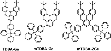 |
| | Scheme 1 Chemical structures of the synthesized TDBA-based host materials. | |
Theoretical calculations and single crystal analysis
To investigate the bonding characteristics between the TDBA moiety and the side group, density functional theory (DFT) and time-dependent DFT (TD-DFT) calculations were performed. Quantum chemical calculations based on DFT were performed using the NWChem program. Theoretical calculations with geometric optimization, single-point energy, HOMO, and LUMO distributions are performed at DFT and TD-DFT levels. The calculations are carried out using the B3LYP functional with def2-TZVPP basis sets, evaluating S1 and T1. Spin–orbit coupling matrix elements were performed using the ORCA program with the same basis set. Fig. 1 and supplementary Fig. S18–S21 (ESI†), along with Tables S1–S4 (ESI†), illustrate the electron density of the HOMO and LUMO orbitals for materials with TPG substitution at para or meta positions of the TDBA moiety.
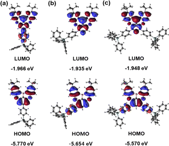 |
| | Fig. 1 Molecular orbitals and energy levels of molecules calculated by DFT theory. (a) TDBA-Ge, (b) mTDBA-Ge and (c) mTDBA-2Ge. | |
The electron density of the HOMO and LUMO for each material is predominantly located on the DOBNA moiety, and the electron density of boron and oxygen within DOBNA is arranged in a manner consistent with conventional DOBNA derivatives. Additionally, in the case of TDBA-Ge with TPG substitution at the para position, the electron density distribution extends to the phenyl group within TPG at the LUMO level, influenced by the electron-withdrawing effect of boron. In contrast, for mTDBA-Ge and mTDBA-2Ge with TPG substitution at the meta position, an extended electron density distribution is observed in the HOMO.14 Introducing substituents at the meta position is expected to result in a redshift of the emission wavelength due to the conjugation extension. The calculated HOMO energy levels for TDBA-Ge, mTDBA-Ge, and mTDBA-2Ge are −5.77, −5.64, and −5.57 eV, respectively, while the LUMO energy levels are −1.97, −1.94, and −1.95 eV, respectively. Consequently, the calculated band gap (ΔEH–L) values show TDBA-Ge (3.80 eV) > mTDBA-Ge (3.72 eV) > mTDBA-2Ge (3.62 eV). The calculated ΔEST values for the newly synthesized host materials, TDBA-Ge, mTDBA-Ge, and mTDBA-2Ge, are 0.515, 0.471, and 0.439 eV, respectively, with a decreasing trend observed from TDBA-Ge to mTDBA-2Ge (Fig. S22, ESI†). Additionally, the spin–orbit coupling (SOC) values at the calculated S1 and T1 states are interpreted. The SOC values for TDBA-Ge, mTDBA-Ge, and mTDBA-2Ge at S1 and T1 are 0.040, 0.102, and 0.114 cm−1, respectively. These values are observed to increase progressively in the order of TDBA-Ge, mTDBA-Ge, and mTDBA-2Ge. This trend in SOC values aligns with the decreasing trend in ΔEST values. Therefore, based on the observed SOC and ΔEST values, mTDBA-2Ge is expected to best fulfill the requirements for MR-TADF among the three structures. Furthermore, upon examining the Tn state energy levels of these host materials, it is noted that T2, T3, and T4 levels are closer to the S1 level than the T1 level. However, in the considered system of this study, a direct RISC process from the T2 level to the S1 level is not anticipated. In this study, the transition from the T1 level to the S1 level is expected to be the primary process.23,24 The optimized structures obtained through molecular calculations reveal dihedral angles between the TDBA moiety and the introduced phenyl groups for TDBA-Ge, mTDBA-Ge, and mTDBA-2Ge as 38.4, 49.0, and 48.1°, respectively (Fig. S23, ESI†). To further investigate these angles, single crystals of the samples were prepared. Single crystals for TDBA-Ge and mTDBA-Ge were grown using the solvent-diffusion crystal growth method with dichloromethane/ethanol (1![[thin space (1/6-em)]](https://www.rsc.org/images/entities/char_2009.gif) :3, v/v). Although the single crystal dihedral angles for TDBA-Ge and mTDBA-Ge were consistent with the calculated values, showing angles of 39 and 44°, respectively (as depicted in Fig. 2), unfortunately, single crystals of mTDBA-2Ge were not obtained. These experimental measurements were found to exhibit values similar to the calculated ones (Fig. S23, ESI†). The molecular packing and intermolecular distances, as well as the plane-to-plane distances, were visualized through single crystal data, presented in Fig. S24 and S25 (ESI†). As seen along the b-axis in Fig. S24 (ESI†), TDBA-Ge showed longer intermolecular distances compared to mTDBA-Ge. Additionally, as depicted in Fig. S25 (ESI†), the intermolecular distances for TDBA-Ge and mTDBA-Ge were determined to be 4.616 and 4.012 Å, respectively. This observation indicated that TDBA-Ge has longer intermolecular distances, suggesting a relatively favorable electro-optical property by inhibiting intermolecular packing.
:3, v/v). Although the single crystal dihedral angles for TDBA-Ge and mTDBA-Ge were consistent with the calculated values, showing angles of 39 and 44°, respectively (as depicted in Fig. 2), unfortunately, single crystals of mTDBA-2Ge were not obtained. These experimental measurements were found to exhibit values similar to the calculated ones (Fig. S23, ESI†). The molecular packing and intermolecular distances, as well as the plane-to-plane distances, were visualized through single crystal data, presented in Fig. S24 and S25 (ESI†). As seen along the b-axis in Fig. S24 (ESI†), TDBA-Ge showed longer intermolecular distances compared to mTDBA-Ge. Additionally, as depicted in Fig. S25 (ESI†), the intermolecular distances for TDBA-Ge and mTDBA-Ge were determined to be 4.616 and 4.012 Å, respectively. This observation indicated that TDBA-Ge has longer intermolecular distances, suggesting a relatively favorable electro-optical property by inhibiting intermolecular packing.
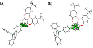 |
| | Fig. 2 Single crystal XRD data for torsions. (a) TDBA-Ge and (b) mTDBA-Ge. | |
Photophysical properties of TDBA-based host materials
To investigate the photophysical characteristics of TDBA-based host materials, ultraviolet-visible (UV-vis) absorption and photoluminescence (PL) spectra were measured in both toluene solution and vacuum-deposited film states (Fig. 3), and a detailed summary of the photophysical properties of TDBA-based host materials is presented in Table 1. In the solution state, TDBA-based host materials exhibited absorption peaks in the range of 389 to 402 nm and confirmed emission in the range of 408 to 432 nm. This corresponds to the absorption wavelength associated with the π–π* transition from the DOBNA backbone.14 In terms of emission, materials mTDBA-Ge and mTDBA-2Ge, with the meta position of TDBA, showed a relatively red-shifted region compared to TDBA-Ge which connected at the para position. This is attributed to the substitution of TPG at the electron lobe position, the meta position of TDBA, resulting in a relatively longer molecular conjugation length than the para position. Furthermore, examining the Stokes shift values, TDBA-Ge, mTDBA-Ge, and mTDBA-2Ge exhibit low Stokes shift values of 19, 27, and 30 nm, respectively, indicating the maintenance of a rigid chemical structure. The FWHM of PL for TDBA-Ge, mTDBA-Ge, and mTDBA-2Ge was found to be 31, 35, and 36 nm, respectively, and the PL quantum yield (PLQY) in the solution state showed values in the range of 50–55%. Analyzing the PL emission data for neat films of TDBA-based host materials reveals PLmax wavelength peaks of 437, 449, and 448 nm for TDBA-Ge, mTDBA-Ge, and mTDBA-2Ge, respectively. mTDBA-Ge and mTDBA-2Ge exhibit a red-shift compared to TDBA-Ge. The FWHM broadened to 76–87 nm for TDBA-Ge, mTDBA-Ge, and mTDBA-2Ge compounds, which is 40–52 nm broader than in the solution state. The FWHM of the DOBNA-OAr film is 57 nm, while the FWHM of the synthesized films for the three materials ranges from 76 to 87 nm.15 The broadened PL spectrum might be interpreted as a phenomenon due to single bond rotation of the TPG within the synthesized structural formula. Even in the previous study with the introduction of TPS, a wide FWHM value of approximately 76 nm was observed, attributed to the free rotation of single bonds enabling various PL transitions. While this phenomenon could be a disadvantage when used as a dopant, it could be advantageous when used as a host. It is because the relatively broad emission spectrum in hosts can increase the possibility of energy transfer to dopants. In the film state, the PLQY for TDBA-Ge, mTDBA-Ge, and mTDBA-2Ge were observed to decrease in the range of 18–25%, compared to the solution state. Experimentally measured HOMO energy levels for TDBA-Ge, mTDBA-Ge, and mTDBA-2Ge were −5.76, −5.62, and −5.76 eV, respectively (Fig. S26, ESI†). The LUMO energy levels were −2.81, −2.68, and −2.91 eV. Consequently, the calculated band gap values followed the order TDBA-Ge (2.95 eV) > mTDBA-Ge (2.94 eV) > mTDBA-2Ge (2.85 eV). The experimentally measured values exhibited a consistent trend with the calculated HOMO and LUMO energy levels, as well as the band gap values. Regarding ΔEST, TDBA-Ge, mTDBA-Ge, and mTDBA-2Ge exhibited values of 0.29, 0.24, and 0.11 eV, respectively, indicating that all three materials possess MR-TADF characteristics. Noteworthy is the lowest value observed for mTDBA-2Ge, suggesting its relatively superior MR-TADF properties (Fig. S27, ESI†). By employing transient PL in the neat films of TDBA-based host materials, delayed fluorescence was observed (Fig. S28 and S29, ESI†). The delayed lifetimes for TDBA-Ge, mTDBA-Ge, and mTDBA-2Ge were 6.98, 6.95, and 6.29 μs, respectively, with mTDBA-2Ge exhibiting a slightly shorter delayed lifetime (Table 1). Based on these values, the calculated rate constant of reverse intersystem crossing (kRISC) in neat films followed the order of TDBA-Ge, mTDBA-Ge, and mTDBA-2Ge, with values of 4.38, 5.98, and 10.17 × 10³ s−1, respectively. With the smallest ΔEST and simultaneously the highest kRISC, mTDBA-2Ge is anticipated to possess excellent MR-TADF characteristics among the synthesized materials, making it promising for achieving high efficiency in devices when applied as a host (Table S5, ESI†).
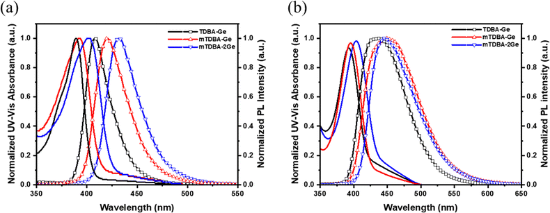 |
| | Fig. 3 UV-vis absorption and photoluminescence analysis of the synthesized materials (a) in the solution state (toluene, 10 × 10−5 M) and (b) in the vacuum-deposited film (thickness: 50 nm). | |
Table 1 Summary of the photophysical properties of the TDBA-based materials
|
|
Solution |
PLQY (%) |
Neat film |
|
λ
ab
(nm) |
λ
em
(nm) |
FWHM (nm) |
λ
ab
(nm) |
λ
em
(nm) |
FWHM (nm) |
PLQY (%) |
E
S/ET/ΔESTb (eV) |
τ
d
(μs) |
HOMOd (eV) |
LUMOd (eV) |
E
g
(eV) |
|
Maximum wavelength in UV-Vis absorption and photoluminescence spectra.
Singlet and triplet energies measured in the neat film state as an onset value (ΔEST = S1 − T1).
Delayed lifetime calculated by PL decay for a vacuum-deposited neat film.
HOMO value measured by UV photoelectron yield spectroscopy (AC-2); the LUMO value was calculated from the optical band gap.
|
|
TDBA-Ge
|
389 |
408 |
31 |
52 |
394 |
437 |
82 |
18 |
3.22/2.93/0.29 |
6.98 |
5.76 |
2.81 |
2.95 |
|
mTDBA-Ge
|
393 |
420 |
35 |
50 |
398 |
449 |
87 |
20 |
3.16/2.92/0.24 |
6.95 |
5.62 |
2.68 |
2.94 |
|
mTDBA-2Ge
|
402 |
432 |
36 |
55 |
406 |
448 |
76 |
25 |
3.05/2.94/0.11 |
6.29 |
5.76 |
2.91 |
2.85 |
Photophysical properties of ν-DABNA-doped films prepared using TDBA-based host materials
The newly synthesized materials were employed as hosts, and films doped with 2 wt% of the blue MR-TADF dopant, ν-DABNA, were analyzed for their photophysical properties. The ν-DABNA dopant, as reported by the Hatakeyama group, has demonstrated high device efficiency characteristics, establishing it as an excellent dopant material.25 By adopting ν-DABNA as a dopant, we investigated the possibility of energy transfer with the TDBA structure containing the TPG moiety (Fig. S30, ESI†). The overlap of the emission spectrum of the host material and the absorption spectrum of the dopant material confirmed the feasibility of Förster energy transfer for all three compounds. Fig. S31 (ESI†) displays the PL spectra for the doped films. All films exhibited a peak maximum at 465 nm, with a bandwidth of 18 nm, displaying PL characteristics similar to those of the previously reported ν-DABNA (Table S6, ESI†). To investigate the excited-state behavior of the doped films with ν-DABNA, transient PL decay was measured (Fig. S32 and S33, ESI†). The tau (τ) values for the doped films using TDBA-Ge, mTDBA-Ge, and mTDBA-2Ge as hosts were 2.73, 3.22, and 2.53 μs, respectively, indicating comparable levels (Table S7, ESI†). The measured PLQY for the doped films revealed values of 29, 24, and 37% for TDBA-Ge, mTDBA-Ge, and mTDBA-2Ge, respectively. Calculating the rate constants to understand the interaction between TDBA-based host materials and ν-DABNA in the doped films (Table S7, ESI†), the kRISC rate constants for TDBA-Ge, mTDBA-Ge, and mTDBA-2Ge were 3.07, 1.78, and 5.52 × 10⁴ s−1, respectively. Similar to the neat films, mTDBA-2Ge exhibited the fastest kRISC rate constant in this aspect as well. This suggests efficient energy transfer in the ν-DABNA-doped system, providing expectations for high efficiency in OLED devices.
Thermal properties
To determine the glass transition temperature (Tg), melting temperature (Tm), and decomposition temperature (Td) of TDBA-based host materials, thermal gravimetric analysis (TGA) and differential scanning calorimetry (DSC) were performed as shown in Fig. S34 and S35 (ESI†). The Td values for 5% weight loss of TDBA-Ge, mTDBA-Ge, and mTDBA-2Ge are 414, 400, and 455 °C, respectively. The Tg/Tm values for TDBA-based host materials are 130/277, 121/183, and 182/385 °C, respectively. Since the Td requirement for OLED materials is at least 300 °C, all three synthesized materials exhibit sufficient thermal stability. Considering that Tg also requires temperatures above 100 °C during OLED operation, the materials satisfy the thermal stability requirements for Tg as well. Low Tg values can induce crystallization of the material morphology during device operation due to Joule heating, leading to efficiency reduction in long-term device operation. Comparing the Tg values of mTDBA-Ge and mTDBA-2Ge, mTDBA-2Ge shows an increase of approximately 60 °C, attributed to the effects of increased symmetry and molecular weight. Additionally, comparing Tg between TDBA-Ge and mTDBA-Ge, TDBA-Ge, which is connected at the para position, shows a Tg increase of 9 °C due to molecular symmetry. This trend in thermal properties remains consistent across Tg, Tm, and Td.
OLED device characterization and performance
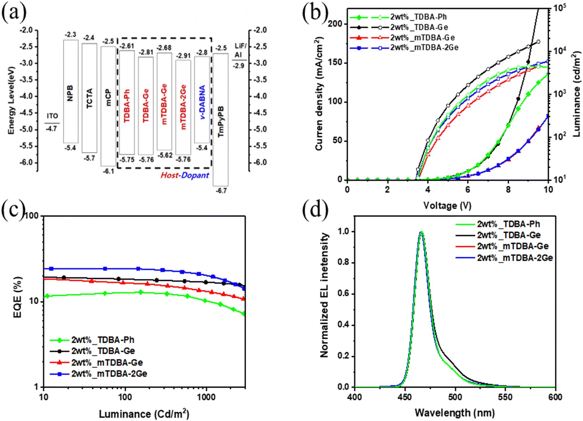
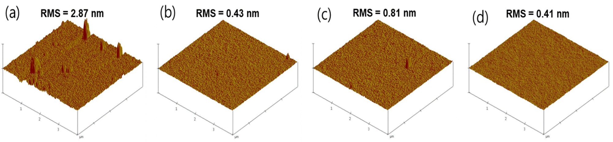
To assess the electroluminescence (EL) performance of the newly synthesized materials, TDBA-Ge, mTDBA-Ge, and mTDBA-2Ge, when used as host materials in the emitting layer, doped OLED devices were fabricated based on a conventional OLED configuration. Typically, structures used as dopants for blue emission exhibit functional groups with a slight electron-donating characteristic, thereby increasing oscillator strength and achieving high EQE. On the other hand, materials used as hosts need to facilitate the simultaneous movement of electrons and holes within the emitter. Therefore, they are structured without groups that push or pull electrons, especially in the case of blue-emitting materials where a wide band gap is essential. The synthesized materials in this study do not contain functional groups with inductive effects and have a wide band gap exceeding 2.85 eV. Therefore, the materials synthesized in this study possess structures more suitable as hosts rather than dopants, and were thus applied as hosts in the device components. The energy level diagram of the fabricated doped OLED devices is depicted in Fig. 4, and the prepared structure is as follows: ITO/NPB (40 nm)/TCTA (15 nm)/mCP (15 nm)/host materials: 2 wt% ν-DABNA (20 nm)/TmPyPB (40 nm)/LiF(1 nm)/Al (200 nm). ITO and Al were used as the anode and cathode. N,N′-Bis(naphthalen-1-yl)-N,N′-bis(phenyl)-benzidine (NPB) and 4,4′,4-tris(carbazol-9-yl)triphenylamine (TCTA) were used as hole injection layers. Additionally, 1,3-bis(carbazol-9-yl)benzene (mCP) served as both the hole transporting layer and the electron blocking layer. 1,3,5-Tris(3-pyridyl-3-phenyl)benzene (TmPyPB) was utilized as the electron transporting layer and stimultaneously as the hole blocking layer. The MR-TADF materials, ν-DABNA, reported by the Hatakeyama group, were employed as a dopant for the emitting layer. Furthermore, the newly synthesized host materials, TDBA-Ge, mTDBA-Ge, and mTDBA-2Ge, were applied to investigate the correlation between the host and dopant materials. For comparison with conventional OLED devices, TDBA-Ph was used as the host material in the reference device (Scheme S2, ESI†). Devices utilizing the three newly synthesized OLED host materials exhibited normal diode characteristics, and based on an EL spectrum with an emission wavelength of 465 nm and a FWHM of 18 nm, they exhibited identical commission internationale de l’eclairage (CIE) coordinates of (0.13, 0.10) (Fig. 4 and Table 2). This consistency aligns with the similarity in FWHM and PL data from the doped films. Under a 1 cd m−2 light intensity condition, all devices showed a low turn-on voltage of 3.0 eV, indicating the use of optimized hole and electron carrier materials, taking into account the energy levels of the emitting layer (EML) (Table 2). When comparing the different devices, the one incorporating the TPG moiety, including a germanium atom, exhibited a relatively higher maximum luminance compared to the device without the TPG moiety, TDBA-Ph. As evident from Fig. 4 and Table 2, the inclusion or exclusion of the TPG moiety demonstrates differences in EL performance. When examining the current efficiency of devices utilizing TDBA-Ge, mTDBA-Ge, and mTDBA-2Ge as hosts at maximum/500 nit/1000 nit, the values are as follows: 17.92/15.28/14.73 cd A−1, 15.12/10.69/9.66 cd A−1, and 19.12/17.05/15.59 cd A−1, respectively. Similarly, the corresponding external quantum efficiency (EQE) values are 19.78/17.52/16.82%, 21.02/14.72/13.23%, and 24.41/22.33/20.43%. When compared to TDBA-Ph, which lacks the TPG moiety and has only a phenyl group substitution, an approximately 1.5–1.8-fold increase in device EQEmax efficiency is observed. Possible explanations for the enhanced EL performance of the TPG-based host materials compared to that of the TDBA-Ph host material are as follows. First, the improved EL performance can be attributed to energy transfer from the TPG-based host materials to the dopant. Larger energy transfer values in the doped TPG-base films were confirmed by the results of Stern–Volmer experiments (Table S8, ESI†). The kq values of the three TPG-based host materials are greater than that of the corresponding TDBA-Ph host material. The calculation of the kFRET values confirmed that the three materials containing the TPG moiety exhibit faster kFRET than the TDBA-Ph host material. These larger energy transfer values could contribute not only to reduced exciton loss but also to increased EL performance. Second, to assess the surface morphology of the TDBA-based host materials, we characterized them using optical microscopy (OM) and atomic force microscopy (AFM) (Fig. S36 (ESI†) and Fig. 5). Films with the TPG moiety, including a germanium atom, exhibited relatively good film uniformity. In contrast, crystallization occurred simultaneously in the TDBA-Ph film. To confirm the improved film surface morphology with the introduction of the TPG group, AFM measurements were conducted on non-doped films fabricated by deposition. In this case, the root mean square (RMS) values for TDBA-Ge, mTDBA-Ge, and mTDBA-2Ge were 0.43, 0.81, and 0.41 nm, respectively, whereas TDBA-Ph exhibited a value of 2.87 nm. The introduction of the TPG group in the three materials resulted in a smoother amorphous thin film morphology compared to TDBA-Ph. Rapid crystallization can lead to decreased device efficiency due to adverse effects such as a rough surface, charge trapping at the interface, and an increase in drift current. The favorable film uniformity of the three synthesized materials may be attributed to the presence of the germanium atom. Third, the improved EL performance of the TPG-containing host materials may be attributed to their excellent thermal stability. TDBA-Ge, mTDBA-Ge, and mTDBA-2Ge exhibit high Tg values in the range of 121–182 °C, whereas TDBA-Ph exhibits a Tg value of 62 °C. Consequently, the TPG-based host materials effectively maintain an amorphous state, because they do not easily undergo molecular changes. The stable surface morphology of the deposited films contributes to maintaining device efficiency. Finally, the long intermolecular distances in host materials based on the bulky TPG group, including a germanium atom, may hinder triplet–triplet annihilation (TTA) and/or singlet–triplet annihilation (STA), leading to an increased EQE. Additionally, the relatively higher EQE of TDBA-Ge compared to mTDBA-Ge can be attributed to the longer intermolecular distances, as explained earlier through single-crystal X-ray diffraction data. This elongation in molecular spacing reduces the likelihood of occurrences where self-quenching factors may arise.
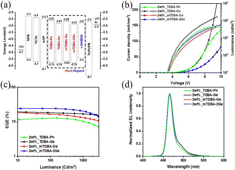 |
| | Fig. 4 OLED device performance of 2 wt%_TDBA-Ge, mTDBA-Ge and mTDBA-2Ge emitters: (a) energy-level diagram of doped OLED devices, (b) current–voltage–luminescence curve, (c) EQE–luminance curves and (d) EL spectra at 10 mA cm−2. | |
Table 2 EL performance of 2 wt% ν-DABNA-doped OLED devices according to the host materials
| EMLs |
T
on
(V) |
L
max (cd m−2) |
CEMaxb |
CE500nitb |
CE1000nitb |
EQEMaxc |
EQE500nitc |
EQE1000nitc |
CIEd (x, y) |
ELmax/FWHM (nm) |
|
Turn-on voltage at 1 cd m−2.
Current efficiency.
External quantum efficiency.
Commission Internationale de l’Eclairage.
|
|
TDBA-Ph:2 wt%_ν-DABNA |
3.1 |
4400 |
10.8 |
9.80 |
8.48 |
12.9 |
11.8 |
10.3 |
(0.13,0.10) |
465/18 |
|
TDBA-Ge:2 wt%_ν-DABNA |
3.0 |
5400 |
17.92 |
15.28 |
14.73 |
19.78 |
17.52 |
16.82 |
(0.13,0.10) |
465/18 |
|
mTDBA-Ge:2 wt%_ν-DABNA |
3.0 |
4500 |
15.12 |
10.69 |
9.66 |
21.02 |
14.72 |
13.23 |
(0.13,0.10) |
465/18 |
|
mTDBA-2Ge:2 wt%_ν-DABNA |
3.0 |
5000 |
19.12 |
17.05 |
15.59 |
24.41 |
22.33 |
20.43 |
(0.13,0.10) |
465/18 |
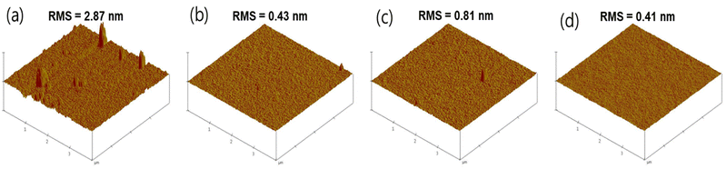 |
| | Fig. 5 AFM images of the non-doped TDBA-based film. (a) TDBA-Ph, (b) TDBA-Ge, (c) mTDBA-Ge, and (d) mTDBA-2Ge. | |
Conclusions
Designing and successfully synthesizing novel host materials for blue MR-TADF, namely TDBA-Ge, mTDBA-Ge, and mTDBA-2Ge, was achieved by introducing the TPG with a germanium atom into the DOBNA moiety, a MR-TADF material. All the three synthesized materials demonstrated high thermal stability, with Tg values exceeding 100 °C. By investigating the EL properties based on the introduced TPG's substitution positions and numbers, OLED device efficiencies for all three materials demonstrated superior EQE compared to TDBA-Ph, where TPG is absent. The introduction of germanium atoms in the TPG facilitated not only energy transfer but also achieved high efficiency through uniform surface characteristics of the thin film and prevention of intermolecular packing. The most optimized structure among the synthesized materials, mTDBA-2Ge, maintained color coordinates of (0.13, 0.10) while exhibiting the highest efficiency, with EQEmax reaching 24.41% among the three materials. Based on these research findings, it is anticipated that various derivatives with bulky side groups containing different heteroatoms can be developed, further advancing the development of high-performance blue MR-TADF hosts.
Author contributions
Conceptualization, S. P. and S. K.; methodology, H. L. and K. L.; validation, H. K., S. P., and K. K.; formal analysis, S. P., S. K. and K. L.; investigation, S. P. and H. K.; resources, T. K. and J. P.; writing – original draft preparation, S. P.; writing – review and editing, H. L. and J. P.; visualization, H. K.; supervision, J. P.; project administration, J. P.; and funding acquisition, J. P.
Conflicts of interest
There are no conflicts to declare.
Acknowledgements
This research was supported by the Basic Science Research Program through the National Research Foundation of Korea (NRF) funded by the Ministry of Education (2020R1A6A1A03048004). This work was partly supported by the GRRC program of Gyeonggi province [(GRRCKYUNGHEE2023-B01), Development of ultra-fine process materials based on the sub-nanometer class for the next-generation semiconductors].
Notes and references
- H. Uoyama, K. Goushi, K. Shizu, H. Nomura and C. Adachi, Nature, 2012, 492, 234–238 CrossRef CAS PubMed.
- K. Goushi, K. Yoshida, K. Sato and C. Adachi, Nat. Photonics, 2012, 6, 253–258 CrossRef CAS.
- J. U. Kim, I. S. Park, C. Y. Chan, M. Tanaka, Y. Tsuchiya, H. Nakanotani and C. Adachi, Nat. Commun., 2020, 11, 1765 CrossRef CAS PubMed.
- Q. Zhang, J. Li, K. Shizu, S. Huang, S. Hirata, H. Miyazaki and C. Adachi, J. Am. Chem. Soc., 2012, 134, 14706–14709 CrossRef CAS PubMed.
- R. Braveenth, H. Lee, J. D. Park, K. J. Yang, S. J. Hwang, K. R. Naveen, R. Lampande and J. H. Kwon, Adv. Funct. Mater., 2021, 31, 2105805 CrossRef CAS.
- S. Wu, W. Li, K. Yoshida, D. Hall, S. Madayanad Suresh, T. Sayner, J. Gong, D. Beljonne, Y. Olivier, I. D. W. Samuel and E. Zysman-Colman, ACS Appl. Mater. Interfaces, 2022, 14, 22341–22352 CrossRef CAS PubMed.
- J. Wang, Y. Yang, F. Gu, X. Zhai, C. Yao, J. Zhang, C. Jiang and X. Xi, ACS Appl. Mater. Interfaces, 2023, 15, 59643–59654 CrossRef CAS PubMed.
- J. M. Teng, Y. F. Wang and C. F. Chen, J. Mater. Chem. C, 2020, 8, 11340 RSC.
- A. Niwa, T. Kobayashi, T. Nagase, K. Goushi, C. Adachi and H. Naito, Appl. Phys. Lett., 2014, 104, 213303 CrossRef.
- S. Oda, B. Kawakami, M. Horiuchi, Y. Yamasaki, R. Kawasumi and T. Hatakeyama, Adv. Sci., 2022, 10, 2205070 CrossRef PubMed.
- J. Wang, J. Zhang, C. Jiang, C. Yao and X. Xi, ACS Appl. Mater. Interfaces, 2021, 13, 57713–57724 CrossRef CAS PubMed.
- J. Wang, Y. Yang, C. Jiang, M. He, C. Yao and J. Zhang, J. Mater. Chem. C, 2022, 10, 3163 RSC.
- T. Hatakeyama, K. Shiren, K. Nakajima, S. Nomura, S. Nakatsuka, K. Kinoshita, J. Ni, Y. Ono and T. Ikuta, Adv. Mater., 2016, 28, 2777 CrossRef CAS PubMed.
- H. Hirai, K. Nakajima, S. Nakatsuka, K. Shiren, J. Ni, S. Nomura, T. Ikuta and T. Hatakeyama, Angew. Chem., Int. Ed., 2015, 54, 13581–13585 CrossRef CAS PubMed.
- Y. Kondo, K. Yoshiura, S. Kitera, H. Nishi, S. Oda, H. Gotoh, Y. Sasada, M. Yanai and T. Hatakeyama, Nat. Photonics, 2019, 13, 678–682 CrossRef CAS.
- Y. Wang, L. Wang, J. Xia, Z. Lai, G. Tian, X. Zhang, Z. Hou, X. Gao, W. Mi, C. Feng, M. Zeng, G. Zhou, G. Yu, G. Wu, Y. Zhou, W. Wang, X. Zhang and J. Liu, Nat. Commun., 2020, 11, 3577 CrossRef PubMed.
- D. H. Ahn, S. W. Kim, H. Lee, I. J. Ko, D. Karthik, J. Y. Lee and J. H. Kwon, Nat. Photonics, 2019, 13, 540–546 CrossRef CAS.
- H. Lim, H. J. Cheon, S. J. Woo, S. K. Kwon, Y. H. Kim and J. J. Kim, Adv. Mater., 2020, 32, 2004083 CrossRef CAS PubMed.
- Y. Kamata, Mater. Today, 2008, 11, 30 CrossRef.
- E. Simoen, J. Mitard, G. Hellings, G. Eneman, B. De Jaeger, L. Witters, B. Vincent, R. Loo, A. Delabie, S. Sioncke, M. Caymax and C. Claeys, Mater. Sci. Semicond. Process., 2012, 15, 588 CrossRef CAS.
- D. P. Brunco, B. De Jaeger, G. Eneman, J. Mitard, G. Hellings, A. Satta, V. Terzieva, L. Souriau, F. E. Leys, G. Pourtois, M. Houssa, G. Winderickx, E. Vrancken, S. Sioncke, K. Opsomer, G. Nicholas, M. Caymax, A. Stesmans, J. Van Steenbergen, P. W. Mertens, M. Meuris and M. M. Heyns, J. Electrochem. Soc., 2008, 155, H552 CrossRef CAS.
-
(a) M.-K. Hung, K.-W. Tsai, S. Sharma, J.-Y. Wu and S.-A. Chen, Angew. Chem., Int. Ed., 2019, 58, 11317–11323 CrossRef CAS PubMed;
(b) M.-K. Hung, K.-W. Tsai, S. Sharma, J. Lei, J.-Y. Wu and S.-A. Chen, ACS Appl. Mater. Interfaces, 2019, 11, 36895–36904 CrossRef CAS PubMed.
- M. K. Etherington, J. Gibson, H. F. Higginbotham, T. J. Penfold and A. P. Monkman, Nat. Commun., 2016, 7, 13680 CrossRef CAS PubMed.
- J. Gibson, A. P. Monkman and T. J. Penfold, ChemPhysChem, 2016, 17, 2956–2961 CrossRef CAS PubMed.
- Y. Kondo, K. Yoshiura, S. Kitera, H. Nishi, S. Oda, H. Gotoh, Y. Sasada, M. Yanai and T. Hatakeyama, Nat. Photonics, 2019, 13, 678–682 CrossRef CAS.
|
| This journal is © The Royal Society of Chemistry 2024 |
Click here to see how this site uses Cookies. View our privacy policy here. 
 Open Access Article
 This Open Access Article is licensed under a Creative Commons Attribution-Non Commercial 3.0 Unported Licence
 a,
Seokwoo
Kang
a,
Ki Ju
Kim
b,
Taekyung
Kim
a,
Seokwoo
Kang
a,
Ki Ju
Kim
b,
Taekyung
Kim